Downloaded 141 times

![[1] Koichi Takeda et al, “A Read Static Noise Margin Free SRAM cell for Low Vdd and High Speed Applications”, Solid-
State Circuits, IEEE Journal vol. 41, Jan.2006, Issue 1 , pp.113-121
[2] M.F. Chang et al., A Differential Data Aware Power-supplied (D2AP) 8T SRAM Cell with Expanded Write / Read
Stabilities for Lower VDDmin Applications. Symposium on VLSI Circuits Digest of Technical Papers, pp. 156–157
(2009a)
[3] M. Yabuuchi et al., A 45 nm 0.6 V Cross-Point 8T SRAM with Negative Biased Read/Write Assist, Symposium on
VLSI Circuits Digest of Technical Papers, pp. 158–159 (2009) 30 2 SRAM Bit Cell Optimization
[4] L. Chang et al., An 8T-SRAM for variability tolerance and low-voltage operation in high performances caches. IEEE
J. Solid-State Circuits, 43, 4, April (2008)
[5] B.H. Calhoun et al., A 256 k Sub threshold SRAM Using 65 nm CMOS. Proceedings of IEEE International Solid-
State Circuits Conference (ISSCC), pp. 628–629, Feb 2006
[6] T.H. Kim et al., A High-Density Sub threshold SRAM with Data–Independent Bitline Leakage and Virtual Ground
Replica Scheme. Proceedings of IEEE International Solid-State Circuits Conference (ISSCC), pp. 330–331, Feb
2007
[7] I.J. Chang et al., A 32 kb 10T sub-threshold SRAM array with bit-interleaving and differential Read scheme in 90
nm CMOS. IEEE J. Solid-State Circuits 44(2), 650–658 (2009b)
[8] J. Wu et al., A Large rVTH/VDD Tolerant Zigzag 8T SRAM with Area-Efficient Decoupled Differential
Technical Papers, pp. 101–102 (2010)
[9] T. Suzuki et al., 0.5 V, 150 MHz, Bulk-CMOS SRAM with Suspended Bit-Line Read Scheme, Proceedings of Sensing
and Fast Write-Back Scheme. Symposium on VLSI Circuits Digest of IEEE European Solid-State Circuits
Conference (ESSCIRC), pp. 354–357, Sept 2010
[10] V. Sharma et al., A 4.4 pJ/Access 80 MHz, 128 kbit variability resilient SRAM with multi-sized sense amplifier
redundancy. IEEE J. Solid-State Circuits, 46, 10 (2011a)
[11] H.Pilo,J.Barwin,G.Braceras,etal.,AnSRAMdesignin65-nmand45-nm technology nodes featuring read and write-
assist circuits to expand operating voltage, Symposiumon VLSI Circuits, Digest of Technical Papers, 2006, pp.15-16.
[12] A. Bhavn agarwala, S. Kosonocky, C. Radens, etal., Fluctuation limits and scaling opportunities for CMOS SRAM
cells, in: Proceedings of International Electron Devices Meeting (IEDM) Technical Digest, 2005, pp.659-662.
17
References
rajeshyadav@itmindia.eduTrade off
Expected
Outcomes References
Thesis Phase - I](https://image.slidesharecdn.com/finalppt-140625065340-phpapp01/75/SRAM-Ultra-low-voltage-operation-17-2048.jpg)
![[13] A. Bhavn agarwala, S. Kosonocky, Y. Chan, etal., Asub-600mV fluctuation tolerant 65nm CMOS SRAM array with
dynamic cell biasing, Symposium on VLSI Circuits Digest of Technical Papers, 2007, pp. 78–79.
[14] M. Yamaoka, N. Maeda, Y. Shinozaki, etal., Low-power embedded SRAM modules with expanded margins
forwriting, IEEE International Solid-State Circuits Conference, Digest of Technical Papers, 2005, pp. 480–611.
[15] K. Zhang, U. Bhattacharya, Z. Chen, etal. A 3-GHz 70-MBSR AM in 65-nm CMOS technology with integrated
column-based dynamic power supply, IEEE J. Solid-State Circuits 41(1)(2006)146–151.
[16] S. Ohbayashi ,M. Yabuuchi, K.Nii ,etal., A 65-nm SoC embedded 6T-SRAM designed for manufactur ability with
read and write operation stabilizing circuits, IEEE J.Solid-State Circuits 42 (4) (2007) 820–829.
[17] K.Sohn,Y.H.Suh,Y.J.Son,etal.,A100-nmdouble-stacked500-MHz72-MB separate I/O synchronous SRAM with
automatic cell-bias scheme and adaptive block redundancy, IEEE International Solid-State Circuits Conference,
Digest of Technical Papers, 2008, pp.386–622.
[18] O .Hirabayashi ,A. Katayama, A. Suzuki, etal., Aprocess-variation-tolerant dual-power-supply SRAM with 0.179-
mm 2 cell in 40-nm CMOS using level-programmable wordline driver, IEEE International Solid-State Circuits
Conference, Digest of Technical Papers, 2009, pp. 458–459.
[19] Y.H.Chen, W.M.Chan, S.Y.Chou, etal., A 0.6-V 45-nm adaptive dual-rail SRAM compiler circuit design for lower
VDDmin VLSIs, Symposiumon VLSI Circuits Digest of Technical Papers, 2008, pp. 210–211.
[20] M. Khellah, N. S. Kim, J. Howard, etal., A 4.2-GHz 0.3-mm 2 256 KB dual-Vcc SRAM building blockin65-
nmCMOS,IEEEInternationalSolid-StateCircuits Conference, DigestofTechnicalPapers,2006,pp.2572–2581.
[21] [13]J.Davis,D.Plass,P.Bunce,etal.,A5.6GHz64-KBdual-readdatacacheforthe POWER6TM
processor,IEEEInternationalSolid-StateCircuitsConference, Digest ofTechnicalPapers,2006,pp.2564–2571.
[22] [14]J.Pille,C.Adams,T.Christensen,etal.,ImplementationoftheCELLbroadband engine ina65-
nmSOItechnologyfeaturingdual-supplySRAMarrays supporting 6GHzat1.3V,IEEEInternationalSolid-
StateCircuitsConference, Digest ofTechnicalPapers,2007,pp.322–606.
[23] [15] M. Yamaoka,K.Osada,K.Ishibashi,0.4-Vlogic–library-friendlySRAMarray using rectangular-
diffusioncellanddelta-boosted-arrayvoltagescheme,IEEE J. Solid-StateCircuits39(6)(2004)934–940.
[24] [16] F.S.Lai,C.F.Lee,On-chipvoltagedownconvertertoimproveSRAMread/write margin andstaticpowerforsub-
nanoCMOStechnology,IEEEJ.Solid-State Circuits 42(9)(2007)2061–2070.
18
References
rajeshyadav@itmindia.eduTrade off
Expected
Outcomes References
Thesis Phase - I](https://image.slidesharecdn.com/finalppt-140625065340-phpapp01/75/SRAM-Ultra-low-voltage-operation-18-2048.jpg)


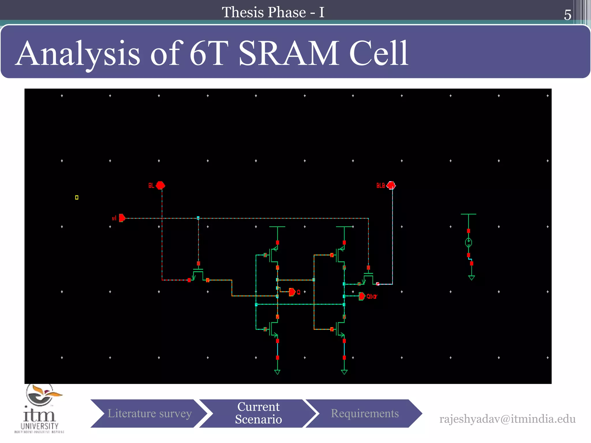
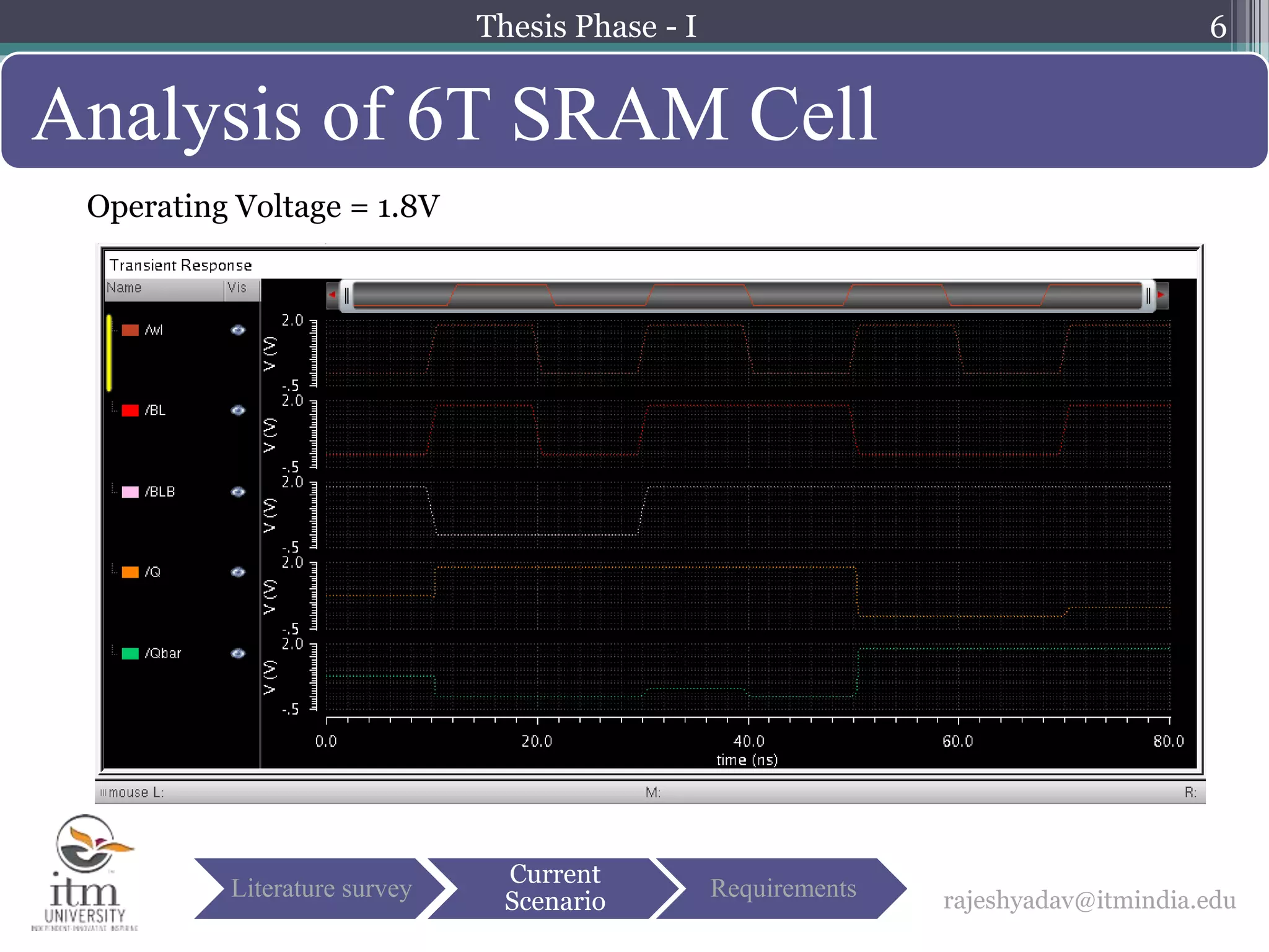
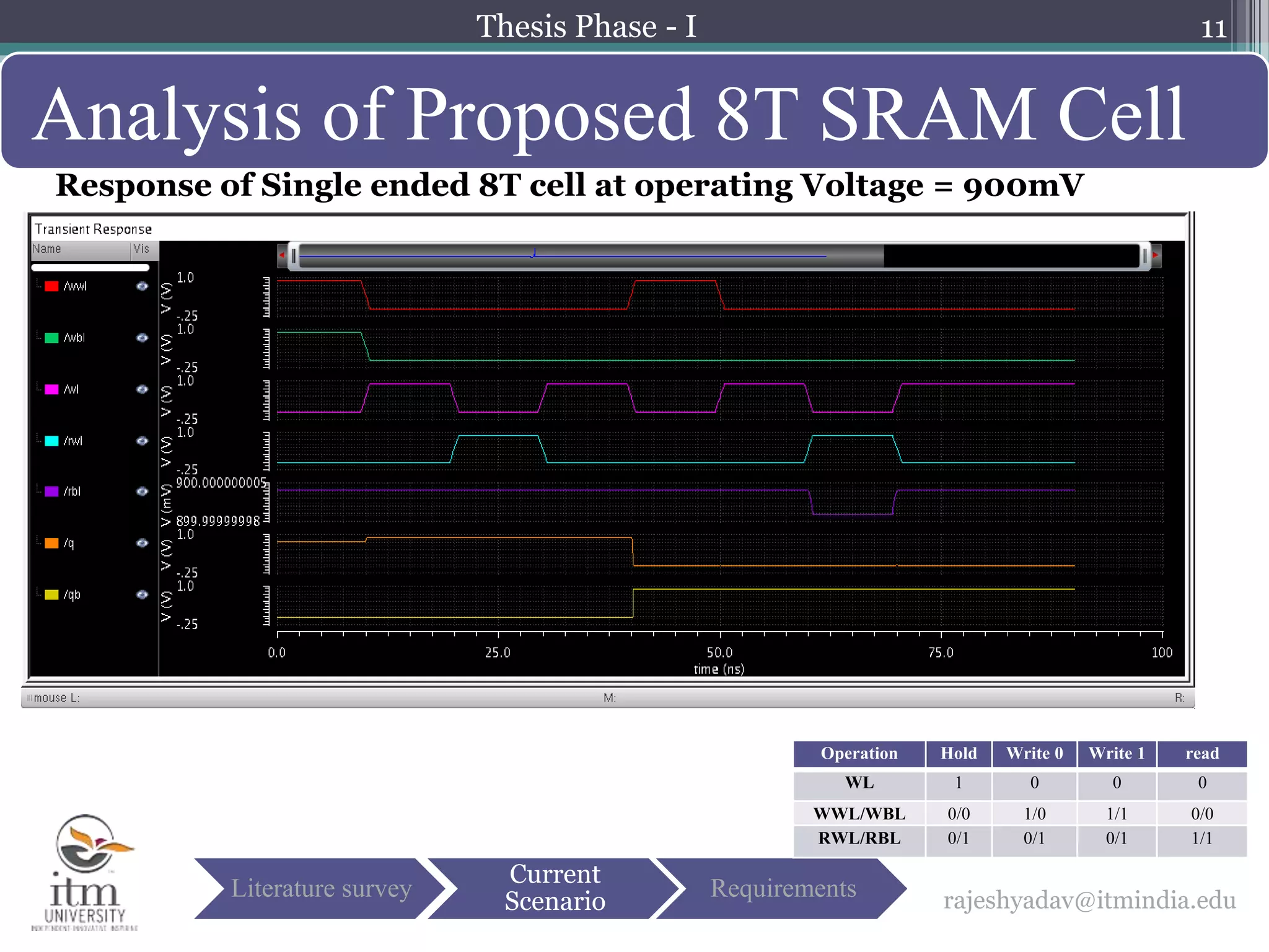
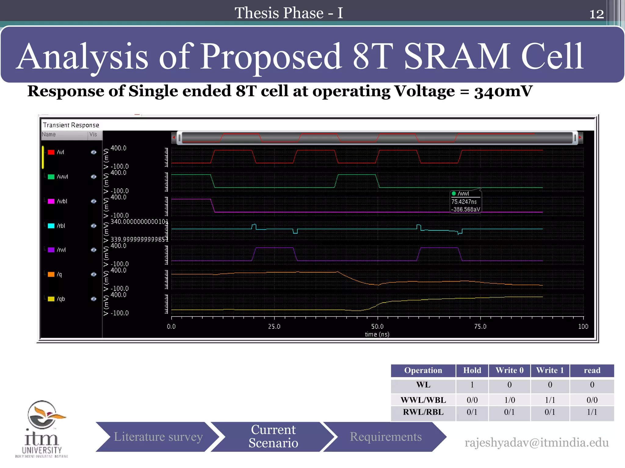
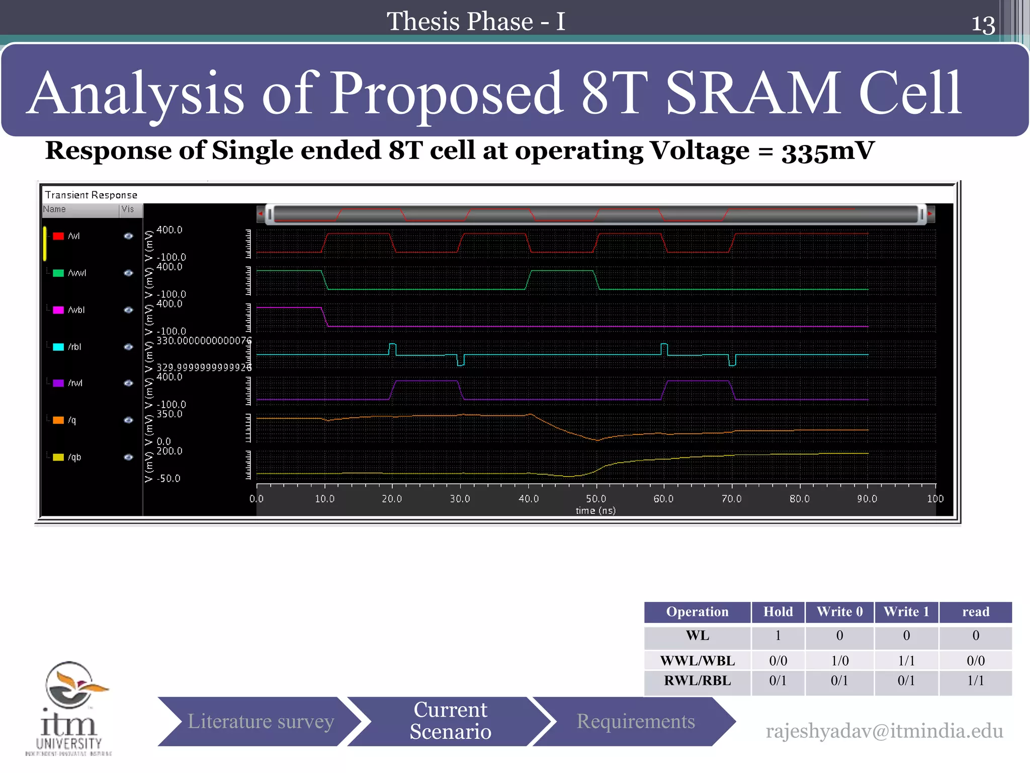
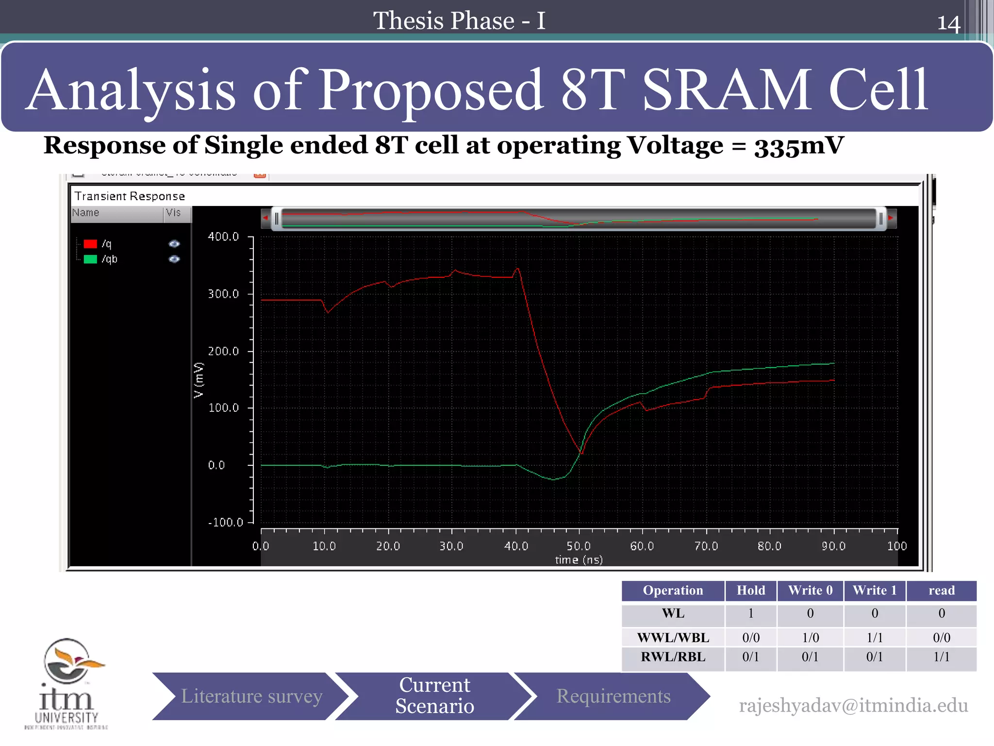
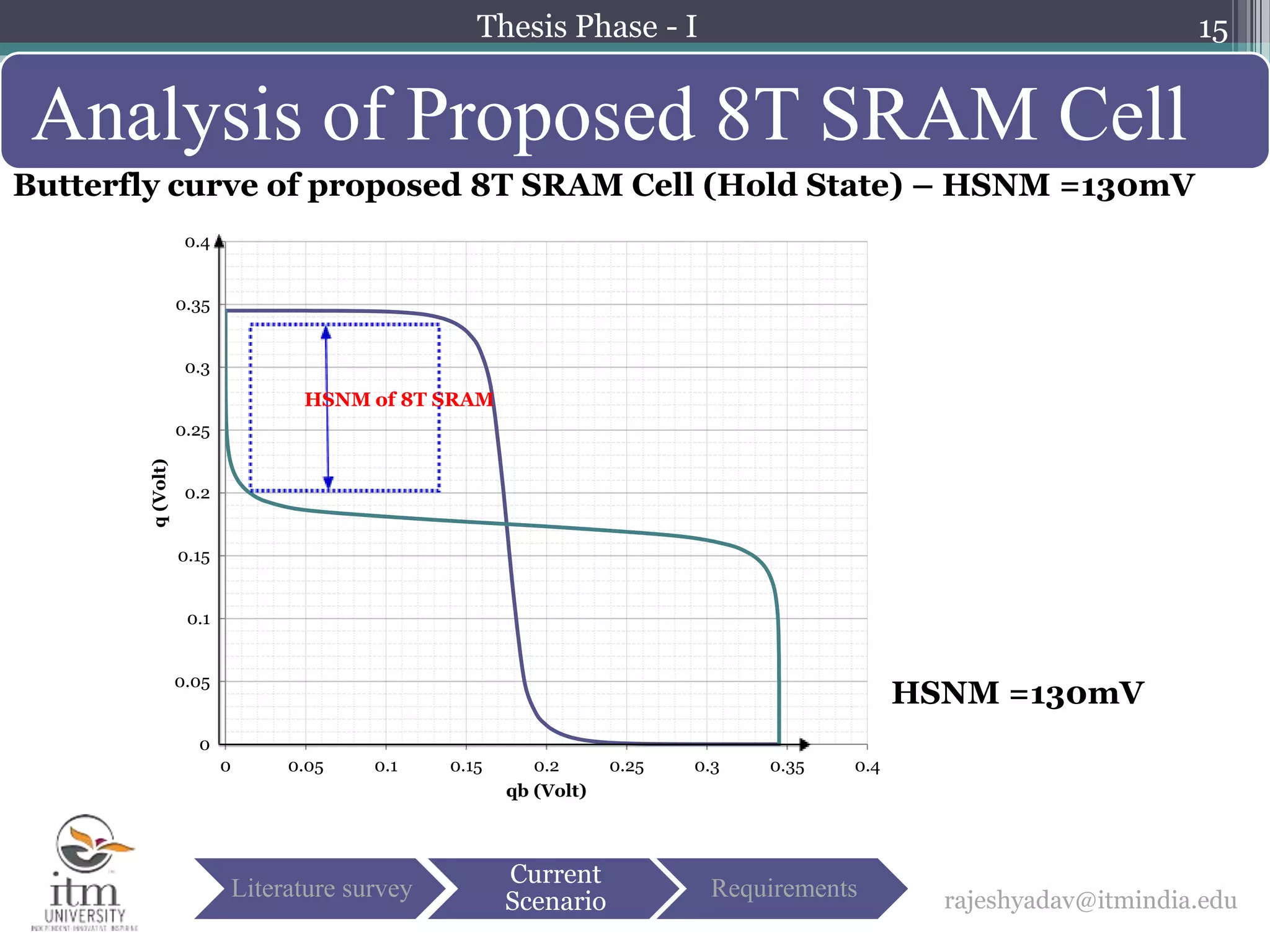
The document describes a proposed novel 8T SRAM cell for ultra-low voltage applications. It begins with an objective to design an 8T SRAM cell that can operate at ultra-low voltages while maintaining low power consumption and improved write and read margins compared to a conventional 6T SRAM cell. It then analyzes the performance of the proposed 8T cell, finding it can operate reliably down to 335mV, with a hold static noise margin of 130mV. The 8T cell exhibits improved write and read stability compared to a 6T cell at ultra-low voltages. In conclusion, the 8T cell design meets the goals of enabling ultra-low voltage operation while improving performance.