Downloaded 16 times
![Aastha Singh et al. Int. Journal of Engineering Research and Applications www.ijera.com
ISSN : 2248-9622, Vol. 5, Issue 4, ( Part -6) April 2015, pp.120-127
www.ijera.com 121 | P a g e
6T. They are compared with respect to power, delay
and speed. Generally, the cell design must strike a
balance between cell area, speed, robustness, leakage
and yield. One of the most important design
objectives is power reduction. However, power
cannot be reduced indefinitely without compromising
the other parameters. As an example, low-power can
compromise the cell area and also the speed of
operations. The mainstream six-transistor (6T)
CMOS SRAM cell is shown in Figure -1, here four
transistors (M1−M4) comprise cross-coupled CMOS
inverters and two NMOS transistors M5 and M6
provide read and write access to the cell. The most
popular SRAM cell is a 6T CMOS SRAM cell due to
its superior robustness, low-voltage and low power
operation [9].
B. Operation of SRAM
The Static Random Access memory device can
perform the operation which is as follows: hold, read
and write.
a. Hold: The access transistors M5 and M6
disconnect the cell from the bit lines, if the word line
is not asserted. The two cross coupled inverters
formed by M1 – M4 will continue to reinforce each
other as long as they are connected to the supply.
b. Read:
Figure 2 Read Operation of SRAM Cell.
The bit lines are pre-charged to VDD prior to
initiating a read operation. The read operation is
initiated by enabling the word line (WL) and
connecting the pre-charged bit lines (BL_1 and
BL_2) to the internal nodes of the cell. On read
access, the bit line voltage VBL_1 remains at the pre-
charge level as shown in Figure-2. The
complementary bit line voltage VBL_2 is discharged
through transistors M1 and M5 connected in series.
Conclusively, transistors M1 and M5 form a voltage
divider whose output is now no longer at zero volts
and is connected to the input of inverter M2−M4 (as
in Figure -1). The sizing of M1 and M5 should ensure
that inverter M2−M4 do not switch causing a
destructive read [9].
c. Write:
Figure 3 Write Operation of SRAM Cell.
While the write operation one of the bit lines i.e.
BL_1 in Figure-3, is driven from pre-charged value
(VDD) to the ground potential by a write driver
through transistor M6. The cell is flipped and its data
is effectively overwritten if transistors M4 and M6
are properly sized. A statistical measure of SRAM
cell write ability is defined as write margin. The write
margin is defined as the minimum bit line voltage
required flipping the state of an SRAM cell. Write
margin value and variation is a function of the
process variation, SRAM array size and cell design.
A cell is considered not writeable if the worst-case
write margin becomes lower than the ground
potential. The write operation is applied to the node
storing a '1'. It is necessitated by the non-destructive
read constraint that ensures that a '0' node does not
exceed the switching threshold of inverter M2−M4.
The only function of pull-up transistors is to maintain
the high level on the '1' storage node and prevent its
discharge by the off state leakage current of the
driver transistor during data retention and to provide
the low-to-high transition during overwriting [13]
2.2 7T SRAM CELL
Figure 4 A 7T SRAM cell](https://image.slidesharecdn.com/s50406120127-150428014815-conversion-gate01/75/A-Comparitive-Analysis-of-Improved-6t-Sram-Cell-With-Different-Sram-Cell-2-2048.jpg)
![Aastha Singh et al. Int. Journal of Engineering Research and Applications www.ijera.com
ISSN : 2248-9622, Vol. 5, Issue 4, ( Part -6) April 2015, pp.120-127
www.ijera.com 122 | P a g e
The circuit of 7T SRAM cell is made of two
CMOS inverters that are connected cross coupled to
each other with additional NMOS Transistor which is
connected to read line and has two pass NMOS
transistors connected to bit lines and bit line bar
respectively. Figure-4 shows circuit of 7T SRAM
cell, where the access transistors M5 is connected to
the word-line (WL) to perform the access write and
M6 is connected to the Read-line (R) to perform the
read operations thought the column bit-lines (BL_1
and BL_2). The bit-lines act as I/O nodes carrying
the data from SRAM cells to a sense amplifier during
read operation or from write in the memory cells
during write operations [12].
2.3 8T SRAM CELL
Figure 5 A 8T SRAM cell
The 8T SRAM circuit [13] is presented in this
section. The schematic of the 8T SRAM cell sized for
an 180nm CMOS technology is shown in Figure 5.
The left sub-circuit of the 8T memory cell is a
conventional 6T SRAM cell with minimum sized
devices (composed of M1, M2, M3, M4, M5, and
M6). Two data access transistors (M5 and M6) and
two bit lines (BL_1 and BL_2) are used for writing to
the SRAM cell. An alternative communication
channel (composed of a separate read bit line RBL
and the transistor stack formed byM7 and M8) is
used for reading the data from the cell.
Two separate control signals RWL and WL are
used for controlling the read and the write operations,
respectively, with the 8T SRAM circuit as shown in
Figure 5. During a read operation, the read signal
RWL transitions to VDD while the write signal WL
is maintained at VGND. The read bit line (RBL) is
conditionally discharged based on the data stored in
the SRAM cell. The storage nodes (Node1 and
Node2) are completely isolated from the bit lines
during a read operation. The data stability is thereby
significantly enhanced as compared to the
conventional 6T SRAM cells [13].
2.4 9T SRAM CELL
Figure 6 A 9T SRAM cell
A 9T SRAM cell is presented in figure-6. The
upper sub-circuit of the new memory cell is
essentially a 6T SRAM cell with minimum sized
devices (composed of M1, M2, M3, M4, M5, and
M6). The two write access transistors (M5 and M6)
are controlled by a write signal (WL). The data is
stored within this upper memory sub-circuit. The
lower sub-circuit of the new cell is composed of the
bit-line access transistors (M7 and M8) and the read
access transistor (M9). The operations of M7 and M8
are controlled by the data stored in the cell. M9 is
controlled by a separate read signal (RD). During a
write operation, WL signal transitions high while RD
is maintained low, as shown in Fig. 2(a). M9 is cut-
off. The two write access transistors M5 and M6 are
turned on. In order to write a “0” to Node1, BL_1 and
BL_2 are discharged and charged, respectively. A
“0” is forced into the SRAM cell through M5.
Alternatively, for writing a “0” to Node2, BL_1 and
BL_2 are charged and discharged, respectively. A
“0” is forced onto Node2 through M6. During a read
operation, RD signal transitions high while WL is
maintained low and the read access transistor M9 is
activated. Provided that Node1 stores “1”. BL is
discharged through M7 and M8. Alternatively,
provided that Node2 stores “1”, the complementary
bit line (BL_2) is discharged through M8 and M9.
Since M5 and M6 are cut-off, the storage nodes
Node1 and Node2 are completely isolated from the
bit lines during a read operation [14].](https://image.slidesharecdn.com/s50406120127-150428014815-conversion-gate01/75/A-Comparitive-Analysis-of-Improved-6t-Sram-Cell-With-Different-Sram-Cell-3-2048.jpg)
![Aastha Singh et al. Int. Journal of Engineering Research and Applications www.ijera.com
ISSN : 2248-9622, Vol. 5, Issue 4, ( Part -6) April 2015, pp.120-127
www.ijera.com 123 | P a g e
III. IMPROVED 6T SRAM CELL
Figure 7 Improved 6T SRAM cell
The improved 6T SRAM cell is shown in Figure 7, it
consists of two additional PMOS and NMOS
transistor in which NMOS transistor is connected to
the pull down network of SRAM cell and other is
connected to the Pull up network of the SRAM cell.
The input of the gate of NMOS transistor of pull
down network of the SRAM cell is connected Vdd
and the input gate of PMOS transistor of pull up
network of the SRAM cell is connected to ground.
This whole modification in the circuit of the SRAM
offers the lower power consumption, less delay and
high SNM. This improved 6T SRAM cell shows
maximum reduction in power consumption of 88%,
maximum reduction in delay of 64% and maximum
SNM of 17% increases compared with 7T SRAM
cell. However, the read and write operations of given
circuit is same as that of conventional 6T CMOS
SRAM cell.
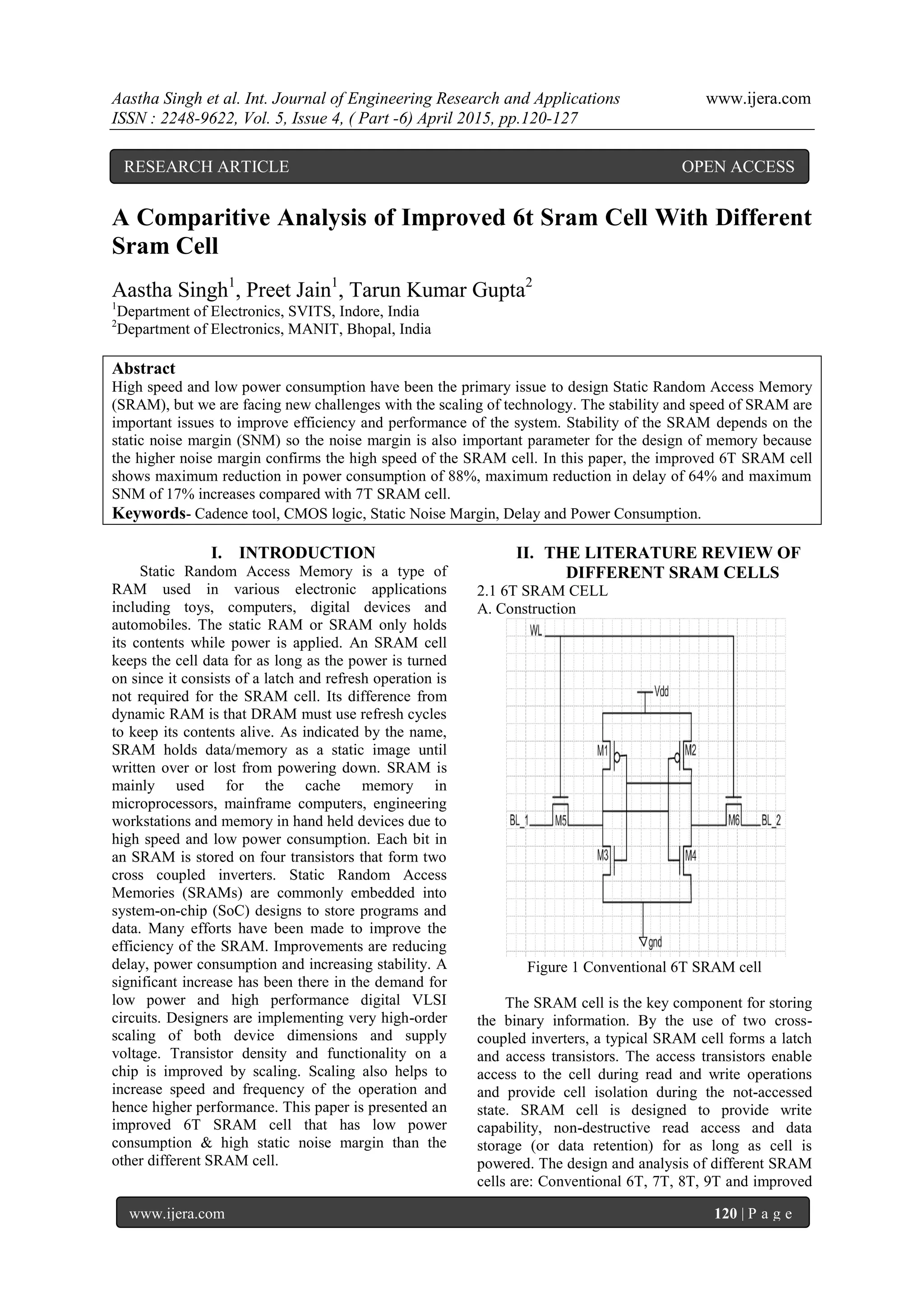
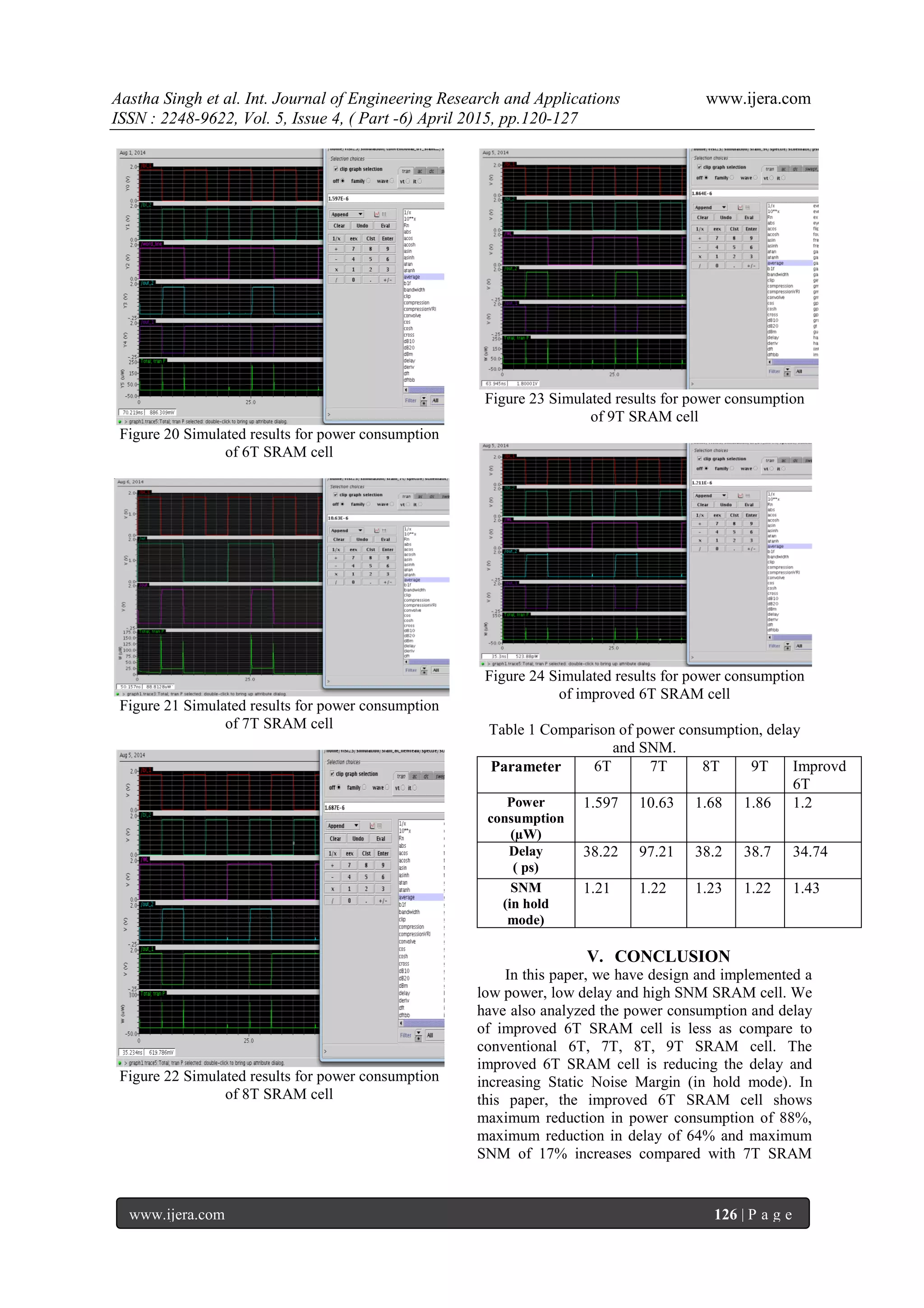
IV. SIMULATION AND RESULTS
The Simulation and result of the improved 6T
SRAM cell is presented in Table 1. In the following
subsections, three important metrics of an SRAM
design: Static noise margins, power, and delays are
explaining.
4.1 STATIC-NOISE-MARGIN (SNM)
The stability of SRAM circuit depends on the
Static Noise Margin. The basic SNM is obtained by
drawing and mirroring the inverter characteristics and
finding the maximum possible square between them.
It is a graphical technique of estimating the SNM.
Figure 8 The standard setup for SNM definition
Figure 9 General SNM characteristics during
Hold operation
The Figure-9 shows a common way of
representing the SNM graphically for a bit-cell
holding data. This figure plots the Voltage Transfer
Characteristic (VTC) of Inverter 2 (inv2) and the
inverse VTC-1 from Inverter 1(inv1). Resulting two-
lobed curve is called a 'butterfly curve' and is used to
determine the SNM. The length of the side of the
largest square that can be embedded inside the lobes
of the butterfly curve is defined as the SNM.
Consider the case when the value of the noise sources
with value Vn are introduced in the bit cell at each of
the internal nodes. When the value of Vn increases
from 0, it causes the VTC-1 for first inverter in
Figure-9 to move downward and the VTC for the
second inverter to move to the right. The values of
SNM vary in different operation modes. SNM is
becoming important factor to check the stability
during read operation. SRAM cell immunity to static
noise is measured in terms of SNM that quantifies the
maximum amount of voltage noise that can be
tolerated at the cross-inverters output nodes without
flipping the cell. The value of the SNM during cell
operation changes with any change in the noise.
Although the SNM is important during hold, the cell
stability during active operation represents a more
significant limitation to SRAM operation [8].](https://image.slidesharecdn.com/s50406120127-150428014815-conversion-gate01/75/A-Comparitive-Analysis-of-Improved-6t-Sram-Cell-With-Different-Sram-Cell-4-2048.jpg)
![Aastha Singh et al. Int. Journal of Engineering Research and Applications www.ijera.com
ISSN : 2248-9622, Vol. 5, Issue 4, ( Part -6) April 2015, pp.120-127
www.ijera.com 124 | P a g e
Figure 10 Butterfly curve for SNM of 6T SRAM cell
Figure11 Butterfly curve for SNM of 7T SRAM cell
Figure 12 Butterfly curve for SNM of 8T SRAM cell
Figure 13 Butterfly curve for SNM of 9T SRAM cell
Figure 14 Butterfly curve for SNM of Improved 6T
SRAM cell
4.2- DELAY
The delays of SRAM are usually defined as the
time it takes to read or write a value from an SRAM
cell. While a node is switching, the delay is measured
as the time difference between 10% and 90% of the
voltage swing. As an example - if we are trying to
bring node A from 0V to 1V then the delay is the
time it takes for node A to go from 0.1V to 0.9V. In
case of a write operation, write delay is defined as the
time required for writing '0'to storage node 'L' from
the time when word Line is activated to the time
when 'L' falls to 10% of its initial high level. In the
same way, writing '1' to 'L' is defined from the time
when word Line is activated to the time when 'L' rises
to 90% of its full swing from its initial low level.
Write delay is approximately equal to the propagation
delay of inv2 and inv l [2].](https://image.slidesharecdn.com/s50406120127-150428014815-conversion-gate01/75/A-Comparitive-Analysis-of-Improved-6t-Sram-Cell-With-Different-Sram-Cell-5-2048.jpg)
![Aastha Singh et al. Int. Journal of Engineering Research and Applications www.ijera.com
ISSN : 2248-9622, Vol. 5, Issue 4, ( Part -6) April 2015, pp.120-127
www.ijera.com 125 | P a g e
Figure 15 Simulated results for delay of 6T SRAM
cell
Figure 16 Simulation results for delay of 7T SRAM
cell
Figure 17 Simulation results for delay of 8T SRAM
cell
Figure 18 Simulated results for delay of 9T SRAM
cell
Figure 19 Simulation results for delay of improved
6T SRAM cell
4.3- POWER CONSUMPTION
The power consumption of Static Random
Access Memory cell depends on consumption of the
power which used to perform the operation of the
transistor [5]. Dynamic power consumption in
SRAMs is consumed due to the charging and
discharging capacitances during read and write
operation and during each cycle of SRAM particular
amount of Energy is drawn from the power supply
and dissipated. For each cycle the power
consumption is depended on the type of operation
(read or write). Also, when the capacitor charged
from GND to VDD and then discharged VDD to
GND, the amount of energy drawn from the power
supply and dissipated equals CLVDD
2
. The stored
energy on the capacitor CL with voltage VC equals ½
CLVC
2
. Therefore, each time the capacitor CL is
charged from VC to VDD and then discharged VDD to
VC [3]. A average power dissipation of any device
over one period can be obtained by following
expression [6].
Pav = [(1/T) 0∫T
I dt] × V](https://image.slidesharecdn.com/s50406120127-150428014815-conversion-gate01/75/A-Comparitive-Analysis-of-Improved-6t-Sram-Cell-With-Different-Sram-Cell-6-2048.jpg)
![Aastha Singh et al. Int. Journal of Engineering Research and Applications www.ijera.com
ISSN : 2248-9622, Vol. 5, Issue 4, ( Part -6) April 2015, pp.120-127
www.ijera.com 127 | P a g e
cell. Therefore, improved 6T SRAM cell is useful for
high-speed and low power applications.
REFERENCE
[1] Ajoy C A, Arun Kumar, Anjo C A, Vignesh
Raja: “Design and Analysis of Low Power
Static RAM Using Cadence Tool in 180nm
Technology”, IJCST Vol. 5, SPL - 1, Jan -
March 2014.
[2] A. Islam and M. Hasan, Member: “Leakage
Characterization of 10T SRAM Cell”, IEEE
Transaction on Electron Device, Vol. 59,
March 2012.
[3] Sushil Bhushan, Shishir Rastogi, Mayank
Shastri: “High Density Four-Transistor
SRAM cell with low power consumption”,
IJCTA, Spt-Oct 2011.
[4] L. Chang: “An 8T-SRAM for Variability
Tolerance and Low-Voltage Operation in
High-Performance Caches”, IEEE Journal
of Solid-State Circuits, Vol. 43, April 2008.
[5] Shyam AKASHE, Sushil BHUSHAN,
Sanjay SHARMA: “High Density and Low
Leakage Current Based 5T SRAM Cell
Using 45 nm Technology”, Roman Journal
of Information Science and Technology
Volume 15, Number 2012.
[6] Kang S.-M., Leblebici Y., CMOS Digital
Integrated Circuits-Analysis and Design,
third edition, WCB McGraw-Hill, 2003.
[7] Ramy E. Aly, Md I. Faisal and Magdy A.
Bayoumi: “Novel 7T SRAM cell for low
power cache design”, 0-7803-9264-
71051$20.002005 IEEE.
[8] Nahid Rahman, B. P. Singh: “Design of Low
Power Sram Memory Using 8t Sram Cell”,
International Journal of Recent Technology
and Engineering, Volume-2, Issue-1, March
2013.
[9] Sunil Kumar Ojha & P.R. Vaya: “A Novel
Architecture of SRAM Cell for Low-Power
Application”, ISSN (Print): 2278-8948,
Volume-2, Issue-4, 2013.
[10] Michael C. Wang: “Low Power Dual Word
Line 6-Transistor”, Proceedings of the
World Congress on Engineering and
Computer Science 2009 Vol 1 WCECS
2009, October 2009.
[11] K. Dhanumjaya, Dr. MN. Giri Prasad, Dr.
K. Padmaraju , Dr. M. Raja Reddy: “Design
of Low Power SRAM in 45 nm CMOS
Technology”, International Journal of
Engineering Research and Applications
(IJERA), Vol. 1, Issue 4, pp.2040-2045.
[12] Pankaj Agarwal, Nikhil Saxena: “Low
Power Design and Simulation of 7T SRAM
Cell using various Circuit Techniques”
International Journal of Engineering Trends
and Technology (IJETT), Vol. 4, May 2013.
[13] Sherif A.Tawfik and Volkan Kursun:
“Stability Enhancement Techniques for
Nanoscale SRAM Circuits: A Comparison”,
International SoC Design Conference, 2008.
[14] Zhiyu Liu and Volkan Kursun:
“Characterization of a Novel Nine-
Transistor SRAM Cell” IEEE Transaction on
Very Large Scale Integration (VLSI)
System, Vol. 16, April 2008.](https://image.slidesharecdn.com/s50406120127-150428014815-conversion-gate01/75/A-Comparitive-Analysis-of-Improved-6t-Sram-Cell-With-Different-Sram-Cell-8-2048.jpg)

The document presents a comparative analysis of improved 6T SRAM cells with other SRAM designs, highlighting advancements in speed, power consumption, and static noise margin. The improved 6T SRAM cell achieves an 88% reduction in power consumption and a 64% reduction in delay compared to 7T cells. The study emphasizes the importance of stability and performance in the design of static random access memory for digital VLSI applications.


