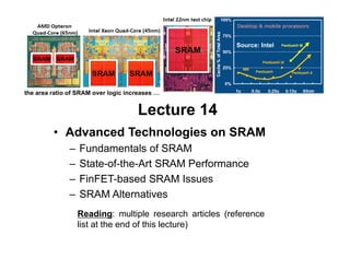
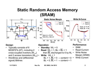
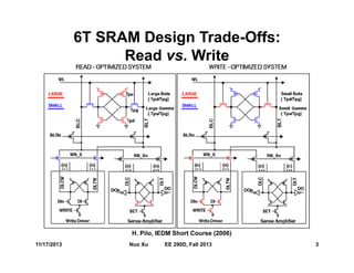
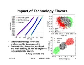
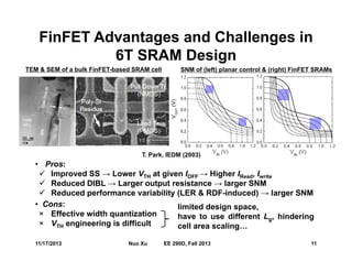
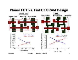
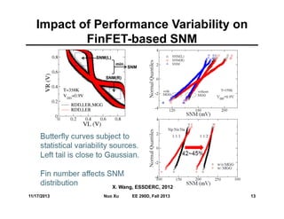
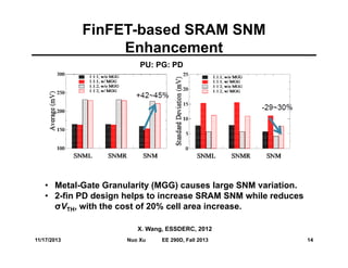
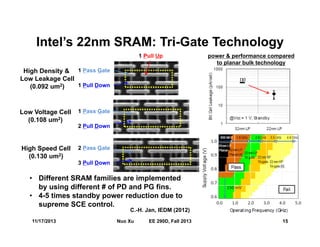
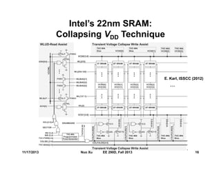
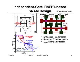
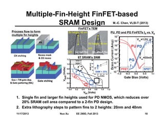
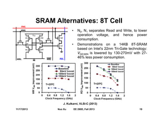
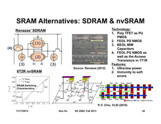
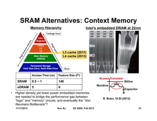
Lecture 14
• Advanced Technologies on SRAM
– Fundamentals of SRAM
– State-of-the-Art SRAM Performance
– FinFET-based SRAM Issues
– SRAM Alternatives
the area ratio of SRAM over logic increases …
Reading: multiple research articles (reference
list at the end of this lecture)
Source: Intel
Static Random Access Memory
(SRAM)
11/17/2013 2Nuo Xu EE 290D, Fall 2013
Design:
• Typically consists of 6
MOSFETs (6T), including 2
cross-coupled invertors (M1-4)
and 2 access transistors (M5,6)
• Wordlines and (differential
signal) Bitlines
Operation:
• Standby: WL = 0
• Read: WL = 1, BL = BL = 1
then BL discharged to 0 by M1
• Write: WL = 1
BL = 1, BL = 0 → content = 0
BL = 0, BL = 1 → content = 1
Pass Gate
Pull Down
Pull Up
Pass Gate
Tech. A
Tech. B
Tech. A
Tech. B
Tech. A
Tech. B
Tech. A
Tech. B
Static Noise Margin Write N-Curve
VR (V)
VL(V)
Performance:
• SNM
• Read Current
• Write Noise
Margin (WNM)
• Write Current
6T SRAM Design Trade-Offs:
Read vs. Write
11/17/2013 3Nuo Xu EE 290D, Fall 2013
H. Pilo, IEDM Short Course (2006)
SRAM Technology Scaling Challenges
11/17/2013 4Nuo Xu EE 290D, Fall 2013
Alpha-ray
Nuclear reaction
Cosmic-ray neutron
Soft-Errors
Gate LeakageReduced VDDDegraded Electrostatics
Variability
Impacts of Performance Variability
• Immunity to short-channel effects, as well as performance
variations is needed to achieve high SRAM cell yield.
• SRAM always uses minimum transistor size, to reduce cell area.
→ Poor immunity to random and systematic variability
• Read vs. Write conflicts; Voltage loss on PG during Read
• VTH mismatch results in significantly reduced SNM.
→ Lowers SRAM cell yield, and limits VDD scaling
11/17/2013 5Nuo Xu EE 290D, Fall 2013
- Why variability is extremely harmful to SRAM?
J. Luo, SSDM (2010) K. Zhang, VLSI (2004)
0.05 0.1 0.15 0.2 0.25 0.3 0.35
0.001
0.003
0.01
0.02
0.05
0.10
0.25
0.50
0.75
0.90
0.95
0.98
0.99
0.997
0.999
VT (V)
Probability
Fast Corner: DATA
Nominal : DATA
Slow Corner: DATA
BSIM CMG
Impact of Technology Flavors
11/17/2013 6Nuo Xu EE 290D, Fall 2013
• Different technology favors are
implemented by VTH engineering
• Fast switching device has less Read
and Write stability, as well as larger cell
leakage (standby power).
X. Wang, ESSDERC, 2012
Circuit Techniques to Improve SRAM
Stability
11/17/2013 7Nuo Xu EE 290D, Fall 2013
Dynamic VDD Floating VDD
Negative BL
K. Zhang,
ISSCC (2005)
M. Yamaoka,
ISSCC (2004)
H. Pilo,
ISSCC (2011)
M.E. Sinangil,
ISSCC (2011)
Pulsing WL
45nm 6T SRAM Design Rules
11/17/2013 8Nuo Xu EE 290D, Fall 2013
Cell Size : 0.72×0.345=0.248um2
PD NMOS: W/Lg = 85/34 nm
PG NMOS: W/Lg = 65/39 nm
PU PMOS: W/Lg = 65/34 nm
Contact Size : 66nm
Gate-Cont. space : 35nm
Well Isolation : 100nm
P+/P+ Isolation: 70nm
DT Ratio : 1.50
DT Ratio(W) : 1.31
• Imposed by OPC, SRAM cell layout evolved from arbitrary shapes to
predominantly straight lines and holes.
• Imposed by Double Patterning, poly-gates are oriented in the same direction
H. Nii, IEDM (2006) & after S. Yu (ASU, 2013)
State-of-the-Art SRAM Cell Area
0.1 um2
Intel 22nm Tri-Gate IBM 22nm FinFET TSMC 20nm FinFET
0.094 um2
0.076 um2
0.063 um2
IBM 22nm PD-SOI
0.1 um2
Planar Platforms
Samsung 20nm Bulk
911/17/2013
State-of-the-Art SRAM Performance
Company Node
(nm)
Area
(um2)
VDD,1
(V)
SNM1
(V)
VDD,2
(V)
SNM2
(V)
Ref.s
Intel 32 0.171 ~0.9 ~0.2 IEDM 09
TSMC 32 0.15 1.0 0.22 0.8 0.2
IBM 32 0.157 0.9 0.213 IEDM 08
UMC 28 0.124 0.9 0.179 0.7 0.144 VLSI 11
Samsung 20 0.9 0.255 IEDM 11
IBM 22
PDSOI
0.1 0.9 0.22 0.7 0.148 IEDM 08
IBM 22 0.094
0.063
0.8
0.8
0.2
0.15
0.4
0.4
0.1
0.05
VLSI 10
TSMC 20 0.1 0.85
0.65
0.45 0.09 IEDM 10
Intel 22 0.092
0.108
ISSCC 12
PlanarBulkMOSFETFinFETs
11/17/2013 10Nuo Xu EE 290D, Fall 2013
FinFET Advantages and Challenges in
6T SRAM Design
11/17/2013 11Nuo Xu EE 290D, Fall 2013
TEM & SEM of a bulk FinFET-based SRAM cell SNM of (left) planar control & (right) FinFET SRAMs
• Pros:
 Improved SS → Lower VTH at given IOFF → Higher IRead, Iwrite
 Reduced DIBL → Larger output resistance → larger SNM
 Reduced performance variability (LER & RDF-induced) → larger SNM
• Cons:
× Effective width quantization
× VTH engineering is difficult
limited design space,
have to use different Lg, hindering
cell area scaling…
T. Park, IEDM (2003)
Planar FET vs. FinFET SRAM Design
PassGate Pull-Up Pull-Down
PassGate Pull-UpPull-Down
11/17/2013 12Nuo Xu EE 290D, Fall 2013
Planar FET FinFET
Impact of Performance Variability on
FinFET-based SNM
11/17/2013 13Nuo Xu EE 290D, Fall 2013
X. Wang, ESSDERC, 2012
SNM(L)
SNM(R)
SNM
min
11/17/2013 14Nuo Xu EE 290D, Fall 2013
FinFET-based SRAM SNM
Enhancement
PU: PG: PD
• Metal-Gate Granularity (MGG) causes large SNM variation.
• 2-fin PD design helps to increase SRAM SNM while reduces
σVTH, with the cost of 20% cell area increase.
X. Wang, ESSDERC, 2012
Intel’s 22nm SRAM: Tri-Gate Technology
11/17/2013 15Nuo Xu EE 290D, Fall 2013
C.-H. Jan, IEDM (2012)
1 Pull Up
1 Pull Down
1 Pass Gate
2 Pull Down
1 Pass Gate
3 Pull Down
2 Pass Gate
High Density &
Low Leakage Cell
(0.092 um2)
Low Voltage Cell
(0.108 um2)
High Speed Cell
(0.130 um2)
power & performance compared
to planar bulk technology
• Different SRAM families are implemented
by using different # of PD and PG fins.
• 4-5 times standby power reduction due to
supreme SCE control.
Intel’s 22nm SRAM:
Collapsing VDD Technique
11/17/2013 16Nuo Xu EE 290D, Fall 2013
E. Karl, ISSCC (2012)
Independent-Gate FinFET-based
SRAM Design Z. Guo, ISLPED (2005)
11/17/2013 17Nuo Xu EE 290D, Fall 2013
• Enhanced Read margin
• Reduced WL capacitance
• IREAD nearly unaffected
Multiple-Fin-Height FinFET-based
SRAM Design M.-C. Chen, VLSI-T (2013)
11/17/2013 18Nuo Xu EE 290D, Fall 2013
Process flow to form
multiple fin heights
FinFET’s TEM
PU, PD and PG FinFETs Id vs. Vg
1. Single fin and larger fin heights used for PD NMOS, which reduces over
20% SRAM cell area compared to a 2-fin PD design.
2. Extra lithography steps to pattern fins to 2 heights: 20nm and 40nm
6T SRAM’s SNM
SRAM Alternatives: 8T Cell
11/17/2013 19Nuo Xu EE 290D, Fall 2013
J. Kulkarni, VLSI-C (2013)
• N0, N1 separates Read and Write, to lower
operation voltage, and hence power
consumption.
• Demonstrations on a 14KB 8T-SRAM
based on Intel’s 22nm Tri-Gate technology:
VDD,MIN is lowered by 130-270mV with 27-
46% less power consumption.
SRAM Alternatives: SDRAM & nvSRAM
11/17/2013 20Nuo Xu EE 290D, Fall 2013
Renasas’ SDRAM
8T2R nvSRAM
P.-F. Chiu, VLSI (2010)
RRAM Switching
Characteristics
Technology:
1. Poly TFET as PU
PMOS
2. FEOL PD NMOS
3. BEOL MIM
Capacitors
4. FEOL PG NMOS as
well as the Access
Transistors in 1T1R
Features:
1. Ultra-low power
2. Immunity to soft
errors
Source: Renasas (2012)
(4)
SRAM Alternatives: Context Memory
11/17/2013 21Nuo Xu EE 290D, Fall 2013
Bitline
Wordline
Capacitor
Access Transistor
M2
M3
M4
Memory Hierarchy Intel’s embedded DRAM at 22nm
R. Brain, VLSI (2013)
L3 cache (2011)
L4 cache (2013)
• Higher density yet lower power embedded memories
are needed to bridge the performance gap between
“logic” and “memory” circuits, and eventually the “Von
Neumann Bottleneck”?
Access Time (ns) Feature Size (F2)
SRAM 0.5 ~ 1 146
eDRAM 5 6
References
SRAM Technology
1. X. Wang et al., “Statistical Variability in 14nm Node SOI FinFETs and its Impact on Corresponding
6T-SRAM Cell Design,” ESSDERC, pp. 113-116, 2012.
2. (IBM 32nm) F. Arnaud et al., “32nm General Purpose Bulk CMOS Technology for High
Performance Applications at Low Voltage,” IEEE International Electron Device Meeting Tech. Dig.,
pp.633-636, 2008.
3. (UMC 28nm) C.W. Liang et al., “A 28nm Poly/SiON CMOS Technology for Low Power SoC
Applications,” Symposium on VLSI Technology Dig., pp.38-39, 2011.
4. (IBM 22nm PDSOI) B.S. Haran et al., “22nm Technology Compatible Fully Functional 0.1um2 6T-
SRAM Cell,” IEEE International Electron Device Meeting Tech. Dig., 2008.
5. (Samsung 20nm) H.-J. Cho et al., “Bulk Planar 20nm High-K/Metal Gate CMOS Technology
Platform for Low Power and High Performance Applications,” IEEE International Electron Device
Meeting Tech. Dig., pp.350-353, 2011.
6. (Samsung Bulk FinFET) T. Park et al., “Static Noise Margin of the Full DG CMOS SRAM Cell
Using Bulk FinFETs (Omega MOSFETs),” IEEE International Electron Device Meeting Tech. Dig.,
2003.
7. (IBM SOI FinFET) V.S. Basker et al., “A 0.063um2 FinFET SRAM Cell Demonstration with
Conventional Lithography using a Novel Integration Scheme with Aggressively Scaled Fin and
Gate Pitch,” Symposium on VLSI Technology Dig., pp.19-20, 2010.
8. (TSMC Bulk FinFET) C.C. Wu et al., “High Performance 22/20nm FinFET CMOS Devices with
Advanced High-/Metal Gate Scheme,” IEEE International Electron Device Meeting Tech. Dig.,
pp.600-603, 2010.
9. (nvSRAM) P.-F. Chiu et al., “A Low Store Energy, Low VDDmin, Nonvolatile 8T2R SRAM with 3D
Stacked RRAM Devices for Low Power Mobile Applications,” Symposium on VLSI Technology
Dig., pp.229-230, 2010.
References
SRAM Circuits
10. M. Yamaoka et al., “A 300 MHz 25uA/Mb Leakage On-Chip SRAM Module Featuring Process-
Variation Immunity and Low-Leakage-Active Mode for Mobile-Phone Application Processors,”
ISSCC, pp.494-495, 2004.
11. K. Zhang et al., “A 3GHz 70Mb SRAM in 65nm CMOS Technology with Integrated Column based
Dynamic Power Supply,” ISSCC, pp.474-476, 2005.
12. M.E. Sinangil et al., “A 28 nm High-Density 6T SRAM with Optimized Peripheral Assist Circuits for
Operation Down to 0.6V,” ISSCC, pp.260-262, 2011.
13. H. Pilo et al., “A 64Mb SRAM in 32nm High-k Metal-Gate SOI Technology with 0.7V Operation
Enabled by Stability, Write-Ability and Read-Ability Enhancements,” ISSCC, pp.254-256, 2011.
Intel’s Tri-Gate Platform
14. E. Karl et al., “A 4.6GHz 162Mb SRAM Design in 22nm Tri-Gate CMOS Technology with
Integrated Active Vmin-Enhancing Assist Circuitry,” ISSCC Tech. Dig., pp.230-232, 2012.
15. C.-H. Jan et al., “A 22nm SoC Platform Technology Featuring 3-D Tri-Gate and High-k/Metal Gate,
Optimized for Ultra Low Power, High Performance and High Density SoC Applications,” IEEE
International Electron Device Meeting Tech. Dig., pp.44-47, 2012.
16. J. Kulkarni et al., “Dual-VCC 8T Bitcell SRAM Array in 22nm TriGate CMOS for Energy Efficient
Operation Across Wide Dynamic Voltage Range,” Symposium on VLSI Circuit Dig., pp.126-127,
2013.
17. R. Brian et al., “A 22nm High Performance Embedded DRAM SoC Technology Featuring Tri-Gate
Transistors and MIMCAP COB,” Symposium on VLSI Technology Dig., pp.16-17, 2013.

Lecture14

  • 1.
    Lecture 14 • AdvancedTechnologies on SRAM – Fundamentals of SRAM – State-of-the-Art SRAM Performance – FinFET-based SRAM Issues – SRAM Alternatives the area ratio of SRAM over logic increases … Reading: multiple research articles (reference list at the end of this lecture) Source: Intel
  • 2.
    Static Random AccessMemory (SRAM) 11/17/2013 2Nuo Xu EE 290D, Fall 2013 Design: • Typically consists of 6 MOSFETs (6T), including 2 cross-coupled invertors (M1-4) and 2 access transistors (M5,6) • Wordlines and (differential signal) Bitlines Operation: • Standby: WL = 0 • Read: WL = 1, BL = BL = 1 then BL discharged to 0 by M1 • Write: WL = 1 BL = 1, BL = 0 → content = 0 BL = 0, BL = 1 → content = 1 Pass Gate Pull Down Pull Up Pass Gate Tech. A Tech. B Tech. A Tech. B Tech. A Tech. B Tech. A Tech. B Static Noise Margin Write N-Curve VR (V) VL(V) Performance: • SNM • Read Current • Write Noise Margin (WNM) • Write Current
  • 3.
    6T SRAM DesignTrade-Offs: Read vs. Write 11/17/2013 3Nuo Xu EE 290D, Fall 2013 H. Pilo, IEDM Short Course (2006)
  • 4.
    SRAM Technology ScalingChallenges 11/17/2013 4Nuo Xu EE 290D, Fall 2013 Alpha-ray Nuclear reaction Cosmic-ray neutron Soft-Errors Gate LeakageReduced VDDDegraded Electrostatics Variability
  • 5.
    Impacts of PerformanceVariability • Immunity to short-channel effects, as well as performance variations is needed to achieve high SRAM cell yield. • SRAM always uses minimum transistor size, to reduce cell area. → Poor immunity to random and systematic variability • Read vs. Write conflicts; Voltage loss on PG during Read • VTH mismatch results in significantly reduced SNM. → Lowers SRAM cell yield, and limits VDD scaling 11/17/2013 5Nuo Xu EE 290D, Fall 2013 - Why variability is extremely harmful to SRAM? J. Luo, SSDM (2010) K. Zhang, VLSI (2004)
  • 6.
    0.05 0.1 0.150.2 0.25 0.3 0.35 0.001 0.003 0.01 0.02 0.05 0.10 0.25 0.50 0.75 0.90 0.95 0.98 0.99 0.997 0.999 VT (V) Probability Fast Corner: DATA Nominal : DATA Slow Corner: DATA BSIM CMG Impact of Technology Flavors 11/17/2013 6Nuo Xu EE 290D, Fall 2013 • Different technology favors are implemented by VTH engineering • Fast switching device has less Read and Write stability, as well as larger cell leakage (standby power). X. Wang, ESSDERC, 2012
  • 7.
    Circuit Techniques toImprove SRAM Stability 11/17/2013 7Nuo Xu EE 290D, Fall 2013 Dynamic VDD Floating VDD Negative BL K. Zhang, ISSCC (2005) M. Yamaoka, ISSCC (2004) H. Pilo, ISSCC (2011) M.E. Sinangil, ISSCC (2011) Pulsing WL
  • 8.
    45nm 6T SRAMDesign Rules 11/17/2013 8Nuo Xu EE 290D, Fall 2013 Cell Size : 0.72×0.345=0.248um2 PD NMOS: W/Lg = 85/34 nm PG NMOS: W/Lg = 65/39 nm PU PMOS: W/Lg = 65/34 nm Contact Size : 66nm Gate-Cont. space : 35nm Well Isolation : 100nm P+/P+ Isolation: 70nm DT Ratio : 1.50 DT Ratio(W) : 1.31 • Imposed by OPC, SRAM cell layout evolved from arbitrary shapes to predominantly straight lines and holes. • Imposed by Double Patterning, poly-gates are oriented in the same direction H. Nii, IEDM (2006) & after S. Yu (ASU, 2013)
  • 9.
    State-of-the-Art SRAM CellArea 0.1 um2 Intel 22nm Tri-Gate IBM 22nm FinFET TSMC 20nm FinFET 0.094 um2 0.076 um2 0.063 um2 IBM 22nm PD-SOI 0.1 um2 Planar Platforms Samsung 20nm Bulk 911/17/2013
  • 10.
    State-of-the-Art SRAM Performance CompanyNode (nm) Area (um2) VDD,1 (V) SNM1 (V) VDD,2 (V) SNM2 (V) Ref.s Intel 32 0.171 ~0.9 ~0.2 IEDM 09 TSMC 32 0.15 1.0 0.22 0.8 0.2 IBM 32 0.157 0.9 0.213 IEDM 08 UMC 28 0.124 0.9 0.179 0.7 0.144 VLSI 11 Samsung 20 0.9 0.255 IEDM 11 IBM 22 PDSOI 0.1 0.9 0.22 0.7 0.148 IEDM 08 IBM 22 0.094 0.063 0.8 0.8 0.2 0.15 0.4 0.4 0.1 0.05 VLSI 10 TSMC 20 0.1 0.85 0.65 0.45 0.09 IEDM 10 Intel 22 0.092 0.108 ISSCC 12 PlanarBulkMOSFETFinFETs 11/17/2013 10Nuo Xu EE 290D, Fall 2013
  • 11.
    FinFET Advantages andChallenges in 6T SRAM Design 11/17/2013 11Nuo Xu EE 290D, Fall 2013 TEM & SEM of a bulk FinFET-based SRAM cell SNM of (left) planar control & (right) FinFET SRAMs • Pros:  Improved SS → Lower VTH at given IOFF → Higher IRead, Iwrite  Reduced DIBL → Larger output resistance → larger SNM  Reduced performance variability (LER & RDF-induced) → larger SNM • Cons: × Effective width quantization × VTH engineering is difficult limited design space, have to use different Lg, hindering cell area scaling… T. Park, IEDM (2003)
  • 12.
    Planar FET vs.FinFET SRAM Design PassGate Pull-Up Pull-Down PassGate Pull-UpPull-Down 11/17/2013 12Nuo Xu EE 290D, Fall 2013 Planar FET FinFET
  • 13.
    Impact of PerformanceVariability on FinFET-based SNM 11/17/2013 13Nuo Xu EE 290D, Fall 2013 X. Wang, ESSDERC, 2012 SNM(L) SNM(R) SNM min
  • 14.
    11/17/2013 14Nuo XuEE 290D, Fall 2013 FinFET-based SRAM SNM Enhancement PU: PG: PD • Metal-Gate Granularity (MGG) causes large SNM variation. • 2-fin PD design helps to increase SRAM SNM while reduces σVTH, with the cost of 20% cell area increase. X. Wang, ESSDERC, 2012
  • 15.
    Intel’s 22nm SRAM:Tri-Gate Technology 11/17/2013 15Nuo Xu EE 290D, Fall 2013 C.-H. Jan, IEDM (2012) 1 Pull Up 1 Pull Down 1 Pass Gate 2 Pull Down 1 Pass Gate 3 Pull Down 2 Pass Gate High Density & Low Leakage Cell (0.092 um2) Low Voltage Cell (0.108 um2) High Speed Cell (0.130 um2) power & performance compared to planar bulk technology • Different SRAM families are implemented by using different # of PD and PG fins. • 4-5 times standby power reduction due to supreme SCE control.
  • 16.
    Intel’s 22nm SRAM: CollapsingVDD Technique 11/17/2013 16Nuo Xu EE 290D, Fall 2013 E. Karl, ISSCC (2012)
  • 17.
    Independent-Gate FinFET-based SRAM DesignZ. Guo, ISLPED (2005) 11/17/2013 17Nuo Xu EE 290D, Fall 2013 • Enhanced Read margin • Reduced WL capacitance • IREAD nearly unaffected
  • 18.
    Multiple-Fin-Height FinFET-based SRAM DesignM.-C. Chen, VLSI-T (2013) 11/17/2013 18Nuo Xu EE 290D, Fall 2013 Process flow to form multiple fin heights FinFET’s TEM PU, PD and PG FinFETs Id vs. Vg 1. Single fin and larger fin heights used for PD NMOS, which reduces over 20% SRAM cell area compared to a 2-fin PD design. 2. Extra lithography steps to pattern fins to 2 heights: 20nm and 40nm 6T SRAM’s SNM
  • 19.
    SRAM Alternatives: 8TCell 11/17/2013 19Nuo Xu EE 290D, Fall 2013 J. Kulkarni, VLSI-C (2013) • N0, N1 separates Read and Write, to lower operation voltage, and hence power consumption. • Demonstrations on a 14KB 8T-SRAM based on Intel’s 22nm Tri-Gate technology: VDD,MIN is lowered by 130-270mV with 27- 46% less power consumption.
  • 20.
    SRAM Alternatives: SDRAM& nvSRAM 11/17/2013 20Nuo Xu EE 290D, Fall 2013 Renasas’ SDRAM 8T2R nvSRAM P.-F. Chiu, VLSI (2010) RRAM Switching Characteristics Technology: 1. Poly TFET as PU PMOS 2. FEOL PD NMOS 3. BEOL MIM Capacitors 4. FEOL PG NMOS as well as the Access Transistors in 1T1R Features: 1. Ultra-low power 2. Immunity to soft errors Source: Renasas (2012) (4)
  • 21.
    SRAM Alternatives: ContextMemory 11/17/2013 21Nuo Xu EE 290D, Fall 2013 Bitline Wordline Capacitor Access Transistor M2 M3 M4 Memory Hierarchy Intel’s embedded DRAM at 22nm R. Brain, VLSI (2013) L3 cache (2011) L4 cache (2013) • Higher density yet lower power embedded memories are needed to bridge the performance gap between “logic” and “memory” circuits, and eventually the “Von Neumann Bottleneck”? Access Time (ns) Feature Size (F2) SRAM 0.5 ~ 1 146 eDRAM 5 6
  • 22.
    References SRAM Technology 1. X.Wang et al., “Statistical Variability in 14nm Node SOI FinFETs and its Impact on Corresponding 6T-SRAM Cell Design,” ESSDERC, pp. 113-116, 2012. 2. (IBM 32nm) F. Arnaud et al., “32nm General Purpose Bulk CMOS Technology for High Performance Applications at Low Voltage,” IEEE International Electron Device Meeting Tech. Dig., pp.633-636, 2008. 3. (UMC 28nm) C.W. Liang et al., “A 28nm Poly/SiON CMOS Technology for Low Power SoC Applications,” Symposium on VLSI Technology Dig., pp.38-39, 2011. 4. (IBM 22nm PDSOI) B.S. Haran et al., “22nm Technology Compatible Fully Functional 0.1um2 6T- SRAM Cell,” IEEE International Electron Device Meeting Tech. Dig., 2008. 5. (Samsung 20nm) H.-J. Cho et al., “Bulk Planar 20nm High-K/Metal Gate CMOS Technology Platform for Low Power and High Performance Applications,” IEEE International Electron Device Meeting Tech. Dig., pp.350-353, 2011. 6. (Samsung Bulk FinFET) T. Park et al., “Static Noise Margin of the Full DG CMOS SRAM Cell Using Bulk FinFETs (Omega MOSFETs),” IEEE International Electron Device Meeting Tech. Dig., 2003. 7. (IBM SOI FinFET) V.S. Basker et al., “A 0.063um2 FinFET SRAM Cell Demonstration with Conventional Lithography using a Novel Integration Scheme with Aggressively Scaled Fin and Gate Pitch,” Symposium on VLSI Technology Dig., pp.19-20, 2010. 8. (TSMC Bulk FinFET) C.C. Wu et al., “High Performance 22/20nm FinFET CMOS Devices with Advanced High-/Metal Gate Scheme,” IEEE International Electron Device Meeting Tech. Dig., pp.600-603, 2010. 9. (nvSRAM) P.-F. Chiu et al., “A Low Store Energy, Low VDDmin, Nonvolatile 8T2R SRAM with 3D Stacked RRAM Devices for Low Power Mobile Applications,” Symposium on VLSI Technology Dig., pp.229-230, 2010.
  • 23.
    References SRAM Circuits 10. M.Yamaoka et al., “A 300 MHz 25uA/Mb Leakage On-Chip SRAM Module Featuring Process- Variation Immunity and Low-Leakage-Active Mode for Mobile-Phone Application Processors,” ISSCC, pp.494-495, 2004. 11. K. Zhang et al., “A 3GHz 70Mb SRAM in 65nm CMOS Technology with Integrated Column based Dynamic Power Supply,” ISSCC, pp.474-476, 2005. 12. M.E. Sinangil et al., “A 28 nm High-Density 6T SRAM with Optimized Peripheral Assist Circuits for Operation Down to 0.6V,” ISSCC, pp.260-262, 2011. 13. H. Pilo et al., “A 64Mb SRAM in 32nm High-k Metal-Gate SOI Technology with 0.7V Operation Enabled by Stability, Write-Ability and Read-Ability Enhancements,” ISSCC, pp.254-256, 2011. Intel’s Tri-Gate Platform 14. E. Karl et al., “A 4.6GHz 162Mb SRAM Design in 22nm Tri-Gate CMOS Technology with Integrated Active Vmin-Enhancing Assist Circuitry,” ISSCC Tech. Dig., pp.230-232, 2012. 15. C.-H. Jan et al., “A 22nm SoC Platform Technology Featuring 3-D Tri-Gate and High-k/Metal Gate, Optimized for Ultra Low Power, High Performance and High Density SoC Applications,” IEEE International Electron Device Meeting Tech. Dig., pp.44-47, 2012. 16. J. Kulkarni et al., “Dual-VCC 8T Bitcell SRAM Array in 22nm TriGate CMOS for Energy Efficient Operation Across Wide Dynamic Voltage Range,” Symposium on VLSI Circuit Dig., pp.126-127, 2013. 17. R. Brian et al., “A 22nm High Performance Embedded DRAM SoC Technology Featuring Tri-Gate Transistors and MIMCAP COB,” Symposium on VLSI Technology Dig., pp.16-17, 2013.