This document discusses the layout of analog CMOS integrated circuits. It focuses on the layout of transistors and basic cells. Key topics covered include:
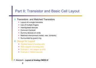
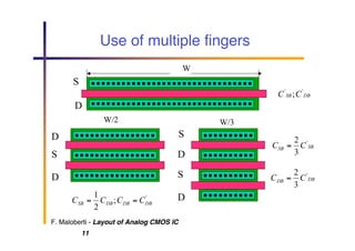
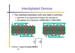
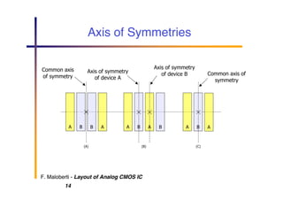
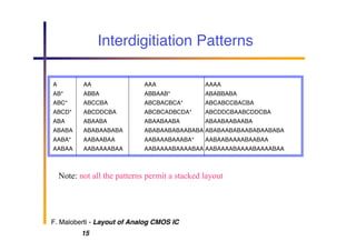
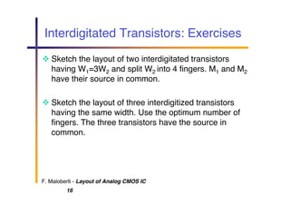
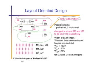
- Layout of a single transistor, use of multiple fingers, and interdigitated transistors for matching.
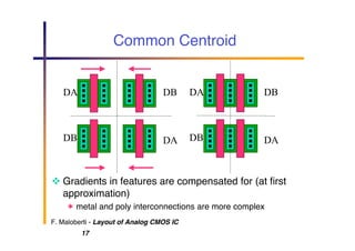
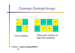
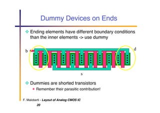
- Common centroid layouts and dummy devices to reduce mismatch.
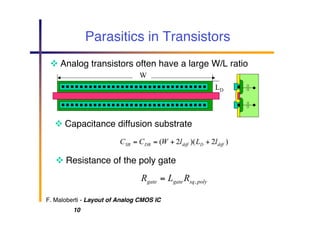
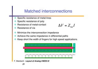
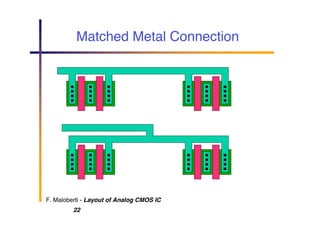
- Ensuring matched interconnect resistance, capacitance, and parasitics.
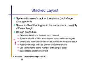
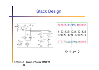
- Stacked layout of analog cells with stick diagrams to represent multiple transistors.
- Two examples of laying out basic cells - a two-stage op-amp and folded cascode. Design considerations like transistor sizing and grouping are discussed.


![Attack surfaces and attack tress[inform]](https://cdn.slidesharecdn.com/ss_thumbnails/lecture03-260108015941-a4dee53b-thumbnail.jpg?width=640&height=640&fit=bounds)

