2/24/2014
1
EE603 – CMOS IC DESIGN
Topic 5 – CMOS Inverter
Faizah Amir
POLISAS
TE
KN
OLOG
I
TE
RAS
PEM
BAN
GU
NAN
Lesson Learning Outcome
1) To explain the Switch Models of CMOS inverter
2) To explain the properties of static CMOS Inverter:
a. CMOS Voltage Transfer Characteristic (VTC)
b. Switching Threshold
c. Noise Margin
3) To explain the performance of static CMOS Inverter in
terms of:
a. Process Variation
b. Supply Voltage Scaling
4) To explain the dynamic behaviour of CMOS inverter
2/24/2014
2
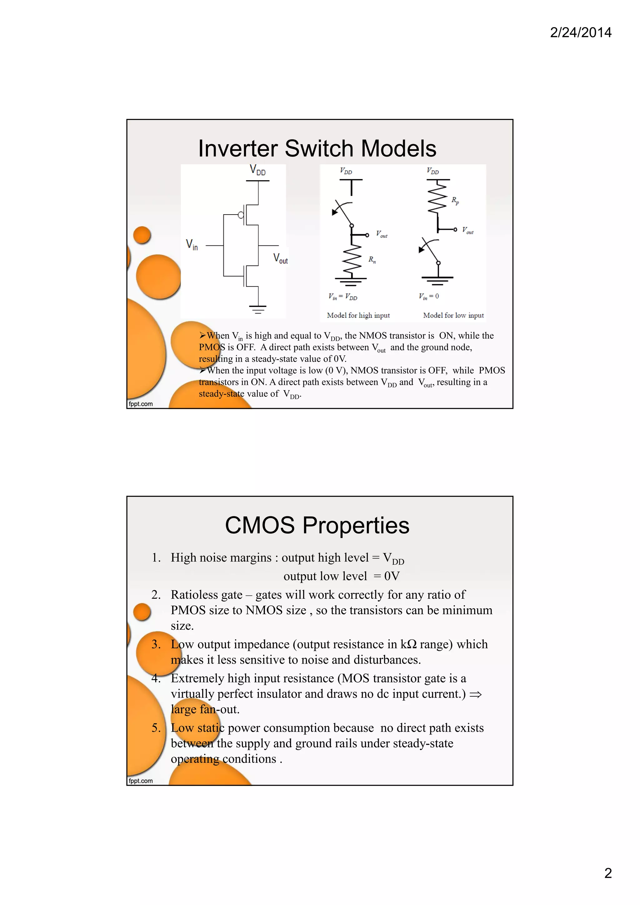
Inverter Switch Models
When Vin is high and equal to VDD, the NMOS transistor is ON, while the
PMOS is OFF. A direct path exists between Vout and the ground node,
resulting in a steady-state value of 0V.
When the input voltage is low (0 V), NMOS transistor is OFF, while PMOS
transistors in ON. A direct path exists between VDD and Vout, resulting in a
steady-state value of VDD.
CMOS Properties
1. High noise margins : output high level = VDD
output low level = 0V
2. Ratioless gate – gates will work correctly for any ratio of
PMOS size to NMOS size , so the transistors can be minimum
size.
3. Low output impedance (output resistance in kΩ range) which
makes it less sensitive to noise and disturbances.
4. Extremely high input resistance (MOS transistor gate is a
virtually perfect insulator and draws no dc input current.) ⇒
large fan-out.
5. Low static power consumption because no direct path exists
between the supply and ground rails under steady-state
operating conditions .
2/24/2014
3
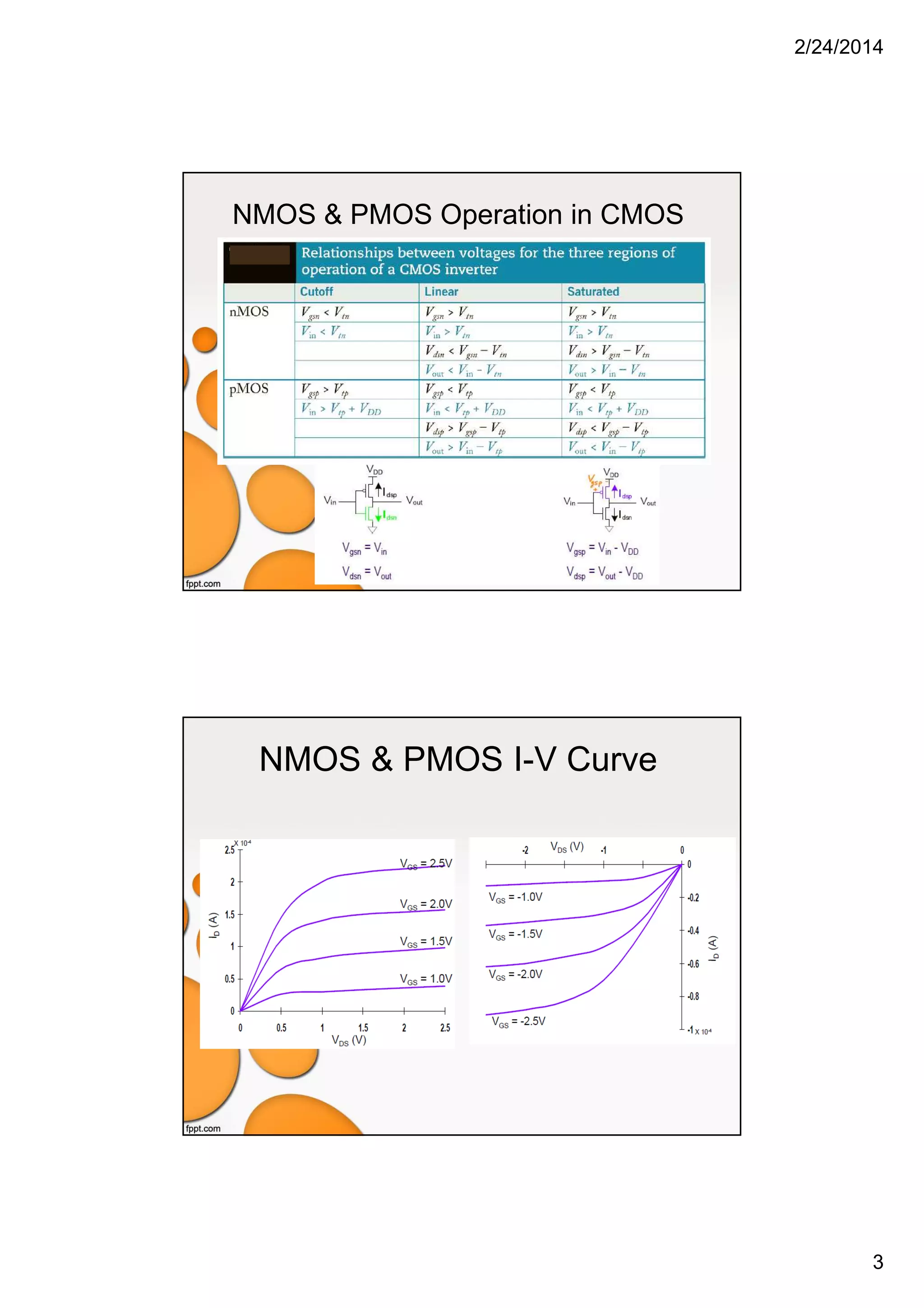
NMOS & PMOS Operation in CMOS
NMOS & PMOS I-V Curve
2/24/2014
4
NMOS & PMOS I-V Curve
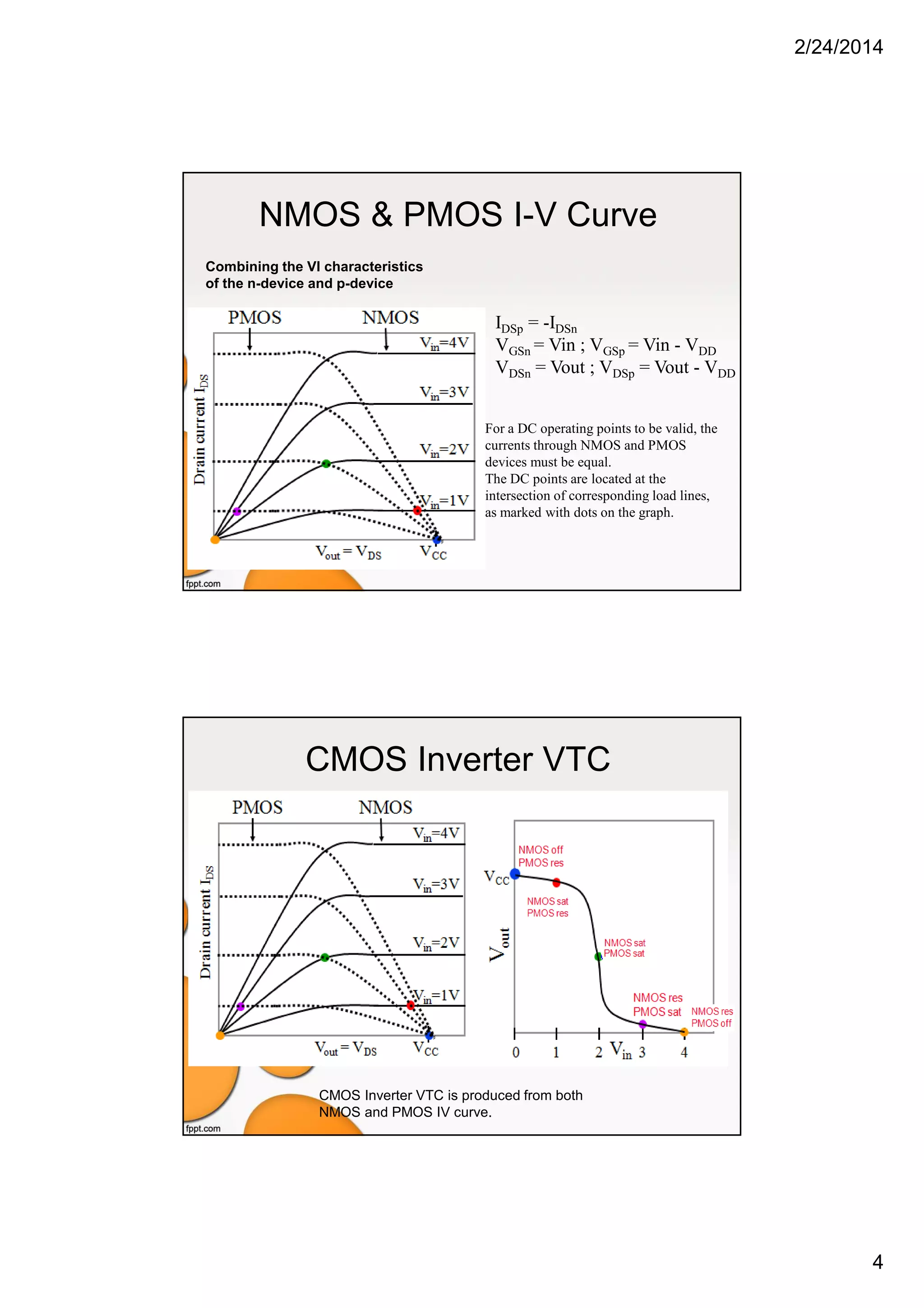
Combining the VI characteristics
of the n-device and p-device
IDSp = -IDSn
VGSn = Vin ; VGSp = Vin - VDD
VDSn = Vout ; VDSp = Vout - VDD
For a DC operating points to be valid, the
currents through NMOS and PMOS
devices must be equal.
The DC points are located at the
intersection of corresponding load lines,
as marked with dots on the graph.
CMOS Inverter VTC
CMOS Inverter VTC is produced from both
NMOS and PMOS IV curve.
2/24/2014
5
CMOS Inverter VTC
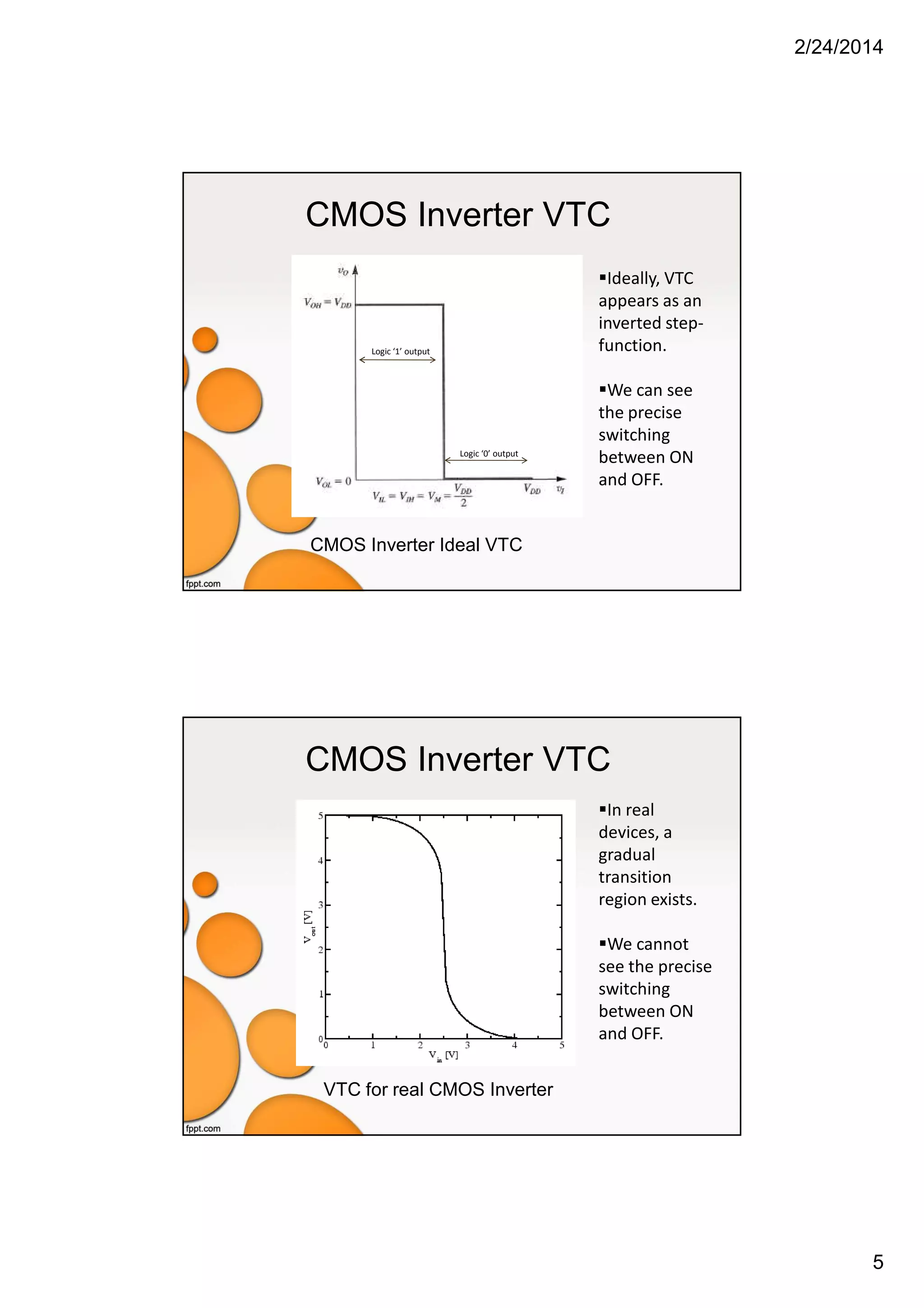
CMOS Inverter Ideal VTC
Ideally, VTC
appears as an
inverted step-
function.
We can see
the precise
switching
between ON
and OFF.
Logic ‘1’ output
Logic ‘0’ output
CMOS Inverter VTC
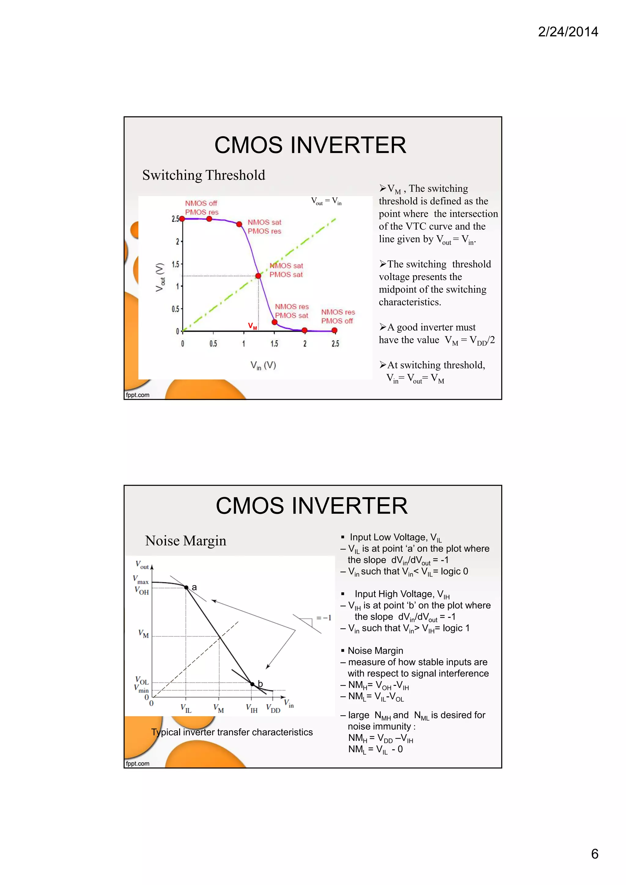
VTC for real CMOS Inverter
In real
devices, a
gradual
transition
region exists.
We cannot
see the precise
switching
between ON
and OFF.
2/24/2014
6
CMOS INVERTER
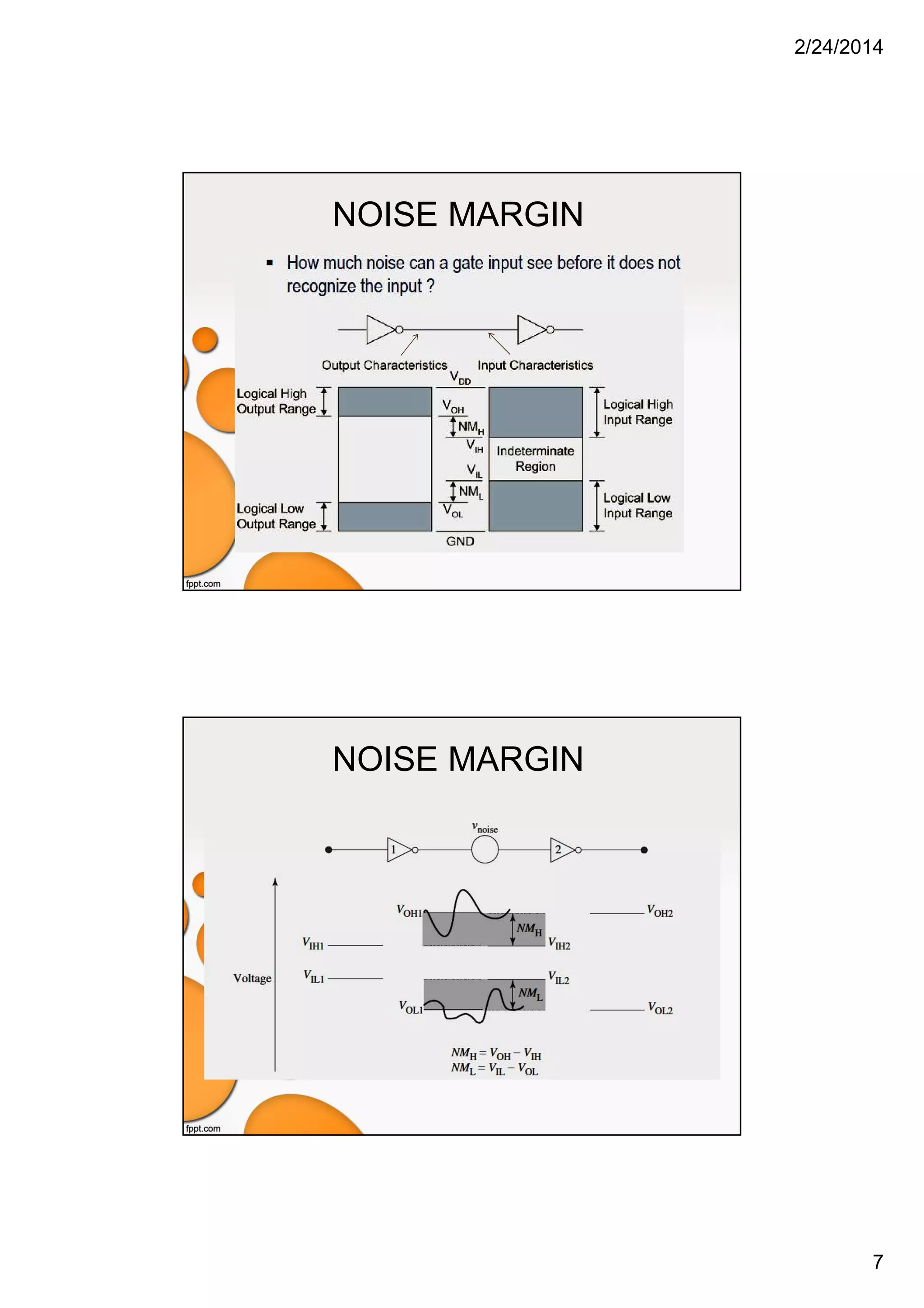
VM , The switching
threshold is defined as the
point where the intersection
of the VTC curve and the
line given by Vout = Vin.
The switching threshold
voltage presents the
midpoint of the switching
characteristics.
A good inverter must
have the value VM = VDD/2
At switching threshold,
Vin= Vout= VM
VM
Vout = Vin
Switching Threshold
CMOS INVERTER
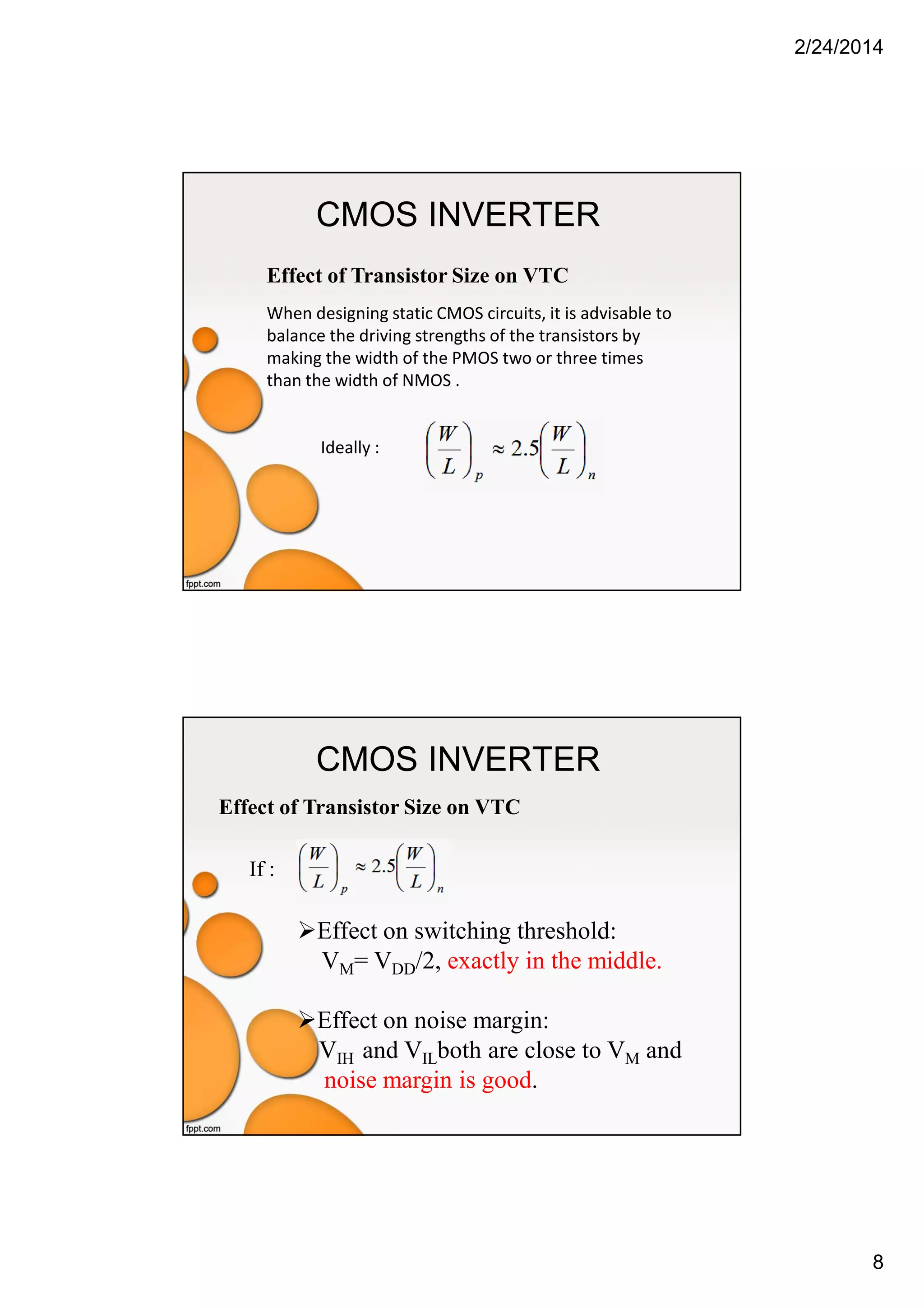
Noise Margin
Typical inverter transfer characteristics
Input Low Voltage, VIL
– VIL is at point ‘a’ on the plot where
the slope dVin/dVout = -1
– Vin such that Vin< VIL= logic 0
Input High Voltage, VIH
– VIH is at point ‘b’ on the plot where
the slope dVin/dVout = -1
– Vin such that Vin> VIH= logic 1
Noise Margin
– measure of how stable inputs are
with respect to signal interference
– NMH= VOH -VIH
– NML= VIL-VOL
– large NMH and NML is desired for
noise immunity :
NMH = VDD –VIH
NML = VIL - 0
● a
● b
2/24/2014
7
NOISE MARGIN
NOISE MARGIN
2/24/2014
8
CMOS INVERTER
Effect of Transistor Size on VTC
When designing static CMOS circuits, it is advisable to
balance the driving strengths of the transistors by
making the width of the PMOS two or three times
than the width of NMOS .
Ideally :
CMOS INVERTER
Effect of Transistor Size on VTC
Effect on switching threshold:
VM= VDD/2, exactly in the middle.
Effect on noise margin:
VIH and VILboth are close to VM and
noise margin is good.
If :
2/24/2014
9
CMOS INVERTER
Impact of process variation on VTC Curve
The “good” transistor has:
smaller oxide thickness
smaller length
higher width
smaller threshold voltage
The “bad” transistor has:
larger oxide thickness
larger length
lower width
larger threshold voltage
Conclusion:
The variations cause a small shift
in the switching threshold, but that
the operation of the gate is not
affected.
Process variations (mostly) cause a
shift in the switching threshold.
●●
●
CMOS INVERTER
Impact of process variation on VTC Curve
Result from changing (W/L)p / (W/L)n ratio:
• Inverter threshold VM ≠ VDD/2
• Rise and fall delays are unequal
• Noise margins are not equal
2/24/2014
10
CMOS INVERTER
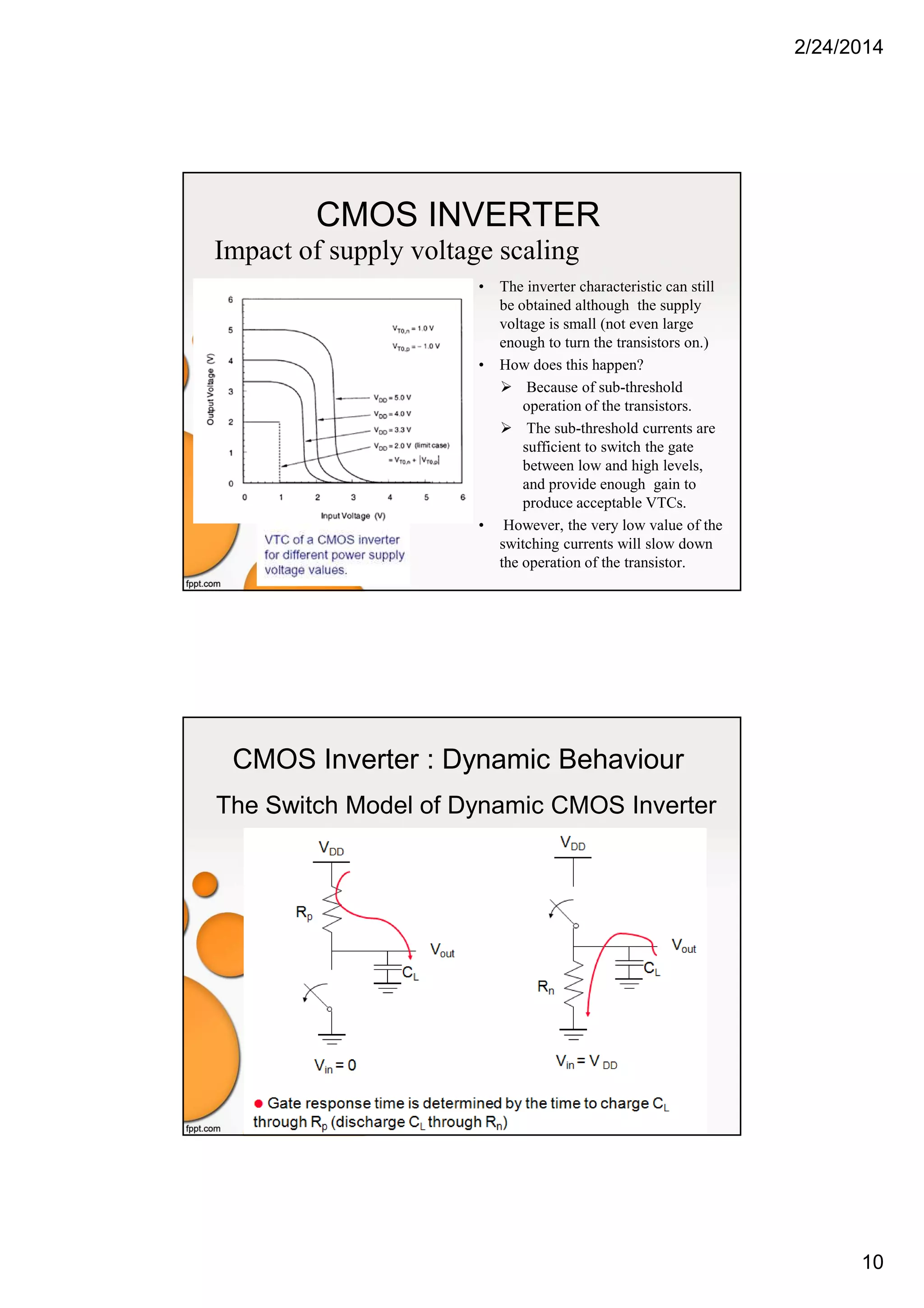
Impact of supply voltage scaling
• The inverter characteristic can still
be obtained although the supply
voltage is small (not even large
enough to turn the transistors on.)
• How does this happen?
Because of sub-threshold
operation of the transistors.
The sub-threshold currents are
sufficient to switch the gate
between low and high levels,
and provide enough gain to
produce acceptable VTCs.
• However, the very low value of the
switching currents will slow down
the operation of the transistor.
CMOS Inverter : Dynamic Behaviour
The Switch Model of Dynamic CMOS Inverter
2/24/2014
11
CMOS Inverter : Dynamic Behaviour
Parasitic Capacitances of CMOS inverter
Parasitic capacitances, influencing the transient behaviour of
the cascaded inverter pair.
CMOS Inverter : Dynamic Behaviour
Parasitic Capacitances – Miller Effect
The Miller effect— A capacitor that has identical but opposite
voltage swings at both its terminals can be replaced by a capacitor
to ground, whose value is two times the original value.
2/24/2014
12
CMOS Inverter : Dynamic Behaviour
Sources of parasitic capacitance:
i. Intrinsic MOS transistor capacitances
ii. Extrinsic MOS transistor (fan-out)
capacitances
iii. Wiring (interconnect) capacitance
Sources of Parasitic Capacitances
• MOS Intrinsic Capacitances
Structure capacitances
Channel capacitances
Diffusion capacitances
2/24/2014
13
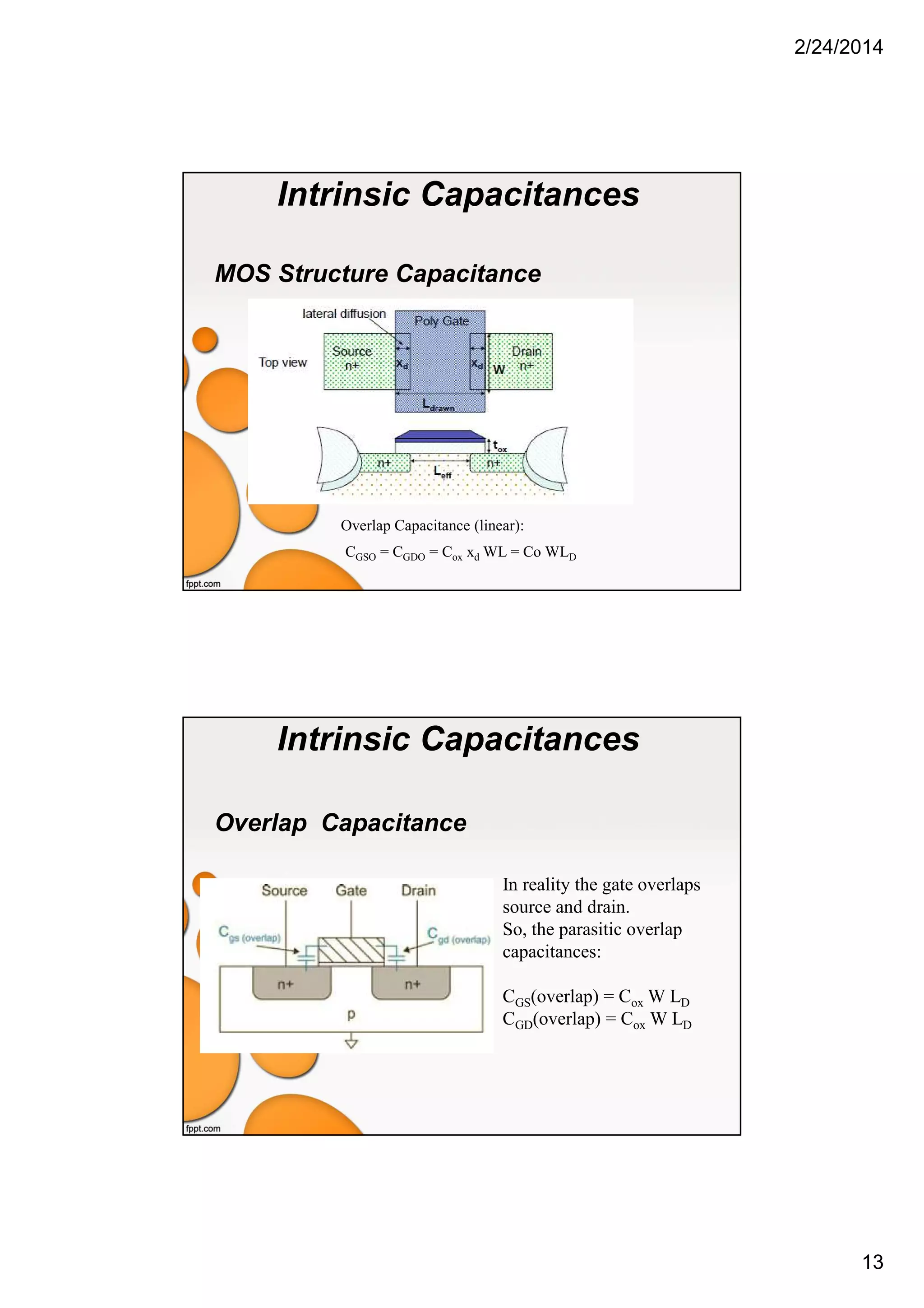
Intrinsic Capacitances
MOS Structure Capacitance
Overlap Capacitance (linear):
CGSO = CGDO = Cox xd WL = Co WLD
Intrinsic Capacitances
Overlap Capacitance
In reality the gate overlaps
source and drain.
So, the parasitic overlap
capacitances:
CGS(overlap) = Cox W LD
CGD(overlap) = Cox W LD
2/24/2014
14
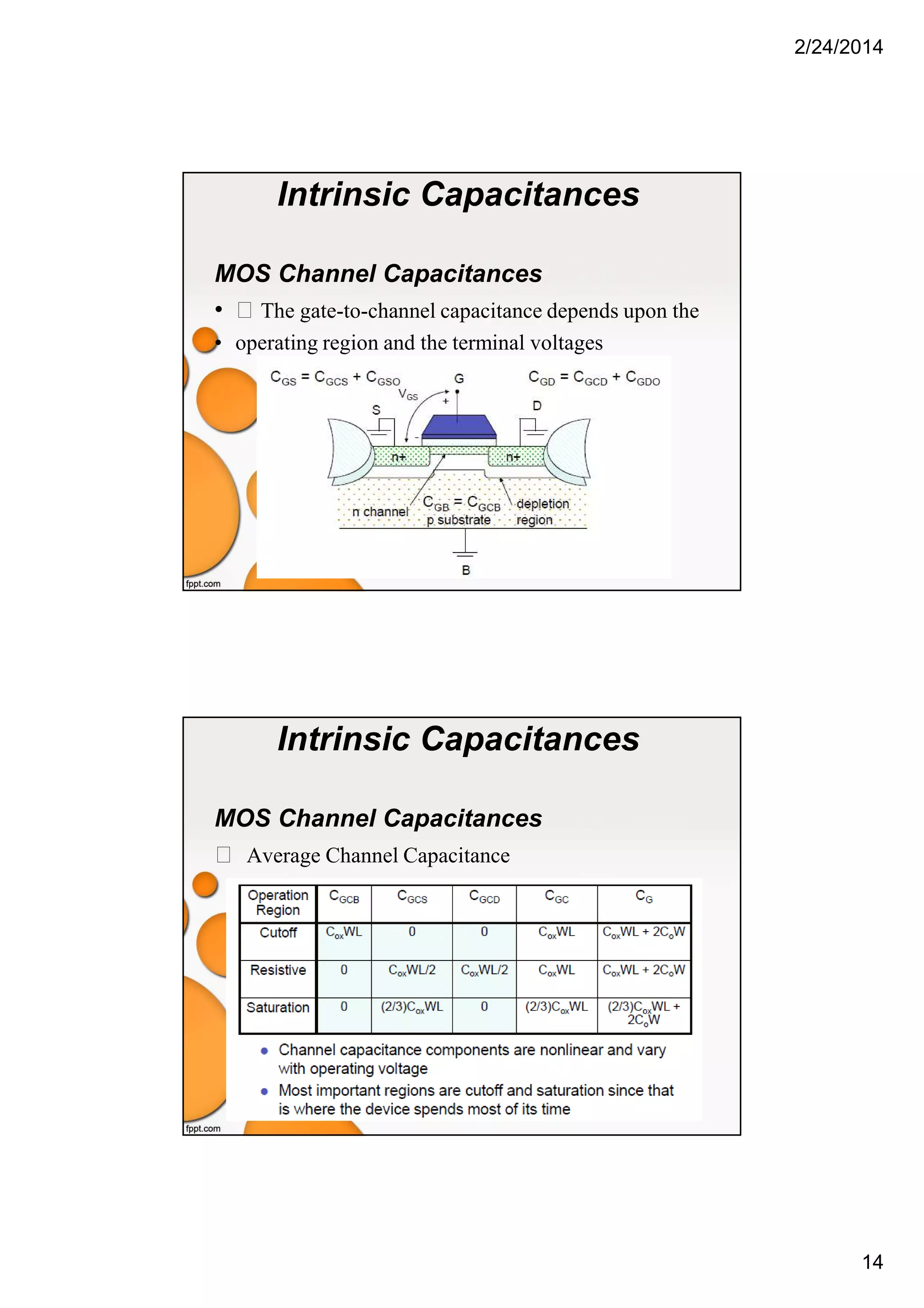
Intrinsic Capacitances
MOS Channel Capacitances
• The gate-to-channel capacitance depends upon the
• operating region and the terminal voltages
Intrinsic Capacitances
MOS Channel Capacitances
Average Channel Capacitance
2/24/2014
15
Intrinsic Capacitances
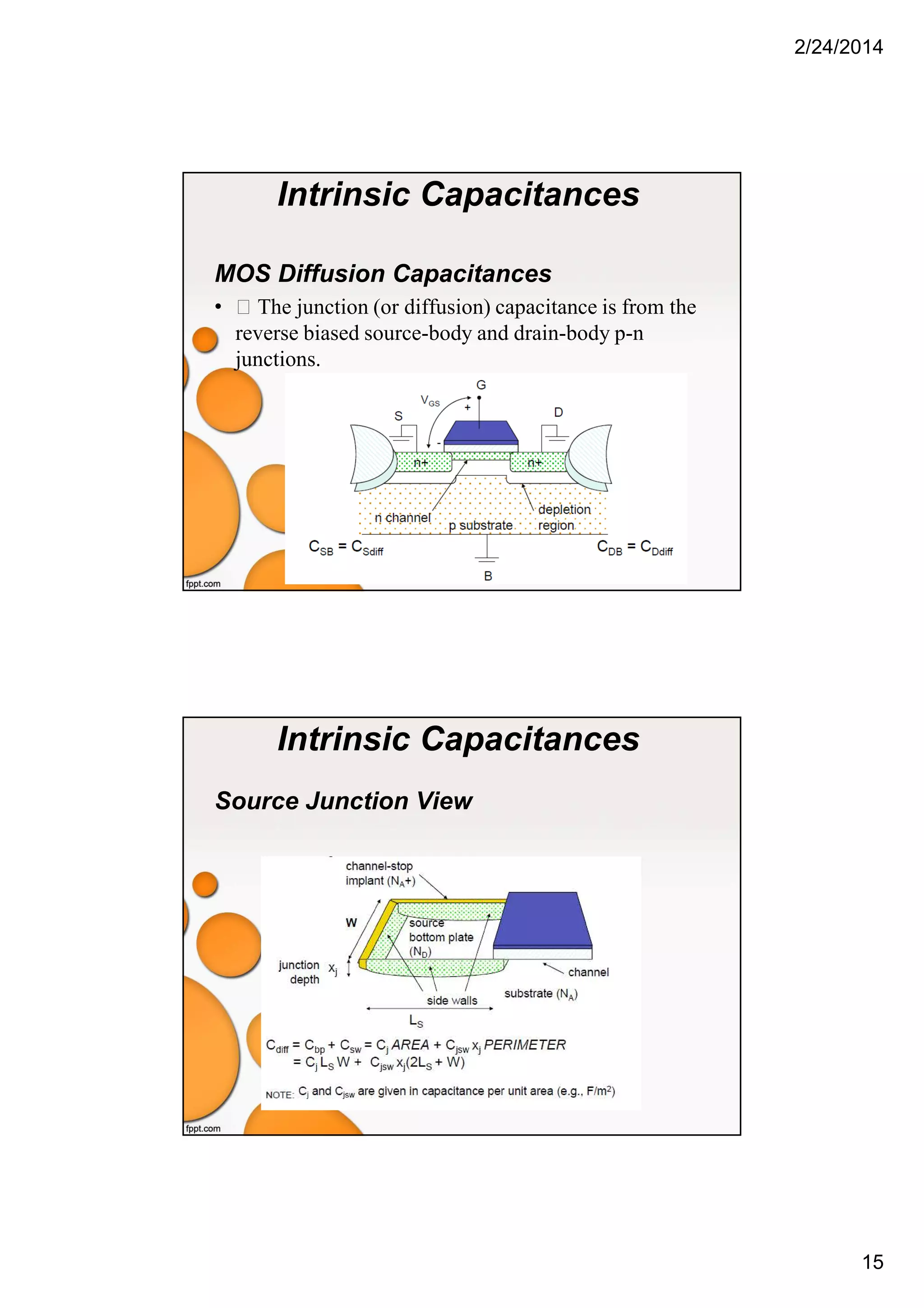
MOS Diffusion Capacitances
• The junction (or diffusion) capacitance is from the
reverse biased source-body and drain-body p-n
junctions.
Intrinsic Capacitances
Source Junction View
2/24/2014
16
Extrinsic Capacitance
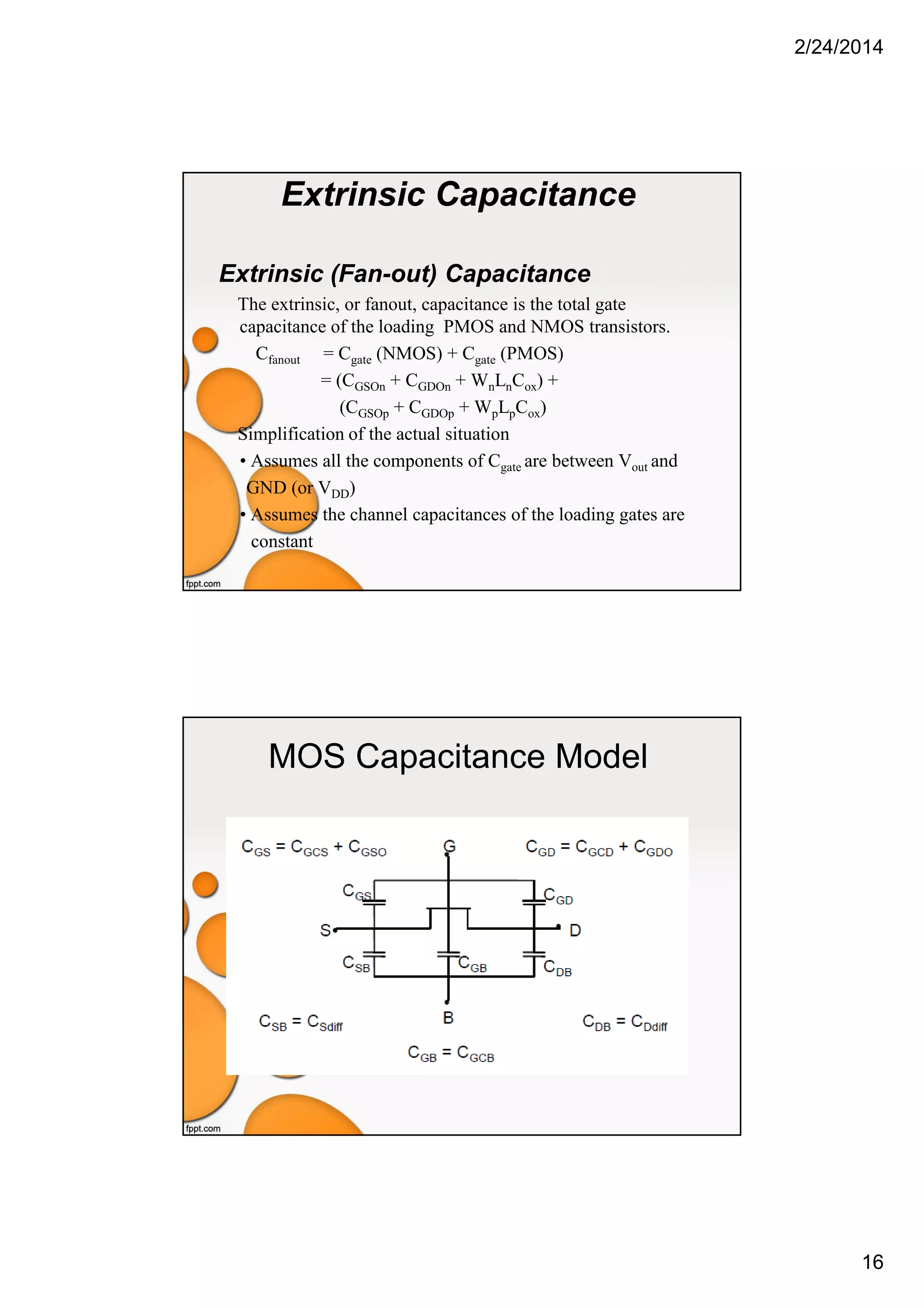
Extrinsic (Fan-out) Capacitance
The extrinsic, or fanout, capacitance is the total gate
capacitance of the loading PMOS and NMOS transistors.
Cfanout = Cgate (NMOS) + Cgate (PMOS)
= (CGSOn + CGDOn + WnLnCox) +
(CGSOp + CGDOp + WpLpCox)
Simplification of the actual situation
• Assumes all the components of Cgate are between Vout and
GND (or VDD)
• Assumes the channel capacitances of the loading gates are
constant
MOS Capacitance Model
2/24/2014
17
Summary
1. When designing static CMOS circuits, the width of PMOS
must be made two or three times than the width of NMOS
in order to obtain symmetrical switching threshold, VM and
noise margin.
2. The variations of NMOS and PMOS in CMOS cause a small
shift in the switching threshold, but that the operation of the
gate is not affected.
3. The inverter characteristic can still be obtained although the
supply voltage is scaled down, as long as the minimum
supply voltage is higher than thermal voltage
4. Parasitic capacitances slower the switching speeds
=>Bigger capacitance means more charges are needed to change
voltage.
Past Years Questions
1. a) Sketch a complete CMOS inverter circuit diagram.
(2 marks)
2. Explain the CMOS inverter operation.
(2 marks)
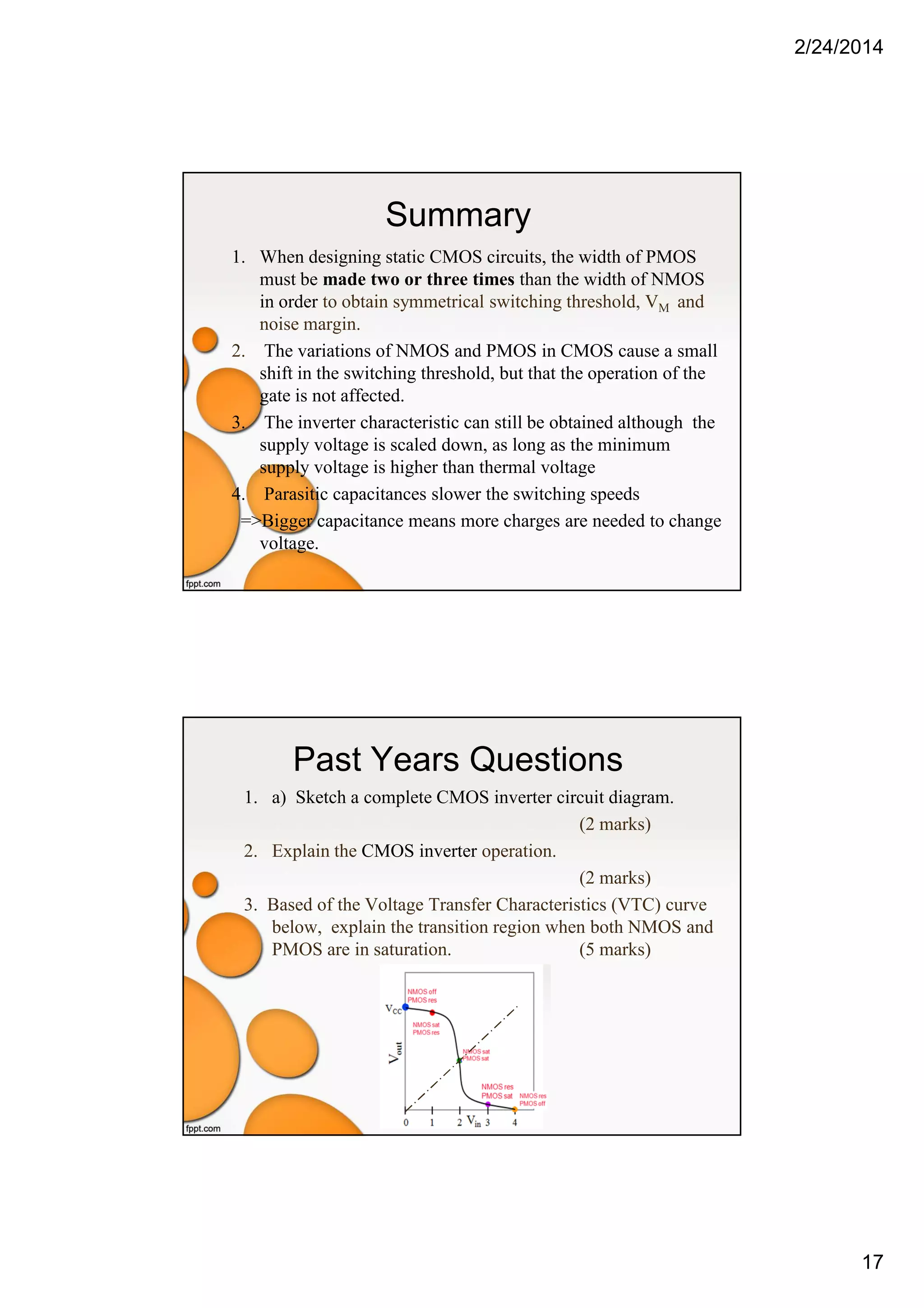
3. Based of the Voltage Transfer Characteristics (VTC) curve
below, explain the transition region when both NMOS and
PMOS are in saturation. (5 marks)
2/24/2014
18

CMOS Topic 5 -_cmos_inverter

  • 1.
    2/24/2014 1 EE603 – CMOSIC DESIGN Topic 5 – CMOS Inverter Faizah Amir POLISAS TE KN OLOG I TE RAS PEM BAN GU NAN Lesson Learning Outcome 1) To explain the Switch Models of CMOS inverter 2) To explain the properties of static CMOS Inverter: a. CMOS Voltage Transfer Characteristic (VTC) b. Switching Threshold c. Noise Margin 3) To explain the performance of static CMOS Inverter in terms of: a. Process Variation b. Supply Voltage Scaling 4) To explain the dynamic behaviour of CMOS inverter
  • 2.
    2/24/2014 2 Inverter Switch Models WhenVin is high and equal to VDD, the NMOS transistor is ON, while the PMOS is OFF. A direct path exists between Vout and the ground node, resulting in a steady-state value of 0V. When the input voltage is low (0 V), NMOS transistor is OFF, while PMOS transistors in ON. A direct path exists between VDD and Vout, resulting in a steady-state value of VDD. CMOS Properties 1. High noise margins : output high level = VDD output low level = 0V 2. Ratioless gate – gates will work correctly for any ratio of PMOS size to NMOS size , so the transistors can be minimum size. 3. Low output impedance (output resistance in kΩ range) which makes it less sensitive to noise and disturbances. 4. Extremely high input resistance (MOS transistor gate is a virtually perfect insulator and draws no dc input current.) ⇒ large fan-out. 5. Low static power consumption because no direct path exists between the supply and ground rails under steady-state operating conditions .
  • 3.
    2/24/2014 3 NMOS & PMOSOperation in CMOS NMOS & PMOS I-V Curve
  • 4.
    2/24/2014 4 NMOS & PMOSI-V Curve Combining the VI characteristics of the n-device and p-device IDSp = -IDSn VGSn = Vin ; VGSp = Vin - VDD VDSn = Vout ; VDSp = Vout - VDD For a DC operating points to be valid, the currents through NMOS and PMOS devices must be equal. The DC points are located at the intersection of corresponding load lines, as marked with dots on the graph. CMOS Inverter VTC CMOS Inverter VTC is produced from both NMOS and PMOS IV curve.
  • 5.
    2/24/2014 5 CMOS Inverter VTC CMOSInverter Ideal VTC Ideally, VTC appears as an inverted step- function. We can see the precise switching between ON and OFF. Logic ‘1’ output Logic ‘0’ output CMOS Inverter VTC VTC for real CMOS Inverter In real devices, a gradual transition region exists. We cannot see the precise switching between ON and OFF.
  • 6.
    2/24/2014 6 CMOS INVERTER VM ,The switching threshold is defined as the point where the intersection of the VTC curve and the line given by Vout = Vin. The switching threshold voltage presents the midpoint of the switching characteristics. A good inverter must have the value VM = VDD/2 At switching threshold, Vin= Vout= VM VM Vout = Vin Switching Threshold CMOS INVERTER Noise Margin Typical inverter transfer characteristics Input Low Voltage, VIL – VIL is at point ‘a’ on the plot where the slope dVin/dVout = -1 – Vin such that Vin< VIL= logic 0 Input High Voltage, VIH – VIH is at point ‘b’ on the plot where the slope dVin/dVout = -1 – Vin such that Vin> VIH= logic 1 Noise Margin – measure of how stable inputs are with respect to signal interference – NMH= VOH -VIH – NML= VIL-VOL – large NMH and NML is desired for noise immunity : NMH = VDD –VIH NML = VIL - 0 ● a ● b
  • 7.
  • 8.
    2/24/2014 8 CMOS INVERTER Effect ofTransistor Size on VTC When designing static CMOS circuits, it is advisable to balance the driving strengths of the transistors by making the width of the PMOS two or three times than the width of NMOS . Ideally : CMOS INVERTER Effect of Transistor Size on VTC Effect on switching threshold: VM= VDD/2, exactly in the middle. Effect on noise margin: VIH and VILboth are close to VM and noise margin is good. If :
  • 9.
    2/24/2014 9 CMOS INVERTER Impact ofprocess variation on VTC Curve The “good” transistor has: smaller oxide thickness smaller length higher width smaller threshold voltage The “bad” transistor has: larger oxide thickness larger length lower width larger threshold voltage Conclusion: The variations cause a small shift in the switching threshold, but that the operation of the gate is not affected. Process variations (mostly) cause a shift in the switching threshold. ●● ● CMOS INVERTER Impact of process variation on VTC Curve Result from changing (W/L)p / (W/L)n ratio: • Inverter threshold VM ≠ VDD/2 • Rise and fall delays are unequal • Noise margins are not equal
  • 10.
    2/24/2014 10 CMOS INVERTER Impact ofsupply voltage scaling • The inverter characteristic can still be obtained although the supply voltage is small (not even large enough to turn the transistors on.) • How does this happen? Because of sub-threshold operation of the transistors. The sub-threshold currents are sufficient to switch the gate between low and high levels, and provide enough gain to produce acceptable VTCs. • However, the very low value of the switching currents will slow down the operation of the transistor. CMOS Inverter : Dynamic Behaviour The Switch Model of Dynamic CMOS Inverter
  • 11.
    2/24/2014 11 CMOS Inverter :Dynamic Behaviour Parasitic Capacitances of CMOS inverter Parasitic capacitances, influencing the transient behaviour of the cascaded inverter pair. CMOS Inverter : Dynamic Behaviour Parasitic Capacitances – Miller Effect The Miller effect— A capacitor that has identical but opposite voltage swings at both its terminals can be replaced by a capacitor to ground, whose value is two times the original value.
  • 12.
    2/24/2014 12 CMOS Inverter :Dynamic Behaviour Sources of parasitic capacitance: i. Intrinsic MOS transistor capacitances ii. Extrinsic MOS transistor (fan-out) capacitances iii. Wiring (interconnect) capacitance Sources of Parasitic Capacitances • MOS Intrinsic Capacitances Structure capacitances Channel capacitances Diffusion capacitances
  • 13.
    2/24/2014 13 Intrinsic Capacitances MOS StructureCapacitance Overlap Capacitance (linear): CGSO = CGDO = Cox xd WL = Co WLD Intrinsic Capacitances Overlap Capacitance In reality the gate overlaps source and drain. So, the parasitic overlap capacitances: CGS(overlap) = Cox W LD CGD(overlap) = Cox W LD
  • 14.
    2/24/2014 14 Intrinsic Capacitances MOS ChannelCapacitances • The gate-to-channel capacitance depends upon the • operating region and the terminal voltages Intrinsic Capacitances MOS Channel Capacitances Average Channel Capacitance
  • 15.
    2/24/2014 15 Intrinsic Capacitances MOS DiffusionCapacitances • The junction (or diffusion) capacitance is from the reverse biased source-body and drain-body p-n junctions. Intrinsic Capacitances Source Junction View
  • 16.
    2/24/2014 16 Extrinsic Capacitance Extrinsic (Fan-out)Capacitance The extrinsic, or fanout, capacitance is the total gate capacitance of the loading PMOS and NMOS transistors. Cfanout = Cgate (NMOS) + Cgate (PMOS) = (CGSOn + CGDOn + WnLnCox) + (CGSOp + CGDOp + WpLpCox) Simplification of the actual situation • Assumes all the components of Cgate are between Vout and GND (or VDD) • Assumes the channel capacitances of the loading gates are constant MOS Capacitance Model
  • 17.
    2/24/2014 17 Summary 1. When designingstatic CMOS circuits, the width of PMOS must be made two or three times than the width of NMOS in order to obtain symmetrical switching threshold, VM and noise margin. 2. The variations of NMOS and PMOS in CMOS cause a small shift in the switching threshold, but that the operation of the gate is not affected. 3. The inverter characteristic can still be obtained although the supply voltage is scaled down, as long as the minimum supply voltage is higher than thermal voltage 4. Parasitic capacitances slower the switching speeds =>Bigger capacitance means more charges are needed to change voltage. Past Years Questions 1. a) Sketch a complete CMOS inverter circuit diagram. (2 marks) 2. Explain the CMOS inverter operation. (2 marks) 3. Based of the Voltage Transfer Characteristics (VTC) curve below, explain the transition region when both NMOS and PMOS are in saturation. (5 marks)
  • 18.