Downloaded 129 times


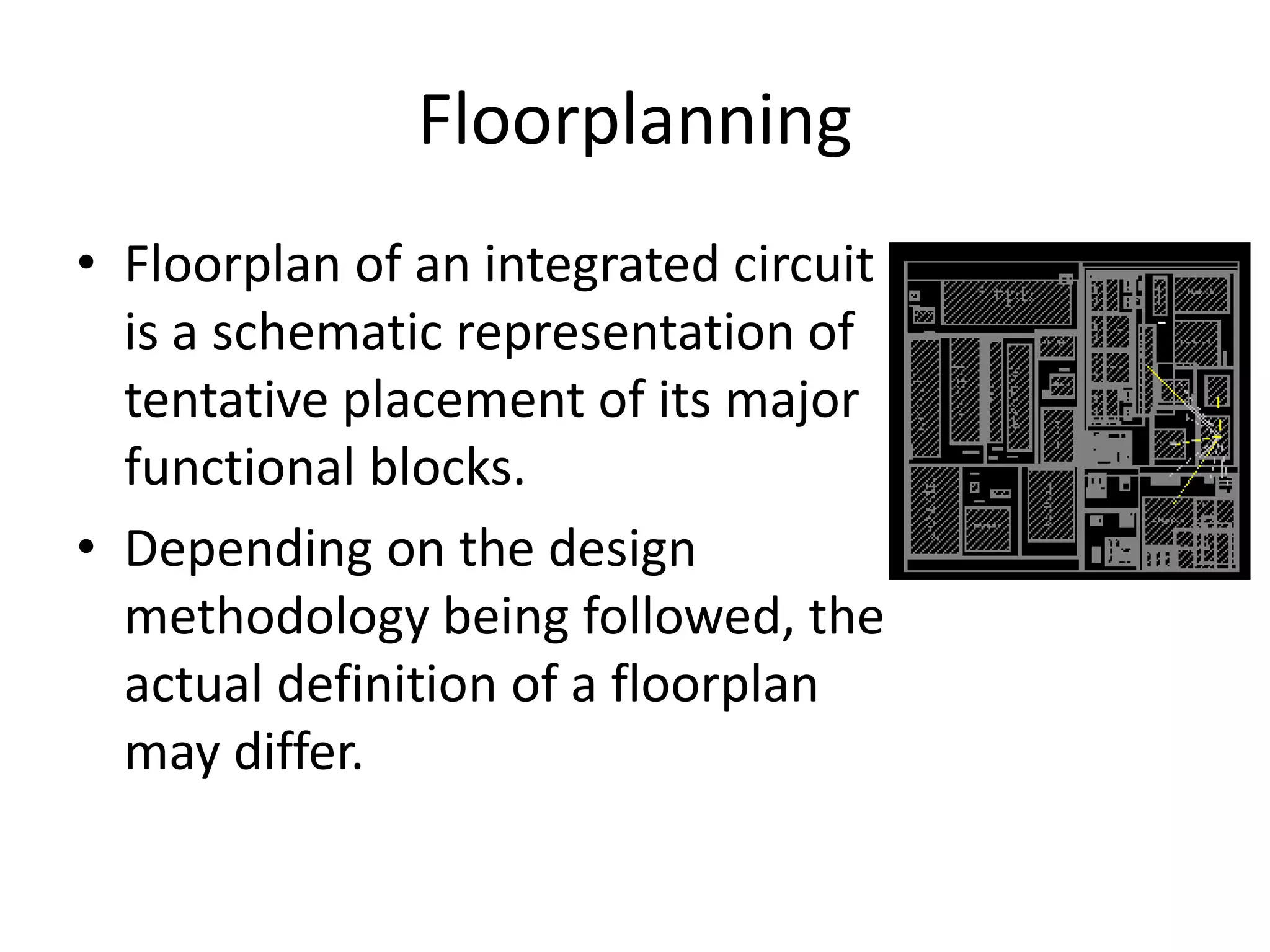

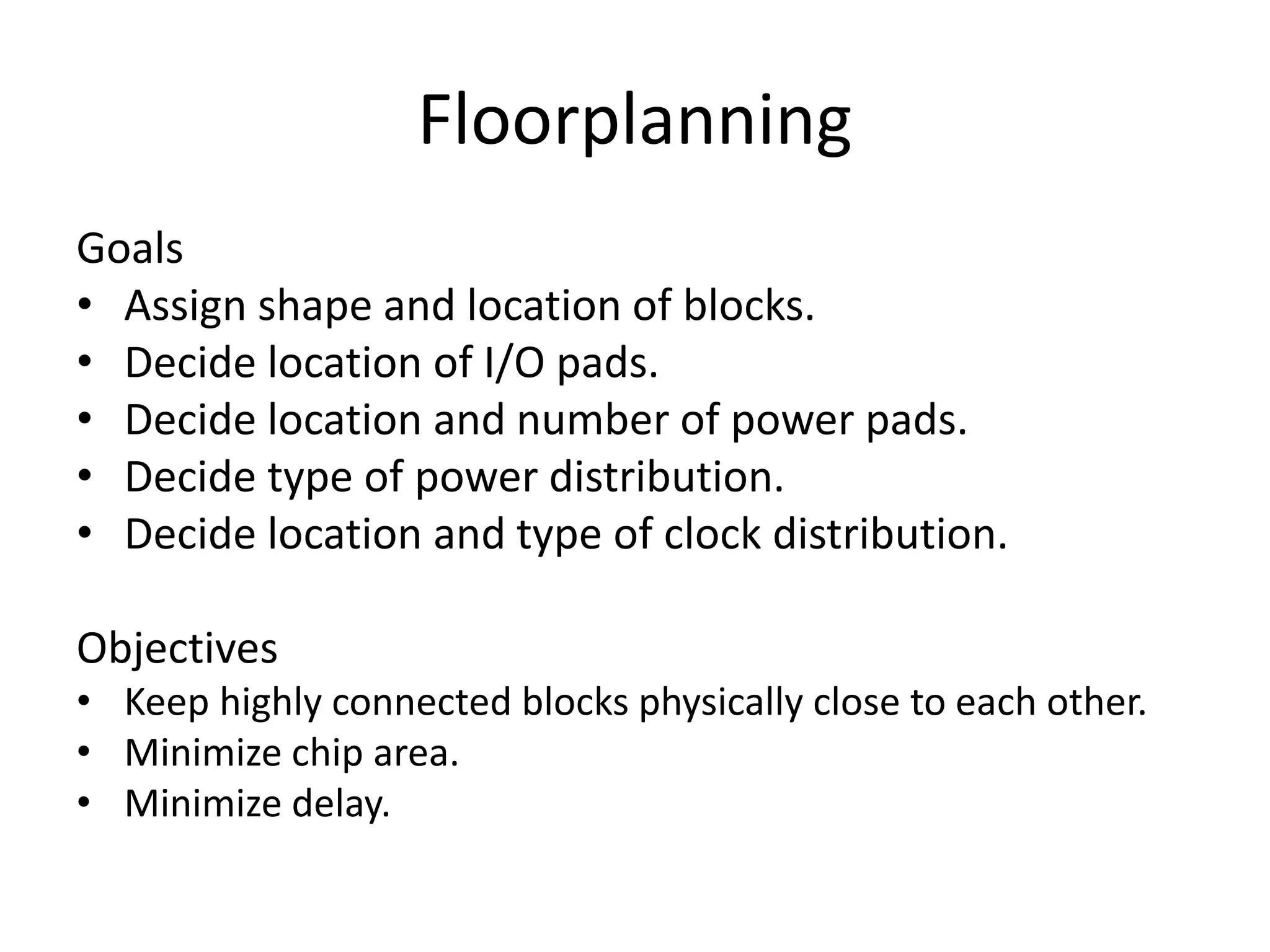
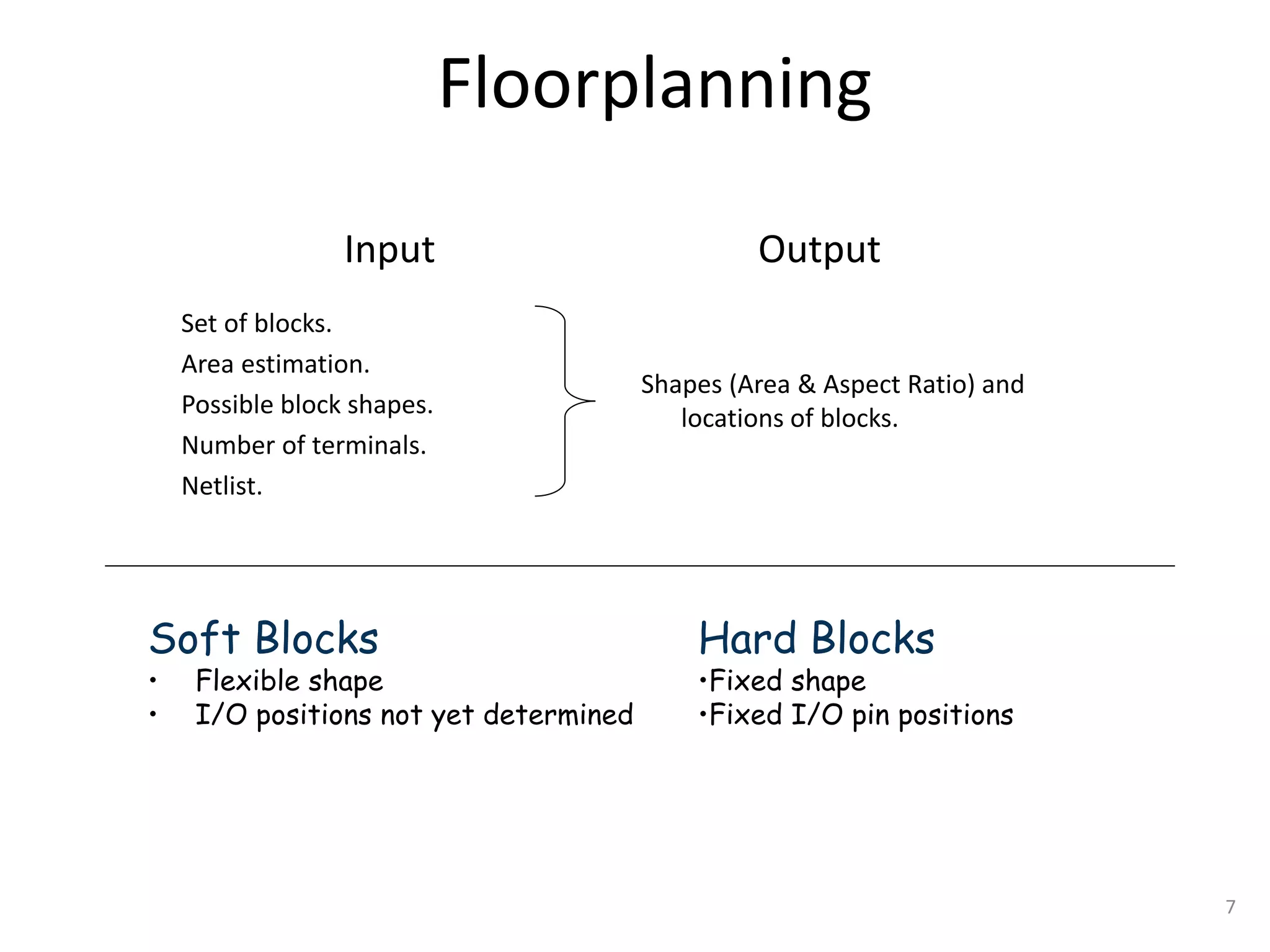
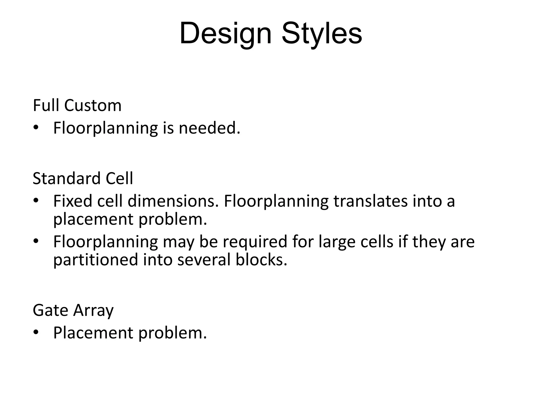

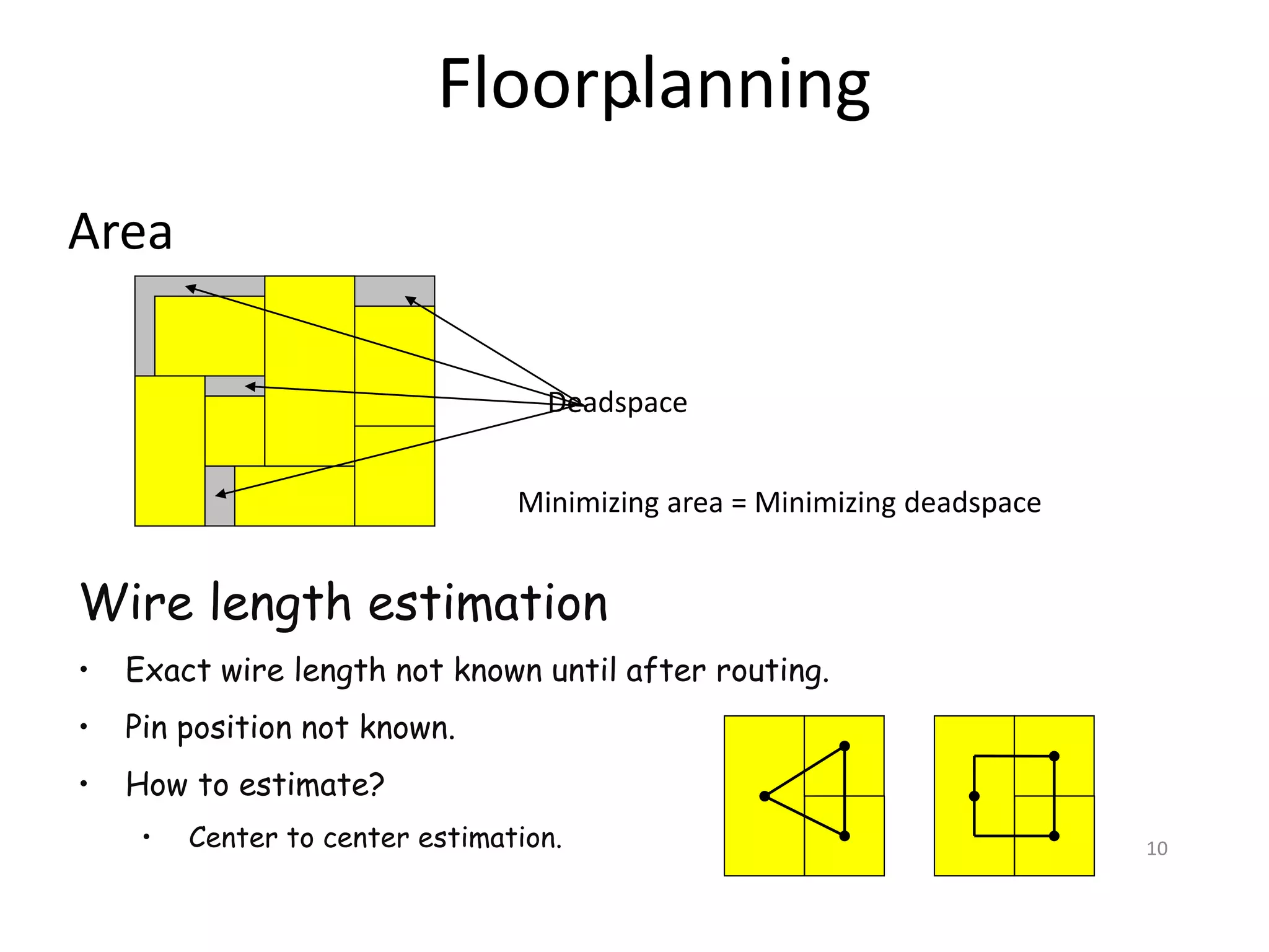


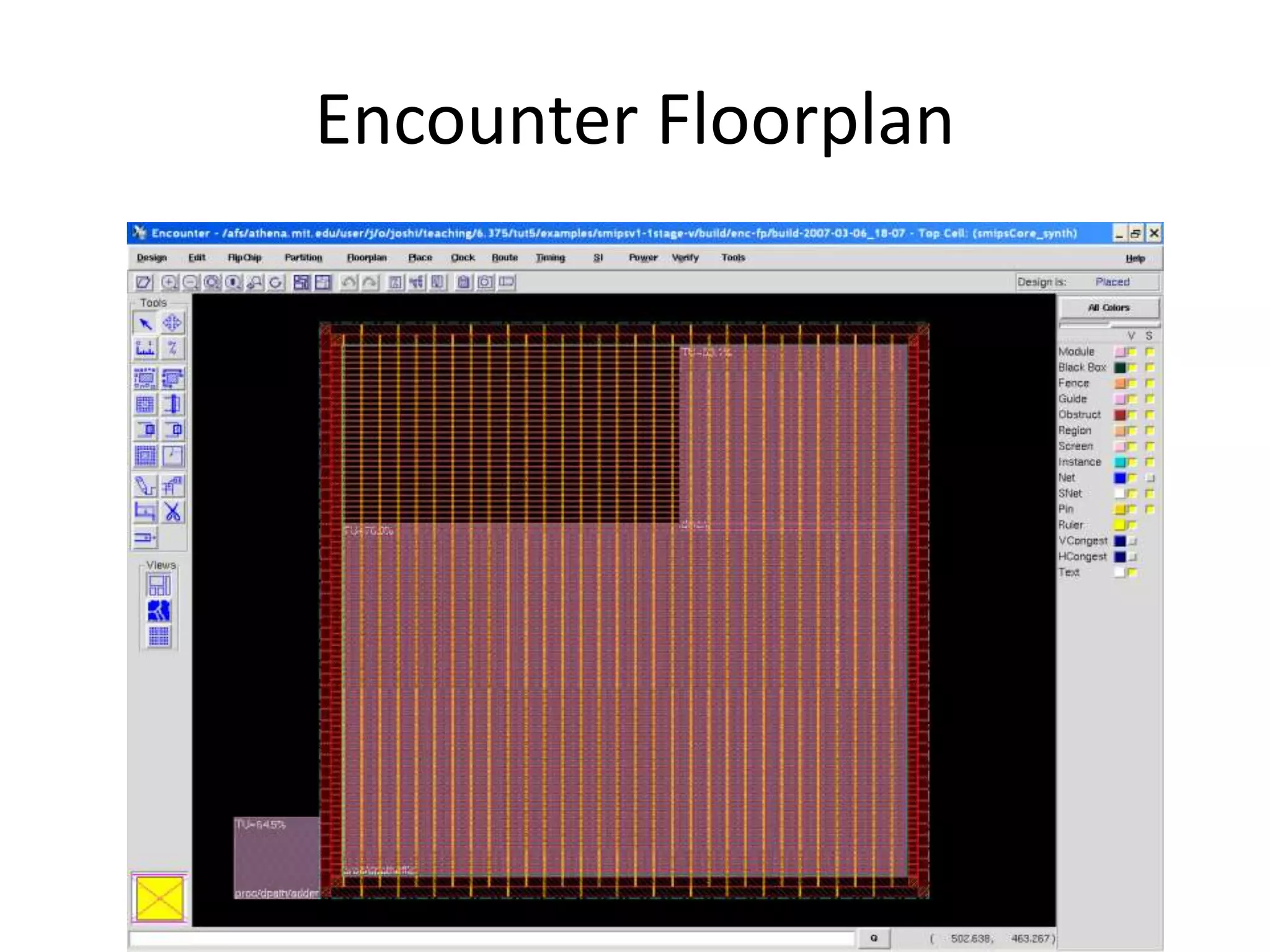


The document discusses floorplanning in integrated circuit design. Floorplanning involves tentatively placing functional blocks on a chip to optimize the design for area, wirelength, delay and other factors like noise and heat dissipation. It describes the goals and inputs/outputs of floorplanning. Floorplanning styles can be slicing, non-slicing, full custom, standard cell or gate array. Algorithms used for floorplanning include Stockmeyer, simulated annealing, linear programming and sequence-pair based approaches. Floorplans can be represented by normalized polish expressions.