Downloaded 1,126 times
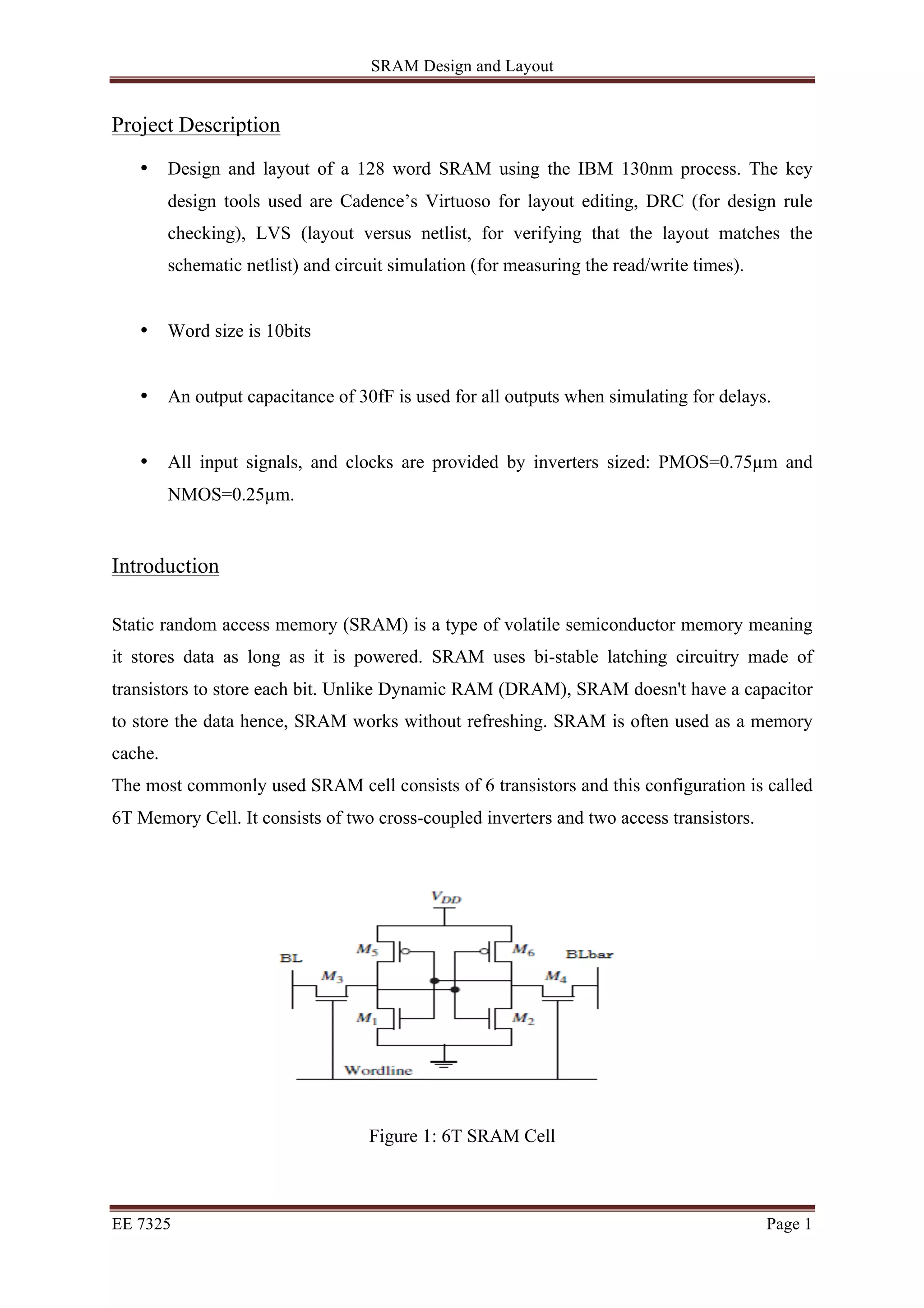
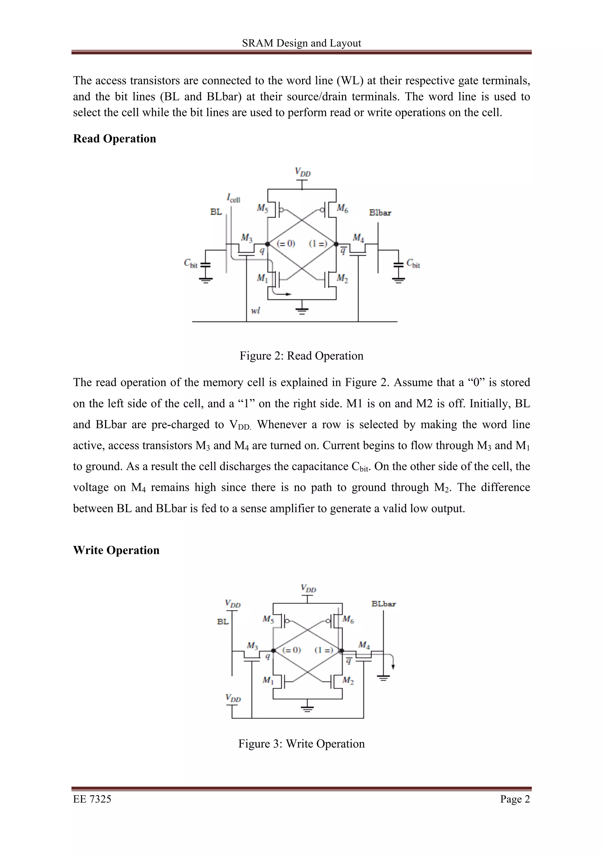
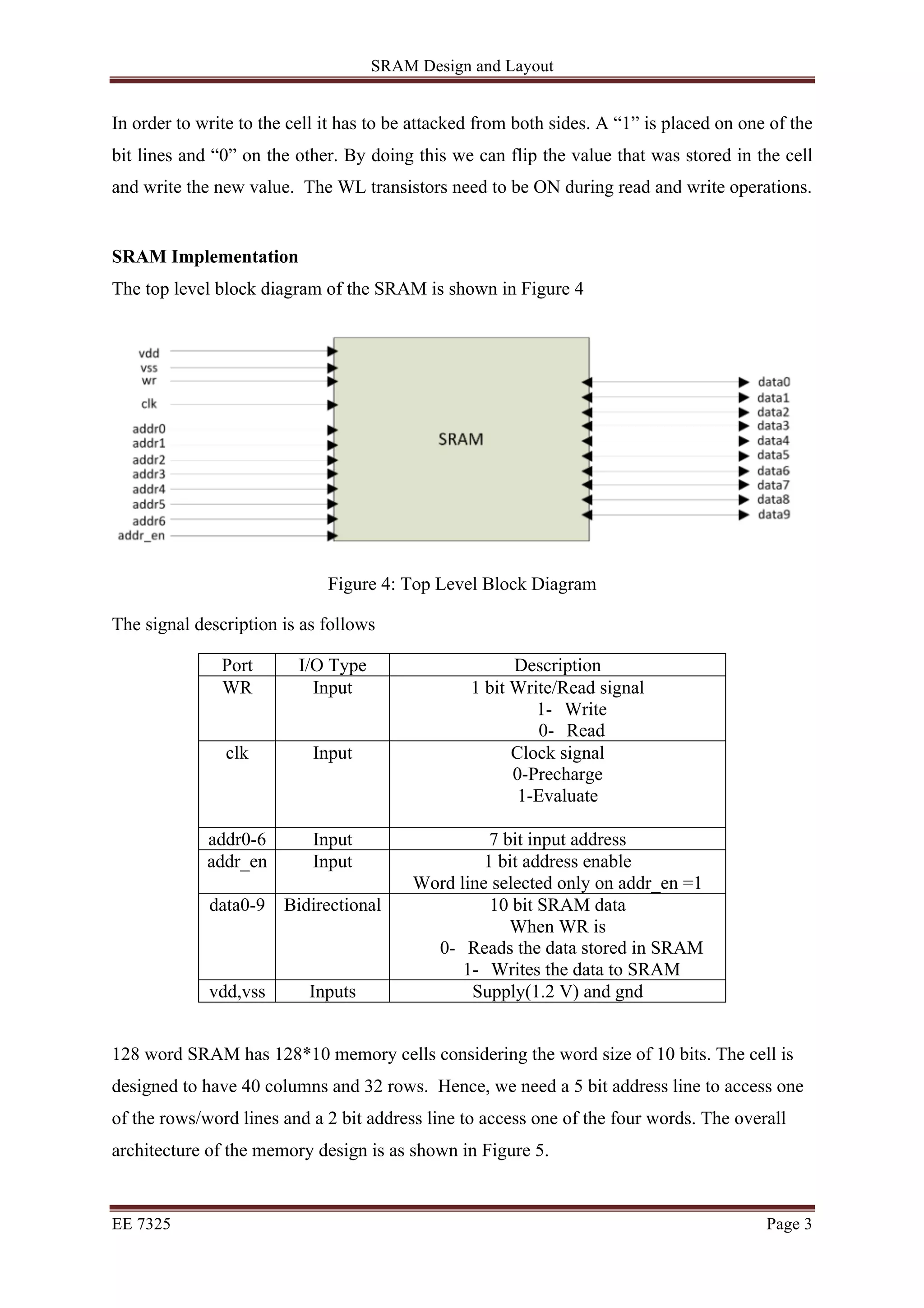
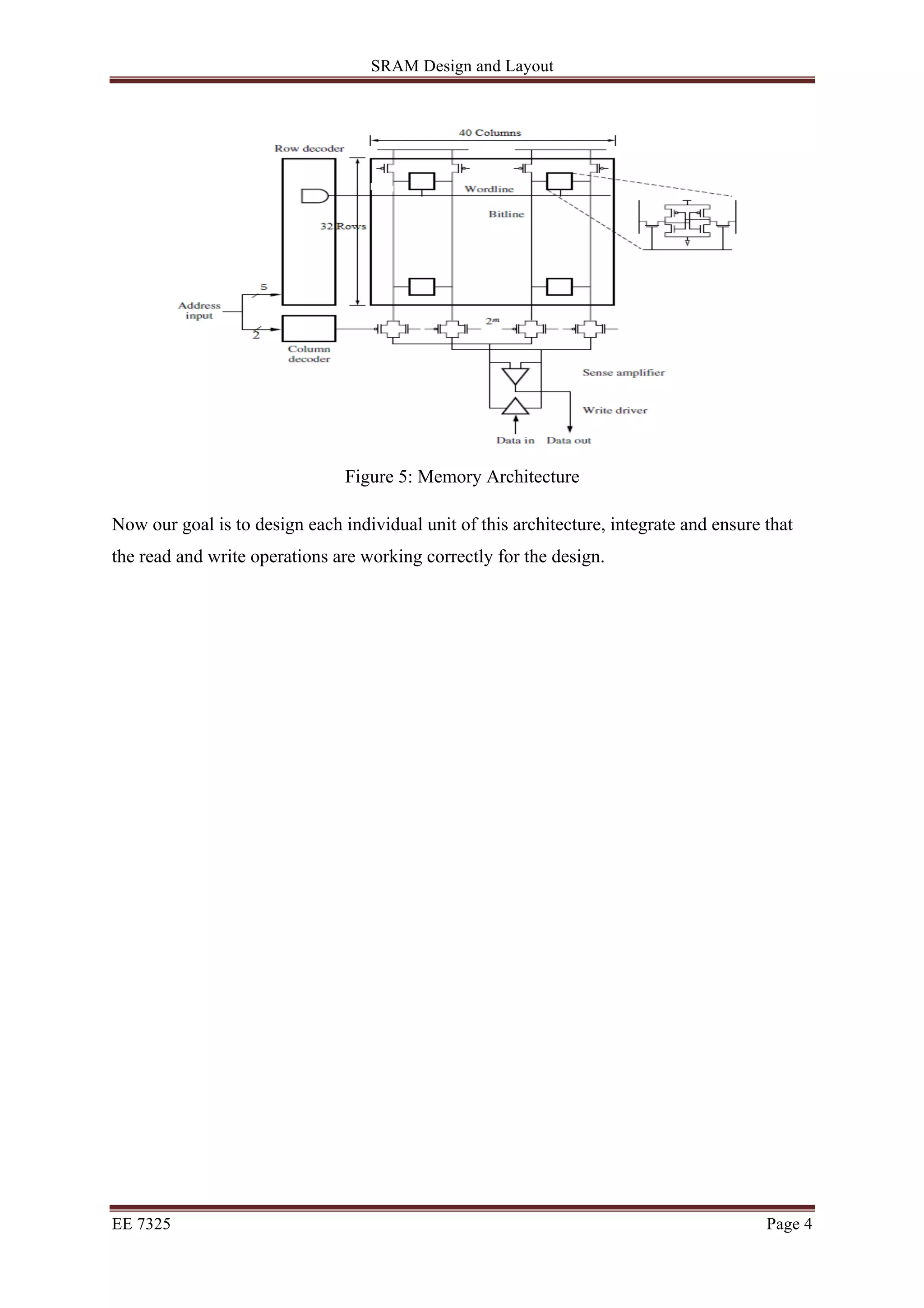
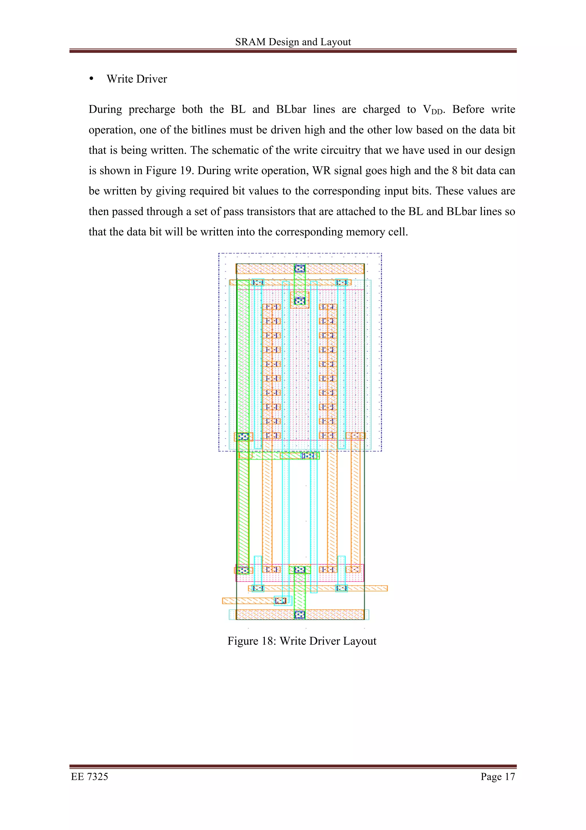
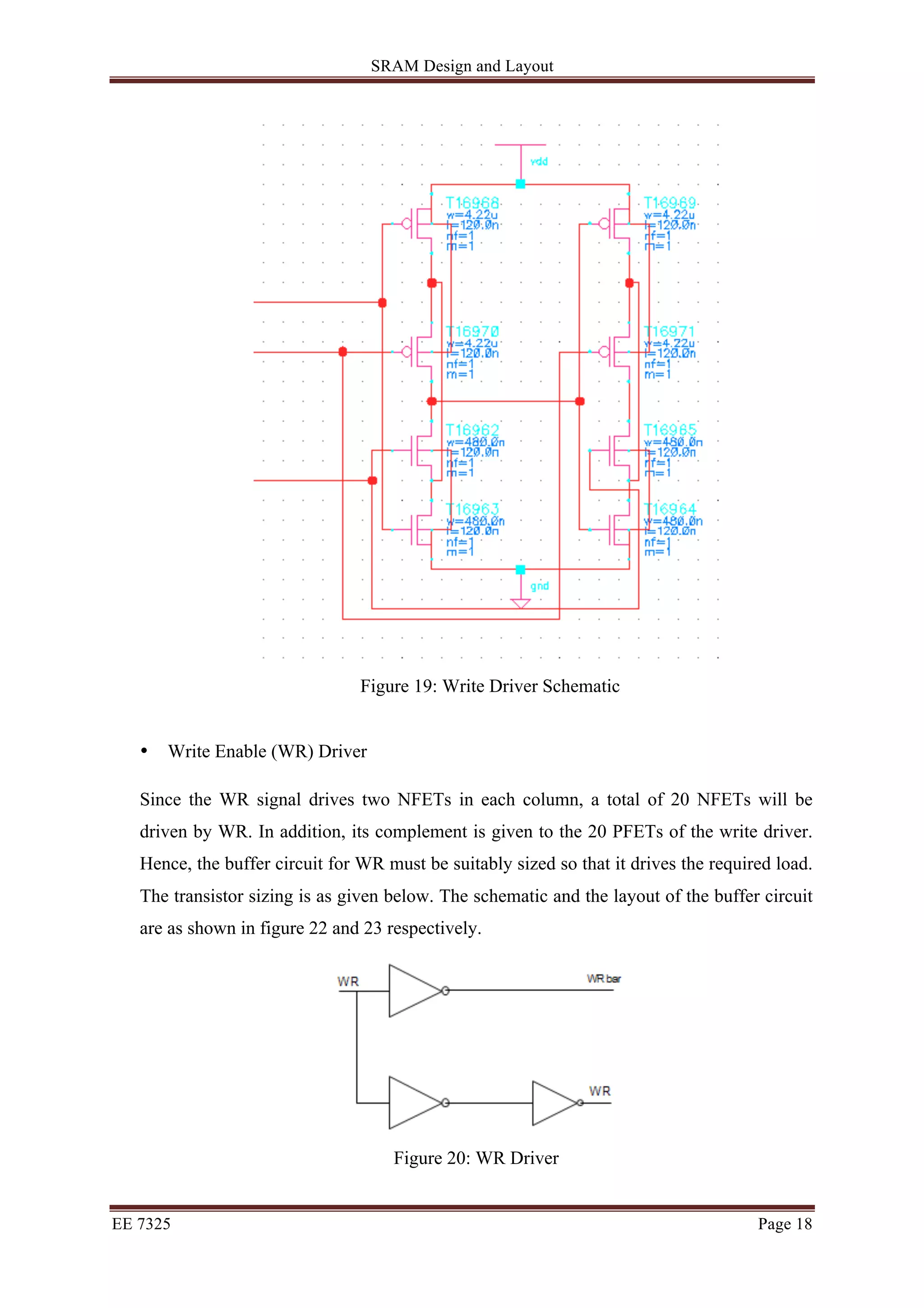
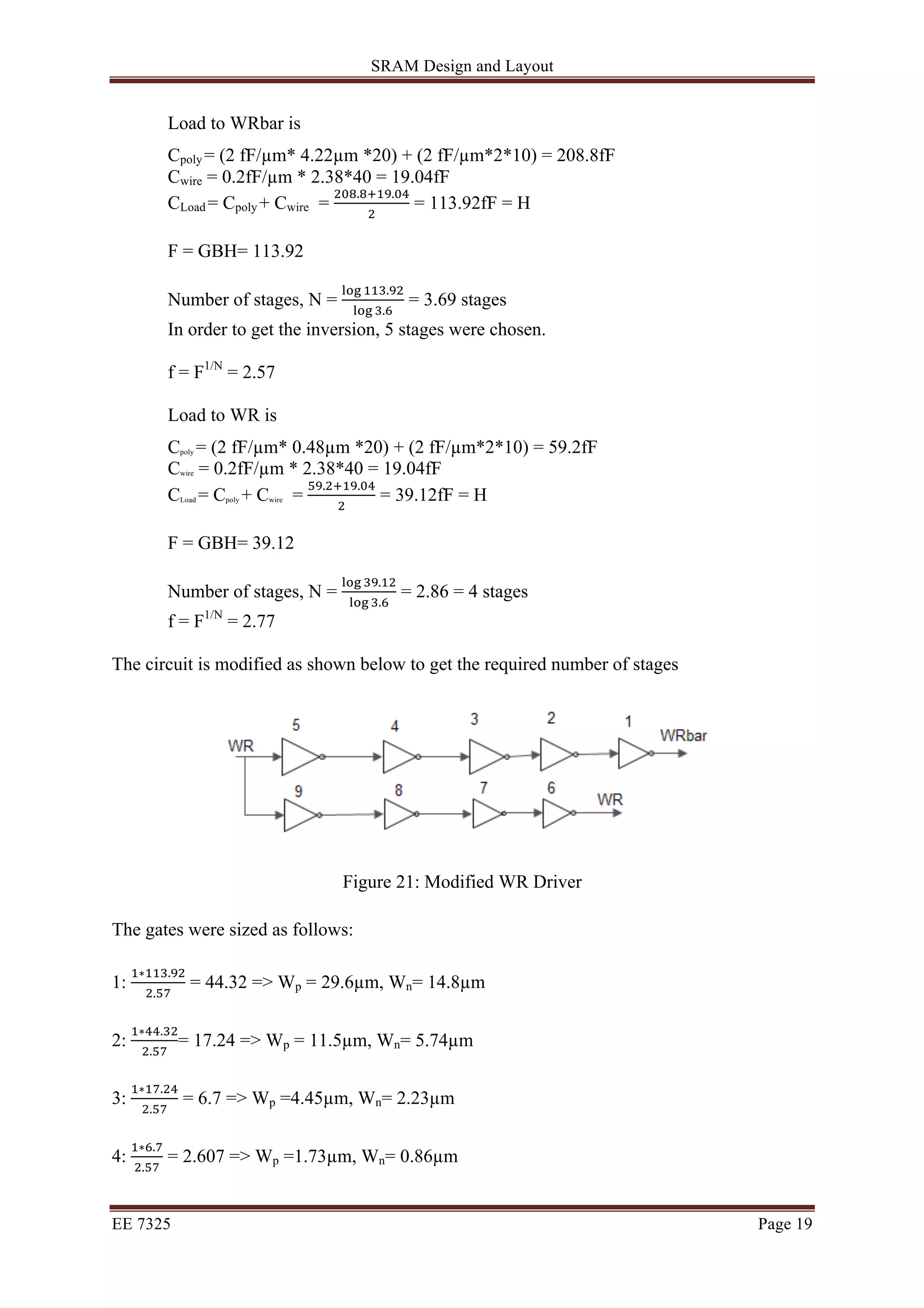
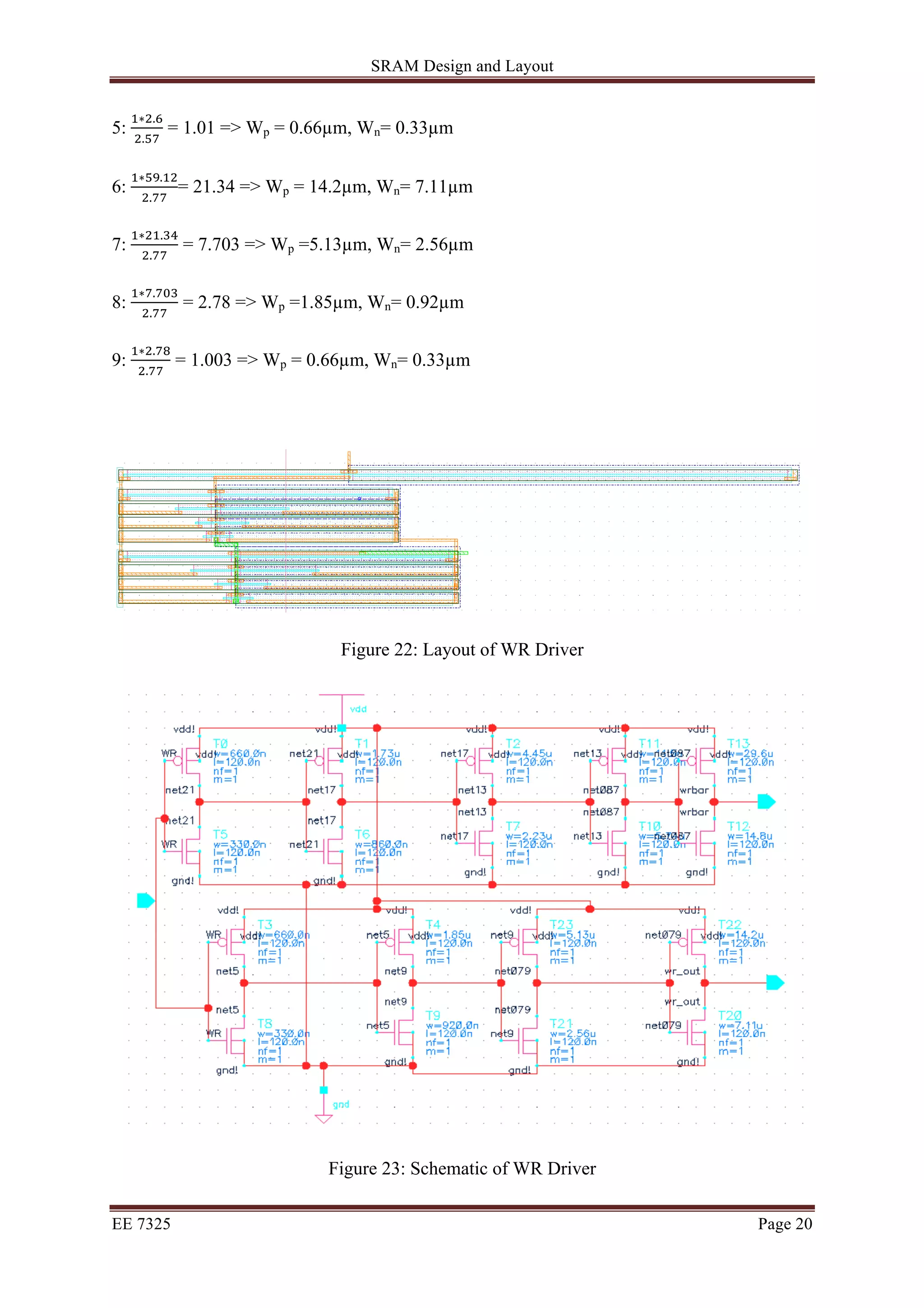

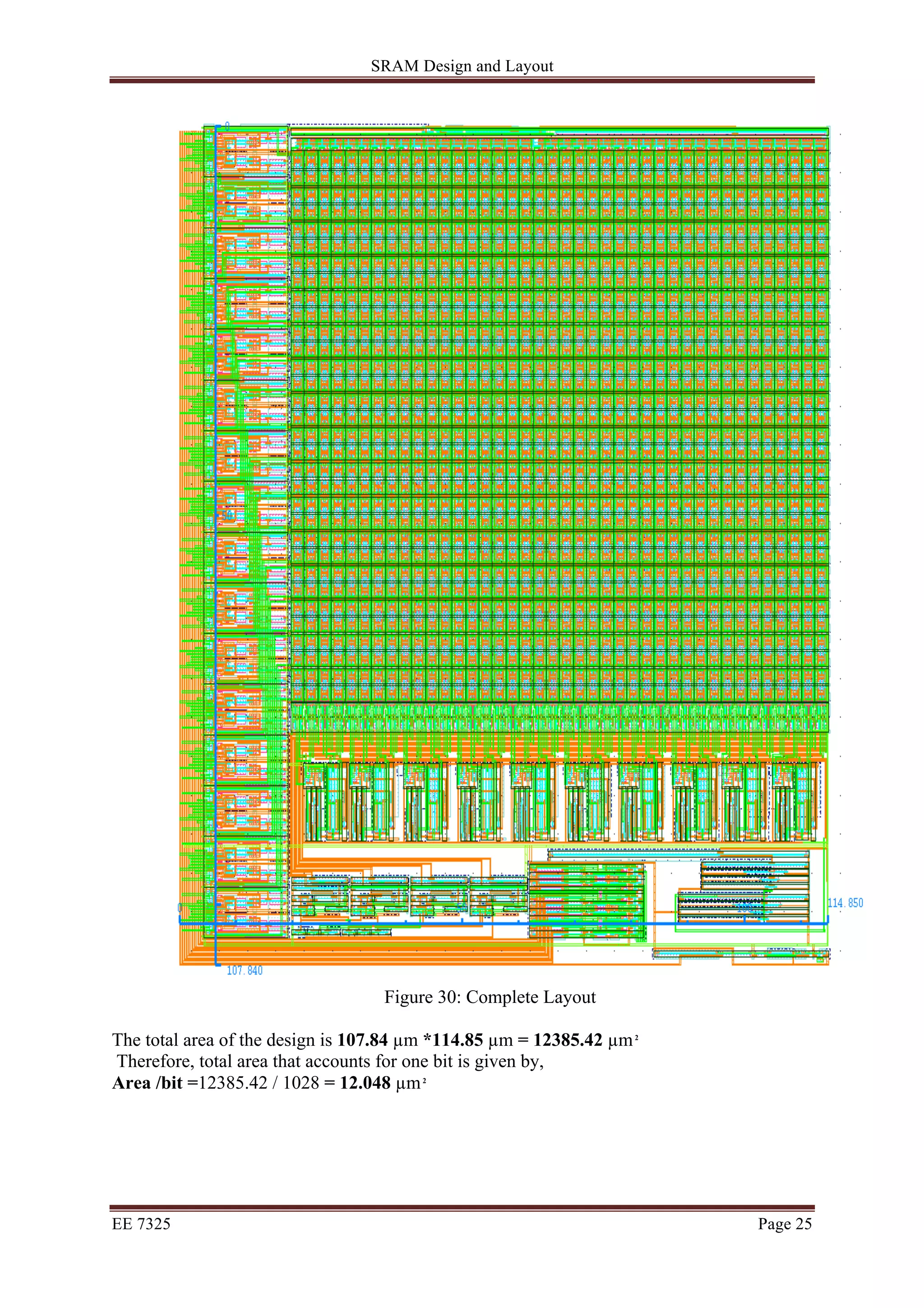

The document outlines the design and layout of a 128-word SRAM using the IBM 130nm process, focusing on key design tools and circuit components such as SRAM cells, precharge circuits, clock drivers, sense amplifiers, row and column decoders, and write drivers. It details the operational principles for reading and writing to the SRAM, employing simulations and sizing guidelines for transistors to optimize performance and minimize area requirements. The architecture consists of 1280 memory cells arranged in 40 columns and 32 rows, with various supporting circuits designed for efficient data handling.