Downloaded 389 times


![Activity factors of basic gates
• AND
• OR
• XOR
A B A B (1 p p ) p p
(1 )(1 )[1 (1 )(1 )] A B A B p p p p
[1 ( 2 )]( 2 ) A B A B A B A B p p p p p p p p](https://image.slidesharecdn.com/powerdissipationcmos-140820084027-phpapp01/85/Power-dissipation-cmos-6-320.jpg)
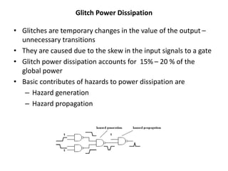


This document discusses power dissipation in CMOS circuits. It identifies the main sources of power dissipation as dynamic, static, and short circuit power. Dynamic power is caused by charging and discharging capacitors during switching and depends on activity factors, voltage, and frequency. Static power includes leakage currents that occur even when the device is inactive. Short circuit power arises when both NMOS and PMOS are on simultaneously during signal transitions. The document provides techniques for reducing each type of power dissipation such as lowering voltage, reducing switching activity, minimizing capacitance and transistor sizing.