IJERD (www.ijerd.com) International Journal of Engineering Research and Development hard copy of journal, Call for Papers 2012, publishing of journal, journal of science and technology, research paper publishing, where to publish research paper, journal
The document summarizes a research paper that proposes a new 8T SRAM cell design to improve read stability and reduce leakage current in 45nm technology compared to a conventional 6T SRAM cell. The proposed 8T cell uses a dynamic column-based power supply to raise the supply voltage during read operations, improving read stability. Simulation results using Cadence tools show the 8T cell achieves better read stability and lower leakage than the 6T cell in 45nm technology. The document provides details on stability analysis using N-curves, the operation of the conventional 6T cell, the construction and operation of the proposed 8T cell, and the simulation methodology.
CELL STABILITY ANALYSIS OF CONVENTIONAL 6T DYNAMIC 8T SRAM CELL IN 45NM TECHN...VLSICS Design
A SRAM cell must meet requirements for operation in submicron/nano ranges. The scaling of CMOS technology has significant impact on SRAM cell -- random fluctuation of electrical characteristics and substantial leakage current. In this paper we present dynamic column based power supply 8T SRAM cell and comparing the proposed SRAM cell with respect to conventional SRAM 6T in various aspects. To verify read stability and write ability analysis we use N-curve metric. Simulation results affirmed that proposed 8T SRAM cell achieved improved read stability, read current, and leakage current in 45nm Technology comparing with conventional 6T SRAM using cadence virtuoso tool.
IOSR journal of VLSI and Signal Processing (IOSRJVSP) is an open access journal that publishes articles which contribute new results in all areas of VLSI Design & Signal Processing. The goal of this journal is to bring together researchers and practitioners from academia and industry to focus on advanced VLSI Design & Signal Processing concepts and establishing new collaborations in these areas.
IJERA (International journal of Engineering Research and Applications) is International online, ... peer reviewed journal. For more detail or submit your article, please visit www.ijera.com
Energy optimization of 6T SRAM cell using low-voltage and high-performance in...IJECEIAES
The performance of the cell deteriorates, when static random access memory (SRAM) cell is operated below 1V supply voltage with continuous scale down of the complementary metal oxide semiconductor (CMOS) technology. The conventional 6T, 8T-SRAM cells suffer writeability and read static noise margins (SNM) at low-voltages leads to degradation of cell stability. To improve the cell stability and reduce the dynamic power dissipation at low- voltages of the SRAM cell, we proposed four SRAM cells based on inverter structures with less energy consumption using voltage divider bias current sink/source inverter and NOR/NAND gate using a pseudo-nMOS inverter. The design and implementation of SRAM cell using proposed inverter structures are compared with standard 6T, 8T and ST-11T SRAM cells for different supply voltages at 22-nm CMOS technology exhibit better performance of the cell. The read/write static noise margin of the cell significantly increases due to voltage divider bias network built with larger cell-ratio during read path. The load capacitance of the cell is reduced with minimized switching transitions of the devices during high-to-low and low- to-high of the pull-up and pull-down networks from VDD to ground leads to on an average 54% of dynamic power consumption. When compared with the existing ones, the read/write power of the proposed cells is reduced to 30%. The static power gets reduced by 24% due to stacking of transistors takes place in the proposed SRAM cells as compare to existing ones. The layout of the proposed cells is drawn at a 45-nm technology, and occupies an area of 1.5 times greater and 1.8 times greater as compared with 6T-SRAM cell.
SINGLE-PORT FIVE-TRANSISTOR SRAM CELL WITH REDUCED LEAKAGE CURRENT IN STANDBYVLSICS Design
In this paper, a new single-port five-transistor (5T) Static Random Access Memory (SRAM) cell with
integrated read/write assist is proposed. Amongst the assist circuitry, a voltage control circuit is coupled to
the sources corresponding to driver transistors of each row memory cells. This configuration is aimed to
control the source voltages of driver transistors under different operating modes. Specifically, during a
write operation, by means of sizing the driver transistor close to bitline to resolve the write ‘1’ issue. In
addition, associated with a two-stage reading mechanism to increase the reading speed and to avoid
unnecessary power consumption. Finally, with the standby start-up cir
IJERA (International journal of Engineering Research and Applications) is International online, ... peer reviewed journal. For more detail or submit your article, please visit www.ijera.com
FIVE-TRANSISTOR SINGLE-PORT SRAM BIT CELL WITH HIGH SPEED AND LOW STANDBY CUR...VLSICS Design
In this paper, a new five-transistor (5T) single-port Static Random Access Memory (SRAM) cell with voltage assist is proposed. Amongst them, a word line suppression circuit is designed to provide a voltage of the respective connected word line signal in a selected row cells lower than the power supply voltage VDD by a threshold voltage during a read operation, thereby to improve the read/write-ability of the cell. In addition, a voltage control circuit is coupled to the sources corresponding to driver transistors of each row memory cells. This configuration is aimed to control the source voltages of driver transistors under different operating modes. Specifically, during a read operation, a two-stage reading mechanism is engaged to increase the reading speed. Simulation results for the proposed cell design confirm that there is a conspicuous improvement in reading speed and power saving over the conventional SRAM cells, and fast writing also can be achieved.
Design of a 64-bit ultra low latency memory using 6T SRAM cells and PDK 45nm technology on CADENCE to simulate the results of our chosen implementation.
A SINGLE-ENDED AND BIT-INTERLEAVING 7T SRAM CELL IN SUB-THRESHOLD REGION WITH...jedt_journal
In recent years, to reduce power consumption and increase cell resistance against soft error, several subthreshold SRAM cell have been provided. Also, in the memory design, to increase the memory density and reduce the occupied area, sub-100 nm technologies have been used. These technologies also increase the sensitivity of the cell against soft error. Among the proposed methods to confront soft error, bitinterleaving
structure is one of the most successful methods. But the designed bit-interleaving cells usually have many transistors in order to achieve the ideal features. Moreover, another problem in the bitinterleaving cells is half-select issue. In this paper, a single-ended sub-threshold cell is presented. This cell has been designed in multi-Vt 32nm technology. On the other hand, the suggested cell can be implemented in the bit-interleaving structure to confront soft error. In the cell, 7 transistors have been used while the cell is without half-select problem. Simulations show the suggested cell has less power consumption compared with standard 6T and other bit-interleaving cells. Also, in the proposed cell, write margin and
write time delay are better than the under comparison cells, while the suggested cell stability in read and hold modes and read time delay are also optimal.
FPGA IMPLEMENTATION OF LOW POWER SRAM BASED PROCESSOR IN 8T USING HETTSEditor IJMTER
In MOSFETs lower limit sub threshold swing (60mv/decade) restricts the low power
operation. Low voltage operation is enabled by low Vth while maintaining performance. Hence steep
sub threshold slopes provide power-efficient operation without any loss of performance. To obtain
sub threshold swings of less than 30mV/decade with large ON current, Si/SiGe heterojunction
tunneling transistor uses gate controlled modulation. To overcome the impact of HETT
characteristics on SRAM, seven transistors HETT based SRAM design is introduced. Compared to
CMOS this new 8T HETT SRAM achieves reduction in leakage power.
Design of Low Voltage D-Flip Flop Using MOS Current Mode Logic (MCML) For Hig...IOSRJVSP
This paper presents a new topology to implement MOS current mod logic (MCML) tri-state buffers. In Mos current mode logic (MCML) current section is improves the performance and maintains low power of the circuit. MCML circuits contains true differential operation by which provides the feature of low noise level generation and static power dissipation. So the amount of current drawn from the power supply does not depends on the switching activity. Due to this MOS current mode logic (MCML) circuits have been useful for developing analog and mixed signal IC’s. The implementing of MCML D-flip flop and Frequency divider done by using MCML D-latches. The proposed MCML D-latch consumes less power as it makes use of low power tri-state buffers. Which promotes power saving due to reduction in the overall current flow in the proposed D flip flop topology is verified though Cadence GPDK-180nM CMOS technology parameters.
A Design Technique To Reduce Nbti Effects From 5t Sram CellsIJERA Editor
This paper focuses on designing an NBTI tolerant system by addressing the major reason of NBTI especially the devices that consists of SOC. To address this issue a thorough study of 5T SRAM cells has been done. This paper is based on idea of switch capacitors and the fact that only few transistors are ON at any particular time. RD model is primary and base model that us used to describe NBTI and aging degradation in this paper The proposed technique improve read power by 8% and leakage power by 12.87%
IJRET : International Journal of Research in Engineering and Technology is an international peer reviewed, online journal published by eSAT Publishing House for the enhancement of research in various disciplines of Engineering and Technology. The aim and scope of the journal is to provide an academic medium and an important reference for the advancement and dissemination of research results that support high-level learning, teaching and research in the fields of Engineering and Technology. We bring together Scientists, Academician, Field Engineers, Scholars and Students of related fields of Engineering and Technology
A Simplied Bit-Line Technique for Memory Optimizationijsrd.com
High fan-in and fan-out in read-write of memory requires more area, power, and causes large propagation delay .The number of transistor counts also increases due to large fan-in and fan-out. A simplified bit line technique for power optimization of memory proposed consumes steady power, requires less number of transistors and hence reduces the propagation delay for any fan-in and fan-out of read-write memory. Adopting simplified bit line technique, we implemented 32-word 16-bits/word, 32-word 16-bits/word and so on, 1-read, 1-write ported register files in a 1.2-V/2.5V. By using this technique 2n word x m-bits/words can be achieved with steady power consumption of 2.4mW for 1.2V/2.5V, this power consumption can be further reduced to half of present level by constraining the parameters such as temperature, speed, frequency of operation etc for processing technology.
International Journal of Engineering Research and Development (IJERD)IJERD Editor
journal publishing, how to publish research paper, Call For research paper, international journal, publishing a paper, IJERD, journal of science and technology, how to get a research paper published, publishing a paper, publishing of journal, publishing of research paper, reserach and review articles, IJERD Journal, How to publish your research paper, publish research paper, open access engineering journal, Engineering journal, Mathemetics journal, Physics journal, Chemistry journal, Computer Engineering, Computer Science journal, how to submit your paper, peer reviw journal, indexed journal, reserach and review articles, engineering journal, www.ijerd.com, research journals,
yahoo journals, bing journals, International Journal of Engineering Research and Development, google journals, hard copy of journal
A Single-Ended With Dynamic Feedback Control 8T Subthreshold SRAM Cell Ieee Xpert
A Single-Ended With Dynamic Feedback Control
8T Subthreshold SRAM Cell
A Single-Ended With Dynamic Feedback Control
8T Subthreshold SRAM Cell
A Single-Ended With Dynamic Feedback Control
8T Subthreshold SRAM Cell
A Single-Ended With Dynamic Feedback Control
8T Subthreshold SRAM Cell
A Single-Ended With Dynamic Feedback Control
8T Subthreshold SRAM Cell
This paper presents a spin-transfer torque- magnetic
tunnel junction (STT-MTJ) based non-volatile 9-transistor
(9T) SRAM cell. The cell achieves low power dissipation due
to its series connected MTJ elements and read buffer which
offer stacking effect. The paper studies the impact of PVT
(process, voltage, and temperature) variations on the design
metric of the SRAM cell such as write delay and compares the
results with non-volatile 8T SRAM cell (NV8T). The proposed
design consumes lower leakage power and exhibits narrower
spread in write delay compared with NV8T.
VLSI stands for Very Large Scale Integration. Generally there are mainly 2 types of VLSI projects – 1. Projects in VLSI based System Design, 2. VLSI Design Projects. You might be confused to understand the difference between these 2 types of projects. Let me now explain to you.
Projects in VLSI based system design are the projects which involve the design of various types of digital systems that can be implemented on a PLD device like a FPGA or a CPLD.
IJRET : International Journal of Research in Engineering and Technology is an international peer reviewed, online journal published by eSAT Publishing House for the enhancement of research in various disciplines of Engineering and Technology. The aim and scope of the journal is to provide an academic medium and an important reference for the advancement and dissemination of research results that support high-level learning, teaching and research in the fields of Engineering and Technology. We bring together Scientists, Academician, Field Engineers, Scholars and Students of related fields of Engineering and Technology.
Designed a fully customized 128x10b SRAM by constructing schematic & virtuoso layout of memory cell array (6T cell), row & column decoder, pre-charge circuit, write circuit and sense amplifier using Cadence. Manually placed and routed all components, performed DRC & LVS debugging of constructed schematic and layout and ran PEX to generate the final Netlist, Hspice Spectre simulation of final design for verification of the correct functionality and analysis of best read, best write cycles & the worst case timing for read and write. Timing and power consumed is analyzed through STA-Primetime (Static timing Analysis)
Similar to IJERD (www.ijerd.com) International Journal of Engineering Research and Development hard copy of journal, Call for Papers 2012, publishing of journal, journal of science and technology, research paper publishing, where to publish research paper, journal
Implementation of High Reliable 6T SRAM Cell Designiosrjce
Memory can be formed with the integration of large number of basic storing element called cells.
SRAM cell is one of the basic storing unit of volatile semiconductor memory that stores binary logic '1' or '0' bit.
Modified read and write circuits were proposed in this paper to address incorrect read and write operations in
conventional 6T SRAM cell design available in open literature. Design of a new highly reliable 6T SRAM cell
design is proposed with reliable read, write operations and negative bit line voltage (NBLV). Simulations are
carried out using MENTOR GRAPHICS
250nm Technology Based Low Power SRAM Memoryiosrjce
High integration density, low power and fastperformance are all critical parameters in designing of
memory blocks. Static Random Access Memories (SRAMs)’s focusing on optimizing dynamic power concept of
virtual source transistors is used for removing direct connection between VDD and GND.
Also stacking effect can be reduced by switching off the stacktransistors when the memory is ideal and the
leakage current using SVL techniques This paper discusses the evolution of 9t SRAM circuits in terms of low
power consumption, The whole circuit verification is done on the Tanner tool, Schematic of the
SRAM cell is designed on the S-Edit and net list simulation done by using T-spice and waveforms are analyzed
through the W-edit
Static-Noise-Margin Analysis of Modified 6T SRAM Cell during Read Operationidescitation
As modern technology is spreading fast, it is very
important to design low power, high performance, fast
responding SRAM(Static Random Access Memory) since they
are critical component in high performance processors. In
this paper we discuss about the noise effect of different SRAM
circuits during read operation which hinders the stability of
the SRAM cell. This paper also represents a modified 6T
SRAM cell which increases the cell stability without
increasing transistor count.
IMPLEMENTATION OF LOW POWER ADIABATIC SRAMVLSICS Design
In the featuring VLSI era, compact electronic devices are popular. The reliability and durability of such compact devices relies on low power utilization. The purpose of this project was to implement a low power adiabatic Static Random Access Memory (SRAM), with the following objectives - To reduce the power waste by means of stepwise charging using tank capacitors which is an adiabatic way of generating power clock. This method is capable of recuperating the electrical energy back to the source. Further to examine the Static Noise Margin (SNM) – a parameter which gives detailed information about the cell stability – in contrast with conventional 6T, 7T and 8T topologies of SRAM under 180 nm technology. Finally, SNM variations with respect to process parameters are also discussed. All the implementations and analysis were made using CADENCE tool and MATLAB tool.
IMPLEMENTATION OF LOW POWER ADIABATIC SRAMVLSICS Design
In the featuring VLSI era, compact electronic devices are popular. The reliability and durability of such compact devices relies on low power utilization. The purpose of this project was to implement a low power adiabatic Static Random Access Memory (SRAM), with the following objectives - To reduce the power waste by means of stepwise charging using tank capacitors which is an adiabatic way of generating power
clock. This method is capable of recuperating the electrical energy back to the source. Further to examine the Static Noise Margin (SNM) – a parameter which gives detailed information about the cell stability – in
contrast with conventional 6T, 7T and 8T topologies of SRAM under 180 nm technology. Finally, SNM variations with respect to process parameters are also discussed. All the implementations and analysis were made using CADENCE tool and MATLAB tool.
IMPLEMENTATION OF LOW POWER ADIABATIC SRAMVLSICS Design
In the featuring VLSI era, compact electronic devices are popular. The reliability and durability of such compact devices relies on low power utilization. The purpose of this project was to implement a low power adiabatic Static Random Access Memory (SRAM), with the following objectives - To reduce the power waste by means of stepwise charging using tank capacitors which is an adiabatic way of generating power
clock. This method is capable of recuperating the electrical energy back to the source. Further to examine the Static Noise Margin (SNM) – a parameter which gives detailed information about the cell stability – in contrast with conventional 6T, 7T and 8T topologies of SRAM under 180 nm technology. Finally, SNM
variations with respect to process parameters are also discussed. All the implementations and analysis were made using CADENCE tool and MATLAB tool.
Design & Implementation of Subthreshold Memory Cell design based on the prima...IOSRJVSP
As there is a demand for portable electronic systems or devices, there is an incremental growth in the technology in the past few decades and also technology is cumulative at a random rate, devices are consuming large amount of power due to this the life of the battery is draining fast. so there must be a alternative devices or circuits which can reduce the power by efficiently maintaining the area and performance, therefore life of battery can be increased. As SRAM is the heart of block in all the electronic design, where the power consumption is maximum there by analyzing, estimating & modifying or changing the logic, will be able to reduce the power and performance can be greatly achieved. This proposal describes under the principle of ultra-low power logic approach which operates under subthreshold voltage operating which leads to lower power and also efficient in functionality along with secondary constraints.
IOSR Journal of Electronics and Communication Engineering(IOSR-JECE) is an open access international journal that provides rapid publication (within a month) of articles in all areas of electronics and communication engineering and its applications. The journal welcomes publications of high quality papers on theoretical developments and practical applications in electronics and communication engineering. Original research papers, state-of-the-art reviews, and high quality technical notes are invited for publications.
IJERA (International journal of Engineering Research and Applications) is International online, ... peer reviewed journal. For more detail or submit your article, please visit www.ijera.com
A Novel Low Power Energy Efficient SRAM Cell With Reduced Power Consumption u...iosrjce
In modern high performance integrated circuits, maximum of the total active mode energy is
consumed due to leakage current. SRAM cell array is main source of leakage current since majority of
transistor are utilized for on-chip memory in today high performance microprocessor and system on chip
designs. Therefore the design of low leakage SRAM is required. Reducing power dissipation, supply voltage,
leakage currents, area of chip are the most important parameters in today`s VLSI designs. But scaling of these
parameters will lead to drastic increase in sub threshold leakage currents and power dissipation because of that
performance of the design is degraded. So to overcome these issues it is better to concentrate on reduction of
active leakage currents and dynamic power dissipation by using power reduction techniques. In this paper 9T
SRAM (data retention p-gated) cell for low voltage and energy constrain application is analyzed with respect to
power dissipation, area and delay. The analyzed design of 9T SRAM cell with MTCMOS technique has been
proposed. Designed circuits are simulated in Microwind 3.1 VLSI CAD Tool in 90 and 65nm CMOS technology.
Average and Static Power Analysis of a 6T and 7T SRAM Bit-Cell at 180nm, 90nm...idescitation
A lot of consideration has been given to problems arising due to power dissipation.
Different ideas have been proposed by many researchers from the device level to the
architectural level and above. However, there is no universal way to avoid tradeoffs between
the power, delay and area. This is why; the designers are required to choose appropriate
techniques that satisfy application and product needs. Another important component of
power which contributes to power dissipation is Dynamic Power. This power is increasing
due to prolonged use of the electronic equipments. This is due to the fact that now-a-days
people are working on electronic systems from morning till night; it may be a mobile phone
or a laptop or any other equipment. This paper deals with the estimation of two components
of power i.e. static power (when device is in the standby mode) and the average power
(average amount of energy consumed with respect to time) of a 6T and 7T SRAM (Static
Random Access Memory) bit-cell at 180nm, 90nm, and 45nm CMOS Technology. This is
done in order to estimate the power required for a high speed operation of 6T and 7T
SRAM bit-cell.
A Comparitive Analysis of Improved 6t Sram Cell With Different Sram CellIJERA Editor
High speed and low power consumption have been the primary issue to design Static Random Access Memory (SRAM), but we are facing new challenges with the scaling of technology. The stability and speed of SRAM are important issues to improve efficiency and performance of the system. Stability of the SRAM depends on the static noise margin (SNM) so the noise margin is also important parameter for the design of memory because the higher noise margin confirms the high speed of the SRAM cell. In this paper, the improved 6T SRAM cell shows maximum reduction in power consumption of 88%, maximum reduction in delay of 64% and maximum SNM of 17% increases compared with 7T SRAM cell.
“Power and Temperature Analysis of 12T CMOS SRAM Designed With Short Channel ...iosrjce
This paper focuses mainly on dynamic power dissipations at different temperature for both read and
write operations of 12T SRAM. In the proposed 12T structure virtual vdd concept is employed because of this
leakage current will reduce. Hence reduction in leakage current causes reduction in dynamic power. Power
dissipation of the proposed SRAM cell have been determined and compared to those of some other existing
memory cells. Proposed cell is a short channel BSIM4 model. It is observed that power dissipation of 12T
SRAM for read operation at 40̊
̊
is 44.7nw and for write operation it is 38.79nw. The proposed SRAM cell
dissipates less power. Simulation has been done in Tanner-13 EDA tool for 50nm.
Large number of interconnection
requirement has become a major limitation to the designs
using binary logic. One of the solutions for this is MultipleValued
Logic (MVL). MVL proves to be advantageous as it
reduces dynamic power dissipation, increases computational
ability, data density and requires less number of
interconnects. In this paper, the implementation of a Static
Random Access Memory (SRAM) cell using a quaternary D
Latch is proposed. The D Latch is built using NMAX, NMIN
and quaternary inverter circuit. Using this SRAM cell a 4X4
SRAM array is constructed and is compared with 4X4 array
of Quaternary Static CMOS memory cell. The spice coding
is done using 0.18μm CMOS technology and verification of
the design is done through HSPICE and COSMOSSCOPE
Synopsis Tools. Power and delay of the circuit is analyzed.
Implementation of an Efficient SRAM for Ultra-Low Voltage Application Based o...IOSR Journals
Abstract: Operation of standard 6T static random access memory (SRAM) cells at sub or near threshold
voltages is unfeasible, predominantly due to degraded static noise margins (SNM) and poor robustness. We
analyze Schmitt-Trigger (ST)-based differential-sensing static random access memory (SRAM) bitcells for
ultralow-voltage operation. The ST-based SRAM bitcells address the fundamental conflicting design
requirement of the read versus write operation of a conventional 6T bitcell. The ST operation gives better readstability
as well as better write-ability compared to the standard 6T bitcell. In this paper we are going to
propose a new SRAM bitcell for the purpose of read stability and write ability by using 90nm technology , and
less power consumption, less area than the existing Schmitt trigger1 based SRAM. Design and simulations were done using DSCH and Microwind.
Index Terms: read stability, write ability, Schmitt trigger.
PERFORMANCE EVALUATION OF DIFFERENT SRAM CELL STRUCTURES AT DIFFERENT TECHNOL...VLSICS Design
In recent years the demand for low power devices has been increases tremendously. To solve the power dissipation problem, many researchers have proposed different ideas from the device level to the architectural level and above. However, there is no universal way to avoid tradeoffs between power, delay and area, thus designers are required to choose appropriate techniques that satisfy application and product needs. The demand for static random-access memory (SRAM) is increasing with large use of SRAM in System On-Chip and high-performance VLSI circuits. This paper represents the simulation of different SRAM cells and their comparative analysis on different parameters such as Power Supply Voltage, area efficiency etc to enhance the performance. All the simulations have been carried out on BSIM 3V3 90nm, 45nm and 32 technology at Tanner EDA tool.
Similar to IJERD (www.ijerd.com) International Journal of Engineering Research and Development hard copy of journal, Call for Papers 2012, publishing of journal, journal of science and technology, research paper publishing, where to publish research paper, journal (20)
A Novel Method for Prevention of Bandwidth Distributed Denial of Service AttacksIJERD Editor
Distributed Denial of Service (DDoS) Attacks became a massive threat to the Internet. Traditional
Architecture of internet is vulnerable to the attacks like DDoS. Attacker primarily acquire his army of Zombies,
then that army will be instructed by the Attacker that when to start an attack and on whom the attack should be
done. In this paper, different techniques which are used to perform DDoS Attacks, Tools that were used to
perform Attacks and Countermeasures in order to detect the attackers and eliminate the Bandwidth Distributed
Denial of Service attacks (B-DDoS) are reviewed. DDoS Attacks were done by using various Flooding
techniques which are used in DDoS attack.
The main purpose of this paper is to design an architecture which can reduce the Bandwidth
Distributed Denial of service Attack and make the victim site or server available for the normal users by
eliminating the zombie machines. Our Primary focus of this paper is to dispute how normal machines are
turning into zombies (Bots), how attack is been initiated, DDoS attack procedure and how an organization can
save their server from being a DDoS victim. In order to present this we implemented a simulated environment
with Cisco switches, Routers, Firewall, some virtual machines and some Attack tools to display a real DDoS
attack. By using Time scheduling, Resource Limiting, System log, Access Control List and some Modular
policy Framework we stopped the attack and identified the Attacker (Bot) machines
Hearing loss is one of the most common human impairments. It is estimated that by year 2015 more
than 700 million people will suffer mild deafness. Most can be helped by hearing aid devices depending on the
severity of their hearing loss. This paper describes the implementation and characterization details of a dual
channel transmitter front end (TFE) for digital hearing aid (DHA) applications that use novel micro
electromechanical- systems (MEMS) audio transducers and ultra-low power-scalable analog-to-digital
converters (ADCs), which enable a very-low form factor, energy-efficient implementation for next-generation
DHA. The contribution of the design is the implementation of the dual channel MEMS microphones and powerscalable
ADC system.
Influence of tensile behaviour of slab on the structural Behaviour of shear c...IJERD Editor
-A composite beam is composed of a steel beam and a slab connected by means of shear connectors
like studs installed on the top flange of the steel beam to form a structure behaving monolithically. This study
analyzes the effects of the tensile behavior of the slab on the structural behavior of the shear connection like slip
stiffness and maximum shear force in composite beams subjected to hogging moment. The results show that the
shear studs located in the crack-concentration zones due to large hogging moments sustain significantly smaller
shear force and slip stiffness than the other zones. Moreover, the reduction of the slip stiffness in the shear
connection appears also to be closely related to the change in the tensile strain of rebar according to the increase
of the load. Further experimental and analytical studies shall be conducted considering variables such as the
reinforcement ratio and the arrangement of shear connectors to achieve efficient design of the shear connection
in composite beams subjected to hogging moment.
Gold prospecting using Remote Sensing ‘A case study of Sudan’IJERD Editor
Gold has been extracted from northeast Africa for more than 5000 years, and this may be the first
place where the metal was extracted. The Arabian-Nubian Shield (ANS) is an exposure of Precambrian
crystalline rocks on the flanks of the Red Sea. The crystalline rocks are mostly Neoproterozoic in age. ANS
includes the nations of Israel, Jordan. Egypt, Saudi Arabia, Sudan, Eritrea, Ethiopia, Yemen, and Somalia.
Arabian Nubian Shield Consists of juvenile continental crest that formed between 900 550 Ma, when intra
oceanic arc welded together along ophiolite decorated arc. Primary Au mineralization probably developed in
association with the growth of intra oceanic arc and evolution of back arc. Multiple episodes of deformation
have obscured the primary metallogenic setting, but at least some of the deposits preserve evidence that they
originate as sea floor massive sulphide deposits.
The Red Sea Hills Region is a vast span of rugged, harsh and inhospitable sector of the Earth with
inimical moon-like terrain, nevertheless since ancient times it is famed to be an abode of gold and was a major
source of wealth for the Pharaohs of ancient Egypt. The Pharaohs old workings have been periodically
rediscovered through time. Recent endeavours by the Geological Research Authority of Sudan led to the
discovery of a score of occurrences with gold and massive sulphide mineralizations. In the nineties of the
previous century the Geological Research Authority of Sudan (GRAS) in cooperation with BRGM utilized
satellite data of Landsat TM using spectral ratio technique to map possible mineralized zones in the Red Sea
Hills of Sudan. The outcome of the study mapped a gossan type gold mineralization. Band ratio technique was
applied to Arbaat area and a signature of alteration zone was detected. The alteration zones are commonly
associated with mineralization. The alteration zones are commonly associated with mineralization. A filed check
confirmed the existence of stock work of gold bearing quartz in the alteration zone. Another type of gold
mineralization that was discovered using remote sensing is the gold associated with metachert in the Atmur
Desert.
Reducing Corrosion Rate by Welding DesignIJERD Editor
The paper addresses the importance of welding design to prevent corrosion at steel. Welding is
used to join pipe, profiles at bridges, spindle, and a lot more part of engineering construction. The
problems happened associated with welding are common issues in these fields, especially corrosion.
Corrosion can be reduced with many methods, they are painting, controlling humidity, and also good
welding design. In the research, it can be found that reducing residual stress on the welding can be
solved in corrosion rate reduction problem.
Preheating on 500oC and 600oC give better condition to reduce corosion rate than condition after
preheating 400oC. For all welding groove type, material with 500oC and 600oC preheating after 14 days
corrosion test is 0,5%-0,69% lost. Material with 400oC preheating after 14 days corrosion test is 0,57%-0,76%
lost.
Welding groove also influence corrosion rate. X and V type welding groove give better condition to reduce
corrosion rate than use 1/2V and 1/2 X welding groove. After 14 days corrosion test, the samples with
X welding groove type is 0,5%-0,57% lost. The samples with V welding groove after 14 days corrosion test is
0,51%-0,59% lost. The samples with 1/2V and 1/2X welding groove after 14 days corrosion test is 0,58%-
0,71% lost.
Router 1X3 – RTL Design and VerificationIJERD Editor
Routing is the process of moving a packet of data from source to destination and enables messages
to pass from one computer to another and eventually reach the target machine. A router is a networking device
that forwards data packets between computer networks. It is connected to two or more data lines from different
networks (as opposed to a network switch, which connects data lines from one single network). This paper,
mainly emphasizes upon the study of router device, it‟s top level architecture, and how various sub-modules of
router i.e. Register, FIFO, FSM and Synchronizer are synthesized, and simulated and finally connected to its top
module.
Active Power Exchange in Distributed Power-Flow Controller (DPFC) At Third Ha...IJERD Editor
This paper presents a component within the flexible ac-transmission system (FACTS) family, called
distributed power-flow controller (DPFC). The DPFC is derived from the unified power-flow controller (UPFC)
with an eliminated common dc link. The DPFC has the same control capabilities as the UPFC, which comprise
the adjustment of the line impedance, the transmission angle, and the bus voltage. The active power exchange
between the shunt and series converters, which is through the common dc link in the UPFC, is now through the
transmission lines at the third-harmonic frequency. DPFC multiple small-size single-phase converters which
reduces the cost of equipment, no voltage isolation between phases, increases redundancy and there by
reliability increases. The principle and analysis of the DPFC are presented in this paper and the corresponding
simulation results that are carried out on a scaled prototype are also shown.
Mitigation of Voltage Sag/Swell with Fuzzy Control Reduced Rating DVRIJERD Editor
Power quality has been an issue that is becoming increasingly pivotal in industrial electricity
consumers point of view in recent times. Modern industries employ Sensitive power electronic equipments,
control devices and non-linear loads as part of automated processes to increase energy efficiency and
productivity. Voltage disturbances are the most common power quality problem due to this the use of a large
numbers of sophisticated and sensitive electronic equipment in industrial systems is increased. This paper
discusses the design and simulation of dynamic voltage restorer for improvement of power quality and
reduce the harmonics distortion of sensitive loads. Power quality problem is occurring at non-standard
voltage, current and frequency. Electronic devices are very sensitive loads. In power system voltage sag,
swell, flicker and harmonics are some of the problem to the sensitive load. The compensation capability
of a DVR depends primarily on the maximum voltage injection ability and the amount of stored
energy available within the restorer. This device is connected in series with the distribution feeder at
medium voltage. A fuzzy logic control is used to produce the gate pulses for control circuit of DVR and the
circuit is simulated by using MATLAB/SIMULINK software.
Study on the Fused Deposition Modelling In Additive ManufacturingIJERD Editor
Additive manufacturing process, also popularly known as 3-D printing, is a process where a product
is created in a succession of layers. It is based on a novel materials incremental manufacturing philosophy.
Unlike conventional manufacturing processes where material is removed from a given work price to derive the
final shape of a product, 3-D printing develops the product from scratch thus obviating the necessity to cut away
materials. This prevents wastage of raw materials. Commonly used raw materials for the process are ABS
plastic, PLA and nylon. Recently the use of gold, bronze and wood has also been implemented. The complexity
factor of this process is 0% as in any object of any shape and size can be manufactured.
Spyware triggering system by particular string valueIJERD Editor
This computer programme can be used for good and bad purpose in hacking or in any general
purpose. We can say it is next step for hacking techniques such as keylogger and spyware. Once in this system if
user or hacker store particular string as a input after that software continually compare typing activity of user
with that stored string and if it is match then launch spyware programme.
A Blind Steganalysis on JPEG Gray Level Image Based on Statistical Features a...IJERD Editor
This paper presents a blind steganalysis technique to effectively attack the JPEG steganographic
schemes i.e. Jsteg, F5, Outguess and DWT Based. The proposed method exploits the correlations between
block-DCTcoefficients from intra-block and inter-block relation and the statistical moments of characteristic
functions of the test image is selected as features. The features are extracted from the BDCT JPEG 2-array.
Support Vector Machine with cross-validation is implemented for the classification.The proposed scheme gives
improved outcome in attacking.
Secure Image Transmission for Cloud Storage System Using Hybrid SchemeIJERD Editor
- Data over the cloud is transferred or transmitted between servers and users. Privacy of that
data is very important as it belongs to personal information. If data get hacked by the hacker, can be
used to defame a person’s social data. Sometimes delay are held during data transmission. i.e. Mobile
communication, bandwidth is low. Hence compression algorithms are proposed for fast and efficient
transmission, encryption is used for security purposes and blurring is used by providing additional
layers of security. These algorithms are hybridized for having a robust and efficient security and
transmission over cloud storage system.
Application of Buckley-Leverett Equation in Modeling the Radius of Invasion i...IJERD Editor
A thorough review of existing literature indicates that the Buckley-Leverett equation only analyzes
waterflood practices directly without any adjustments on real reservoir scenarios. By doing so, quite a number
of errors are introduced into these analyses. Also, for most waterflood scenarios, a radial investigation is more
appropriate than a simplified linear system. This study investigates the adoption of the Buckley-Leverett
equation to estimate the radius invasion of the displacing fluid during waterflooding. The model is also adopted
for a Microbial flood and a comparative analysis is conducted for both waterflooding and microbial flooding.
Results shown from the analysis doesn’t only records a success in determining the radial distance of the leading
edge of water during the flooding process, but also gives a clearer understanding of the applicability of
microbes to enhance oil production through in-situ production of bio-products like bio surfactans, biogenic
gases, bio acids etc.
Gesture Gaming on the World Wide Web Using an Ordinary Web CameraIJERD Editor
- Gesture gaming is a method by which users having a laptop/pc/x-box play games using natural or
bodily gestures. This paper presents a way of playing free flash games on the internet using an ordinary webcam
with the help of open source technologies. Emphasis in human activity recognition is given on the pose
estimation and the consistency in the pose of the player. These are estimated with the help of an ordinary web
camera having different resolutions from VGA to 20mps. Our work involved giving a 10 second documentary to
the user on how to play a particular game using gestures and what are the various kinds of gestures that can be
performed in front of the system. The initial inputs of the RGB values for the gesture component is obtained by
instructing the user to place his component in a red box in about 10 seconds after the short documentary before
the game is finished. Later the system opens the concerned game on the internet on popular flash game sites like
miniclip, games arcade, GameStop etc and loads the game clicking at various places and brings the state to a
place where the user is to perform only gestures to start playing the game. At any point of time the user can call
off the game by hitting the esc key and the program will release all of the controls and return to the desktop. It
was noted that the results obtained using an ordinary webcam matched that of the Kinect and the users could
relive the gaming experience of the free flash games on the net. Therefore effective in game advertising could
also be achieved thus resulting in a disruptive growth to the advertising firms.
Hardware Analysis of Resonant Frequency Converter Using Isolated Circuits And...IJERD Editor
-LLC resonant frequency converter is basically a combo of series as well as parallel resonant ckt. For
LCC resonant converter it is associated with a disadvantage that, though it has two resonant frequencies, the
lower resonant frequency is in ZCS region[5]. For this application, we are not able to design the converter
working at this resonant frequency. LLC resonant converter existed for a very long time but because of
unknown characteristic of this converter it was used as a series resonant converter with basically a passive
(resistive) load. . Here, it was designed to operate in switching frequency higher than resonant frequency of the
series resonant tank of Lr and Cr converter acts very similar to Series Resonant Converter. The benefit of LLC
resonant converter is narrow switching frequency range with light load[6] . Basically, the control ckt plays a
very imp. role and hence 555 Timer used here provides a perfect square wave as the control ckt provides no
slew rate which makes the square wave really strong and impenetrable. The dead band circuit provides the
exclusive dead band in micro seconds so as to avoid the simultaneous firing of two pairs of IGBT’s where one
pair switches off and the other on for a slightest period of time. Hence, the isolator ckt here is associated with
each and every ckt used because it acts as a driver and an isolation to each of the IGBT is provided with one
exclusive transformer supply[3]. The IGBT’s are fired using the appropriate signal using the previous boards
and hence at last a high frequency rectifier ckt with a filtering capacitor is used to get an exact dc
waveform .The basic goal of this particular analysis is to observe the wave forms and characteristics of
converters with differently positioned passive elements in the form of tank circuits.
Simulated Analysis of Resonant Frequency Converter Using Different Tank Circu...IJERD Editor
LLC resonant frequency converter is basically a combo of series as well as parallel resonant ckt. For
LCC resonant converter it is associated with a disadvantage that, though it has two resonant frequencies, the
lower resonant frequency is in ZCS region [5]. For this application, we are not able to design the converter
working at this resonant frequency. LLC resonant converter existed for a very long time but because of
unknown characteristic of this converter it was used as a series resonant converter with basically a passive
(resistive) load. . Here, it was designed to operate in switching frequency higher than resonant frequency of the
series resonant tank of Lr and Cr converter acts very similar to Series Resonant Converter. The benefit of LLC
resonant converter is narrow switching frequency range with light load[6] . Basically, the control ckt plays a
very imp. role and hence 555 Timer used here provides a perfect square wave as the control ckt provides no
slew rate which makes the square wave really strong and impenetrable. The dead band circuit provides the
exclusive dead band in micro seconds so as to avoid the simultaneous firing of two pairs of IGBT’s where one
pair switches off and the other on for a slightest period of time. Hence, the isolator ckt here is associated with
each and every ckt used because it acts as a driver and an isolation to each of the IGBT is provided with one
exclusive transformer supply[3]. The IGBT’s are fired using the appropriate signal using the previous boards
and hence at last a high frequency rectifier ckt with a filtering capacitor is used to get an exact dc
waveform .The basic goal of this particular analysis is to observe the wave forms and characteristics of
converters with differently positioned passive elements in the form of tank circuits. The supported simulation
is done through PSIM 6.0 software tool
Amateurs Radio operator, also known as HAM communicates with other HAMs through Radio
waves. Wireless communication in which Moon is used as natural satellite is called Moon-bounce or EME
(Earth -Moon-Earth) technique. Long distance communication (DXing) using Very High Frequency (VHF)
operated amateur HAM radio was difficult. Even with the modest setup having good transceiver, power
amplifier and high gain antenna with high directivity, VHF DXing is possible. Generally 2X11 YAGI antenna
along with rotor to set horizontal and vertical angle is used. Moon tracking software gives exact location,
visibility of Moon at both the stations and other vital data to acquire real time position of moon.
“MS-Extractor: An Innovative Approach to Extract Microsatellites on „Y‟ Chrom...IJERD Editor
Simple Sequence Repeats (SSR), also known as Microsatellites, have been extensively used as
molecular markers due to their abundance and high degree of polymorphism. The nucleotide sequences of
polymorphic forms of the same gene should be 99.9% identical. So, Microsatellites extraction from the Gene is
crucial. However, Microsatellites repeat count is compared, if they differ largely, he has some disorder. The Y
chromosome likely contains 50 to 60 genes that provide instructions for making proteins. Because only males
have the Y chromosome, the genes on this chromosome tend to be involved in male sex determination and
development. Several Microsatellite Extractors exist and they fail to extract microsatellites on large data sets of
giga bytes and tera bytes in size. The proposed tool “MS-Extractor: An Innovative Approach to extract
Microsatellites on „Y‟ Chromosome” can extract both Perfect as well as Imperfect Microsatellites from large
data sets of human genome „Y‟. The proposed system uses string matching with sliding window approach to
locate Microsatellites and extracts them.
Importance of Measurements in Smart GridIJERD Editor
- The need to get reliable supply, independence from fossil fuels, and capability to provide clean
energy at a fixed and lower cost, the existing power grid structure is transforming into Smart Grid. The
development of a smart energy distribution grid is a current goal of many nations. A Smart Grid should have
new capabilities such as self-healing, high reliability, energy management, and real-time pricing. This new era
of smart future grid will lead to major changes in existing technologies at generation, transmission and
distribution levels. The incorporation of renewable energy resources and distribution generators in the existing
grid will increase the complexity, optimization problems and instability of the system. This will lead to a
paradigm shift in the instrumentation and control requirements for Smart Grids for high quality, stable and
reliable electricity supply of power. The monitoring of the grid system state and stability relies on the
availability of reliable measurement of data. In this paper the measurement areas that highlight new
measurement challenges, development of the Smart Meters and the critical parameters of electric energy to be
monitored for improving the reliability of power systems has been discussed.
Study of Macro level Properties of SCC using GGBS and Lime stone powderIJERD Editor
One of the major environmental concerns is the disposal of the waste materials and utilization of
industrial by products. Lime stone quarries will produce millions of tons waste dust powder every year. Having
considerable high degree of fineness in comparision to cement this material may be utilized as a partial
replacement to cement. For this purpose an experiment is conducted to investigate the possibility of using lime
stone powder in the production of SCC with combined use GGBS and how it affects the fresh and mechanical
properties of SCC. First SCC is made by replacing cement with GGBS in percentages like 10, 20, 30, 40, 50 and
by taking the optimum mix with GGBS lime stone powder is blended to mix in percentages like 5, 10, 15, 20 as
a partial replacement to cement. Test results shows that the SCC mix with combination of 30% GGBS and 15%
limestone powder gives maximum compressive strength and fresh properties are also in the limits prescribed by
the EFNARC.
Alt. GDG Cloud Southlake #33: Boule & Rebala: Effective AppSec in SDLC using ...James Anderson
Effective Application Security in Software Delivery lifecycle using Deployment Firewall and DBOM
The modern software delivery process (or the CI/CD process) includes many tools, distributed teams, open-source code, and cloud platforms. Constant focus on speed to release software to market, along with the traditional slow and manual security checks has caused gaps in continuous security as an important piece in the software supply chain. Today organizations feel more susceptible to external and internal cyber threats due to the vast attack surface in their applications supply chain and the lack of end-to-end governance and risk management.
The software team must secure its software delivery process to avoid vulnerability and security breaches. This needs to be achieved with existing tool chains and without extensive rework of the delivery processes. This talk will present strategies and techniques for providing visibility into the true risk of the existing vulnerabilities, preventing the introduction of security issues in the software, resolving vulnerabilities in production environments quickly, and capturing the deployment bill of materials (DBOM).
Speakers:
Bob Boule
Robert Boule is a technology enthusiast with PASSION for technology and making things work along with a knack for helping others understand how things work. He comes with around 20 years of solution engineering experience in application security, software continuous delivery, and SaaS platforms. He is known for his dynamic presentations in CI/CD and application security integrated in software delivery lifecycle.
Gopinath Rebala
Gopinath Rebala is the CTO of OpsMx, where he has overall responsibility for the machine learning and data processing architectures for Secure Software Delivery. Gopi also has a strong connection with our customers, leading design and architecture for strategic implementations. Gopi is a frequent speaker and well-known leader in continuous delivery and integrating security into software delivery.
Securing your Kubernetes cluster_ a step-by-step guide to success !KatiaHIMEUR1
Today, after several years of existence, an extremely active community and an ultra-dynamic ecosystem, Kubernetes has established itself as the de facto standard in container orchestration. Thanks to a wide range of managed services, it has never been so easy to set up a ready-to-use Kubernetes cluster.
However, this ease of use means that the subject of security in Kubernetes is often left for later, or even neglected. This exposes companies to significant risks.
In this talk, I'll show you step-by-step how to secure your Kubernetes cluster for greater peace of mind and reliability.
Removing Uninteresting Bytes in Software FuzzingAftab Hussain
Imagine a world where software fuzzing, the process of mutating bytes in test seeds to uncover hidden and erroneous program behaviors, becomes faster and more effective. A lot depends on the initial seeds, which can significantly dictate the trajectory of a fuzzing campaign, particularly in terms of how long it takes to uncover interesting behaviour in your code. We introduce DIAR, a technique designed to speedup fuzzing campaigns by pinpointing and eliminating those uninteresting bytes in the seeds. Picture this: instead of wasting valuable resources on meaningless mutations in large, bloated seeds, DIAR removes the unnecessary bytes, streamlining the entire process.
In this work, we equipped AFL, a popular fuzzer, with DIAR and examined two critical Linux libraries -- Libxml's xmllint, a tool for parsing xml documents, and Binutil's readelf, an essential debugging and security analysis command-line tool used to display detailed information about ELF (Executable and Linkable Format). Our preliminary results show that AFL+DIAR does not only discover new paths more quickly but also achieves higher coverage overall. This work thus showcases how starting with lean and optimized seeds can lead to faster, more comprehensive fuzzing campaigns -- and DIAR helps you find such seeds.
- These are slides of the talk given at IEEE International Conference on Software Testing Verification and Validation Workshop, ICSTW 2022.
The Art of the Pitch: WordPress Relationships and SalesLaura Byrne
Clients don’t know what they don’t know. What web solutions are right for them? How does WordPress come into the picture? How do you make sure you understand scope and timeline? What do you do if sometime changes?
All these questions and more will be explored as we talk about matching clients’ needs with what your agency offers without pulling teeth or pulling your hair out. Practical tips, and strategies for successful relationship building that leads to closing the deal.
UiPath Test Automation using UiPath Test Suite series, part 6DianaGray10
Welcome to UiPath Test Automation using UiPath Test Suite series part 6. In this session, we will cover Test Automation with generative AI and Open AI.
UiPath Test Automation with generative AI and Open AI webinar offers an in-depth exploration of leveraging cutting-edge technologies for test automation within the UiPath platform. Attendees will delve into the integration of generative AI, a test automation solution, with Open AI advanced natural language processing capabilities.
Throughout the session, participants will discover how this synergy empowers testers to automate repetitive tasks, enhance testing accuracy, and expedite the software testing life cycle. Topics covered include the seamless integration process, practical use cases, and the benefits of harnessing AI-driven automation for UiPath testing initiatives. By attending this webinar, testers, and automation professionals can gain valuable insights into harnessing the power of AI to optimize their test automation workflows within the UiPath ecosystem, ultimately driving efficiency and quality in software development processes.
What will you get from this session?
1. Insights into integrating generative AI.
2. Understanding how this integration enhances test automation within the UiPath platform
3. Practical demonstrations
4. Exploration of real-world use cases illustrating the benefits of AI-driven test automation for UiPath
Topics covered:
What is generative AI
Test Automation with generative AI and Open AI.
UiPath integration with generative AI
Speaker:
Deepak Rai, Automation Practice Lead, Boundaryless Group and UiPath MVP
Enchancing adoption of Open Source Libraries. A case study on Albumentations.AIVladimir Iglovikov, Ph.D.
Presented by Vladimir Iglovikov:
- https://www.linkedin.com/in/iglovikov/
- https://x.com/viglovikov
- https://www.instagram.com/ternaus/
This presentation delves into the journey of Albumentations.ai, a highly successful open-source library for data augmentation.
Created out of a necessity for superior performance in Kaggle competitions, Albumentations has grown to become a widely used tool among data scientists and machine learning practitioners.
This case study covers various aspects, including:
People: The contributors and community that have supported Albumentations.
Metrics: The success indicators such as downloads, daily active users, GitHub stars, and financial contributions.
Challenges: The hurdles in monetizing open-source projects and measuring user engagement.
Development Practices: Best practices for creating, maintaining, and scaling open-source libraries, including code hygiene, CI/CD, and fast iteration.
Community Building: Strategies for making adoption easy, iterating quickly, and fostering a vibrant, engaged community.
Marketing: Both online and offline marketing tactics, focusing on real, impactful interactions and collaborations.
Mental Health: Maintaining balance and not feeling pressured by user demands.
Key insights include the importance of automation, making the adoption process seamless, and leveraging offline interactions for marketing. The presentation also emphasizes the need for continuous small improvements and building a friendly, inclusive community that contributes to the project's growth.
Vladimir Iglovikov brings his extensive experience as a Kaggle Grandmaster, ex-Staff ML Engineer at Lyft, sharing valuable lessons and practical advice for anyone looking to enhance the adoption of their open-source projects.
Explore more about Albumentations and join the community at:
GitHub: https://github.com/albumentations-team/albumentations
Website: https://albumentations.ai/
LinkedIn: https://www.linkedin.com/company/100504475
Twitter: https://x.com/albumentations
GDG Cloud Southlake #33: Boule & Rebala: Effective AppSec in SDLC using Deplo...James Anderson
Effective Application Security in Software Delivery lifecycle using Deployment Firewall and DBOM
The modern software delivery process (or the CI/CD process) includes many tools, distributed teams, open-source code, and cloud platforms. Constant focus on speed to release software to market, along with the traditional slow and manual security checks has caused gaps in continuous security as an important piece in the software supply chain. Today organizations feel more susceptible to external and internal cyber threats due to the vast attack surface in their applications supply chain and the lack of end-to-end governance and risk management.
The software team must secure its software delivery process to avoid vulnerability and security breaches. This needs to be achieved with existing tool chains and without extensive rework of the delivery processes. This talk will present strategies and techniques for providing visibility into the true risk of the existing vulnerabilities, preventing the introduction of security issues in the software, resolving vulnerabilities in production environments quickly, and capturing the deployment bill of materials (DBOM).
Speakers:
Bob Boule
Robert Boule is a technology enthusiast with PASSION for technology and making things work along with a knack for helping others understand how things work. He comes with around 20 years of solution engineering experience in application security, software continuous delivery, and SaaS platforms. He is known for his dynamic presentations in CI/CD and application security integrated in software delivery lifecycle.
Gopinath Rebala
Gopinath Rebala is the CTO of OpsMx, where he has overall responsibility for the machine learning and data processing architectures for Secure Software Delivery. Gopi also has a strong connection with our customers, leading design and architecture for strategic implementations. Gopi is a frequent speaker and well-known leader in continuous delivery and integrating security into software delivery.
In his public lecture, Christian Timmerer provides insights into the fascinating history of video streaming, starting from its humble beginnings before YouTube to the groundbreaking technologies that now dominate platforms like Netflix and ORF ON. Timmerer also presents provocative contributions of his own that have significantly influenced the industry. He concludes by looking at future challenges and invites the audience to join in a discussion.
GridMate - End to end testing is a critical piece to ensure quality and avoid...ThomasParaiso2
End to end testing is a critical piece to ensure quality and avoid regressions. In this session, we share our journey building an E2E testing pipeline for GridMate components (LWC and Aura) using Cypress, JSForce, FakerJS…
GraphRAG is All You need? LLM & Knowledge GraphGuy Korland
Guy Korland, CEO and Co-founder of FalkorDB, will review two articles on the integration of language models with knowledge graphs.
1. Unifying Large Language Models and Knowledge Graphs: A Roadmap.
https://arxiv.org/abs/2306.08302
2. Microsoft Research's GraphRAG paper and a review paper on various uses of knowledge graphs:
https://www.microsoft.com/en-us/research/blog/graphrag-unlocking-llm-discovery-on-narrative-private-data/
Why You Should Replace Windows 11 with Nitrux Linux 3.5.0 for enhanced perfor...SOFTTECHHUB
The choice of an operating system plays a pivotal role in shaping our computing experience. For decades, Microsoft's Windows has dominated the market, offering a familiar and widely adopted platform for personal and professional use. However, as technological advancements continue to push the boundaries of innovation, alternative operating systems have emerged, challenging the status quo and offering users a fresh perspective on computing.
One such alternative that has garnered significant attention and acclaim is Nitrux Linux 3.5.0, a sleek, powerful, and user-friendly Linux distribution that promises to redefine the way we interact with our devices. With its focus on performance, security, and customization, Nitrux Linux presents a compelling case for those seeking to break free from the constraints of proprietary software and embrace the freedom and flexibility of open-source computing.
Why You Should Replace Windows 11 with Nitrux Linux 3.5.0 for enhanced perfor...
IJERD (www.ijerd.com) International Journal of Engineering Research and Development hard copy of journal, Call for Papers 2012, publishing of journal, journal of science and technology, research paper publishing, where to publish research paper, journal
1. International Journal of Engineering Research and Development
eISSN : 2278-067X, pISSN : 2278-800X, www.ijerd.com
Volume 2, Issue 2 (July 2012), PP. 01-07
Low Power and Improved Read Stability Cache Design in 45nm
Technology
K. Dhanumjaya, Dr. MN.Giri Prasad, Dr. K.Padmaraju, Dr. M.Raja Reddy
Jawaharlal Nehru Technological University, Anantapur, AP, INDIA
Abstract––Cache is fastest memory which is played vital role in the present trend.Cache is achieved by SRAM. The
scaling of CMOS technology has significant impact on SRAM cell -- random fluctuation of electrical characteristics and
substantial leakage current. In this paper we proposed dynamic column based power supply 8T SRAM cell to improve the
read stability and low leakage. In this paper we compare the proposed SRAM cell with respect to conventional SRAM 6T
in read mode. To verify read stability and write ability analysis we use N-curve metric. We extract RC parameters of
conventional and proposed SRAM cell in read mode. We proved that proposed system is low power in a memory
array.Simulation results affirmed that proposed 8T SRAM cell achieved improved read stability, low leakage current and
low power in 45nm Technology comparing with conventional 6T SRAM using cadence virtuoso tool.
Keywords––Cache, SRAM, Leakage Current, N-curve, Read stability, Write-ability, Cadence, Virtuoso, 45nm
Technology.
I. INTRODUCTION
For nearly 40 years CMOS devices have been scaled down in order to achieve higher speed, performance and
lower power consumption. Technology scaling results in a significant increase in leakage current of CMOS devices. Static
Random Access Memory (SRAM) continues to be one of the most fundamental and vitally important memory technologies
today.
As process technology is scaled down, threshold voltage variation is increased. In particular, degradation of
operating margins in an SRAM memorycellbecomesaseriousproblem.Intheconventional6T cell, it is difficult to find an
optimum design because the both read stability and write margin must be considered. At low supply voltage 6T cell worsen
in read stability. Leakage power is a high priority consideration due to feature scaling in high performance processor
design. In today‘s processors, the leakage power of cache is a major source of power dissipation because cache occupies
more than 50% of the chip area. Low leakage SRAM design leakage SRAM design has been an active area of research over
the past years.
In this paper, we use dynamic cell supply 8T SRAM cell to address the above problems. We compare the
conventional 6T and proposed 8T SRAM cell with respect to read stability and leakage.
The rest of the paper is organized as follows:
Section II presents stability analysis using N-curve. Section III reviews the basic operation of conventional 6T
SRAM cell. Section IV presents the proposed cache design [1] and its circuit implementation. Section VpresentsCadence
design flow. Section VI presents simulation results. Section VII represent conclusion of the paper.
II. STABILITY ANALYSIS USING N-CURVE
A. Read Stability
The cell becomes less stable with lower supply voltage, increasing leakage currents and increasing variability, all
resulting from technology scaling. The stability is usually defined by the SNM as the maximum value of DC noise voltage
that can be tolerated by the SRAM cell without change the stored bit. Locating the smallest square between the two largest
ones delimited by the eyes of the butterfly curve determines graphically the SNM shown in Fig1.
Fig 1: SNM
1
2. Low Power and Improved Read Stability Cache Design in 45nm Technology
The drawback of the SNM is the inability to measure the SNM with automatic inline testers, due to the fact that
after measuring the butterfly curves of the cell the static current noise margin (SINM) still has to be derived by mathematical
manipulation of the measured data. An alternative definition for the SRAM read stability is based on the N-curve of the cell,
which is measurable by inline testers. The combined voltage and current information provided by the N-curve (Fig.2) [2].
The voltage difference between point A and B indicates the maximum tolerable DC noise voltage of the cell before
its content changes. This voltage metric is the static voltage noise margin (SVNM). The additional current information
provided by the N-curve, namely the peak current located between point A and B, can also be used to characterize the cell
readstability. This current metric is the static current noise margin (SINM).
Voltage in internal node in (V)
Figure 2. N-curve of the cell.
B. Write Stability
Besides the read stability for the SRAM cell, a reasonable write-trip point is equally important to guarantee the
write-ability of the cell without spending too much energy in pulling down the bit-line voltage to 0 V. The SRAM N-curve
can also be used as alternativefor the write-ability of the cell, since it gives indications on how difficult or easy it is to write
the cell. The negative current peak(Fig 2) between point C and B or the write-trip current (WTI) is the amount of current
needed to write the cell when both bit-lines are kept at VDD. Similarly, the voltage difference between point C and B or the
write-trip voltage (WTV) is the voltage drop needed to flip the internal node ―1‖ of the cell with both the bit-lines clamped
to VDD.
The N-curve current information is critical for designing a cell in nanometer technologies. Moreover, it allows
overcoming the read stability limit of 0.5VDD. Finally, to find the stability of the system we should consider the SVNM,
SINM, WTV and WTI.
III. CONVENTIONAL 6T SRAM CELL
A. Construction
Fig 3 shows the conventional 6T SRAM cell which has two back to back connection of inverters using N1, P1, N2,
P2 to store the single bit either ‗0‘ or ‗1‘. N3, N4 transistors are called as access transistors. WL is used to turn ON the
access transistors. BL, /BL are bit lines.
Fig 3. conventional 6T SRAM cell.
B. Operation
An SRAM cell has three different states it can be in: standby where the circuit is idle, reading when the data has
been requested and writing when updating the contents. The SRAM to operate in read mode and write mode should have
"readability" and "write stability" respectively. The three different states work as follows:
Standby: If the word line is not asserted, the access transistors N3 and N4 disconnect the cell from the bit lines.
The two cross coupled inverters formed by P1-N1, P2-N2 will continue to reinforce each other as long as they are
connected to the supply.
Reading: Assume that the content of the memory is a 1, stored at D. The read operation is done by using the sense
amplifiers that pull the data and produce the output. The row decoders and column decoders are used to select the
appropriate cell or cells from which the data is to be read and are given to the sense amplifiers through
transmission gate.
Writing: The start of a write cycle begins by applying the value to be written to the bit lines. If we wish to write a
0, we would apply a 0 to the bit lines, i.e. setting BL bar to 1 and BL to 0. A 1 is written by inverting the values of
2
3. Low Power and Improved Read Stability Cache Design in 45nm Technology
the bit lines. WL is then asserted and the value that is to be stored is latched in. Note that the reason this works is
that the bit line input-drivers are designed to be much stronger than the relatively weak transistors in the cell itself,
so that they can easily override the previous state of the cross-coupled inverters.
IV. PROPOSED DYNAMIC 8T SRAM CELL
A.Construction
The proposed SRAM cell consists of 8 transistors, N1-N5 and P1-P3, as shown Fig.4. Four transistors N1, N2, P1,
P2form a cross-couple structure to store data. Four transistors P3 and N3-N5 are access to the internal nodes D and /D. N3
and N4 connect the cell internal nodes D and /D of the cell. N3 and N4 connect the cell internal nodes to the BLs while P3
and N5 form an inverter to control the voltage of node C1. The source terminal of P3 is connected to a column select (CS)
line while gates of P3 and N5 are connected to WL. Unlike conventional design, the sources of P1 and P2 are connected to
dynamic cell supply(cell_supply) line which is raised to the higher voltage during read operation to obtain a higher noise
margin.
B. Operation
Like conventional 6T SRAM, it has three modes of operations: standby, read and write as follows
Standby: During standby, Cell_Supply voltage is kept at VDD to maintain a high noise margin.at the same time
WL is pre-charged high while all CS is pre-charged low. As a result, transistor N5 of cell is tured on to pre-charge
node C1 to ground. Thus, both access transistors N3 and N4 turned off,isolating the storing element from any BL
disturbances. Also, BLs are pre-charged to VDD to prepare for the next read/write operation.
Reading:read operation starts by raising CS from ground to VDD and Cell_Supplyis raised from VDD to VDD2.
VDD2 must be higher than VDD to improve noise margin of cell during read operation. At the same time WL is
pulled to low to drive node C1 to VDD and hence turning on N3 and N4. Once N3 and N4 are turned on to read
the cell data, subsequent circuit operation same as the conventional 6T SRAM.
Writing: Write operation of the proposed design is much simpler than its read operation. Write operation starts by
asserting CS line to VDD while the WL is pulled down. Meanwhile, one of the BLs is pulled to ground while
other kept at VDD. When node C1 is charged up to VDD, both N1 and N2 are turned on and input data is written
into memory similar to conventional 6T SRAM.
Fig 4. proposed 8T SRAM cell.
V. PROPOSED SYSTEM ARRAY DESIGN
Designing of an array is necessary to prove that proposed system is consuming less power comparing with
conventional array design.Fig 5 shows the array architecture of proposed system .
Fig 5. proposed system array design.
3
4. Low Power and Improved Read Stability Cache Design in 45nm Technology
By using a dynamic cell supply scheme coupled with a special access topology, the proposed design requires extra
wiring as well as power consumption in the column control circuit.it consumes more power than the conventional 6T design
at the same operating voltage and frequency. TheCell_Supply signal driven from VDD to VDD2 in read operation. The
additional power dissipation is proportional to the parasitic capacitance of the Cell_Supply line and the voltage swing.
However, since only one cell on a row is activated during each read/write cycle, power saving from this special feature can
be used to compensate the above-mention drawbacks. Proposed system has peculiar property which is isolating the eachbit
cell using CS and WL signals.In this paper we design 1kb SRAM array to check power consumption.
VI. CADENCE DESIGN FLOW
Cadence design Systems is electronic design automation software and engineering Services Company that offers
various types of design and verification tasks that include:
Virtuoso Platform - Tools for designing full-custom integrated circuits, includes schematic entry,
behaviouralmodelling (Verilog-AMS), circuit simulation, full custom layout, physical verification, extraction and
back-annotation. Used mainly for analog, mixed-signal, RF, and standard-cell designs.
Encounter Platform - Tools for creation of digital integrated circuits. This includes floor planning, synthesis, test,
and place and route. Typically a digital design starts from Verilog netlists.
Fig 6. cadence virtuoso design flow.
Incisive Platform - Tools for simulation and functional verification of RTL including Verilog, VHDL and System
C based models. Includes formal verification, formal equivalence checking, hardware acceleration, and emulation.
The proposed work is done in Virtuoso platform using gpdk45 nm technology. The flow of design is as shown in
figure 6. Using above flow we design necessary circuits such as both conventional and proposed bit cells, 5 to 32 decoder,
sense amplifier circuits in cadence virtuoso schematic tool. Fig 7 & Fig 8 shows the bit cell schematic for conventional 6T
and proposed 8T using cadence virtuoso schematic editor. After that we create symbols for both and analysis those cells in
various aspects.
Fig 7. Conventional 6T SRAM cell design in cadence
4
5. Low Power and Improved Read Stability Cache Design in 45nm Technology
Fig 8.proposed 8T SRAM cell design in cadence.
Fig 9. 5 to 32 decoder design in cadence.
Fig 10.Sense amplifier design in cadence.
Fig.9 shows the decoder design in cadence since we are designing 1kb cache we need to organize bit cells as
32*32 array design for column as well as row we use the 32 decoder.
Fig.10 shows the sense amplifier design in cadence which can used to sense the bit lines.
Fig 11. Conventional 6T SRAM array design in cadence
Fig.11 & Fig.12 shows the conventional 6T and proposedSRAM array design after creating the schematic create a symbol to
test the array.
5
6. Low Power and Improved Read Stability Cache Design in 45nm Technology
Fig 12. Proposed 8T SRAM array design in cadence
VII. SIMULATION RESULTS
Cadence spectra simulation of DC analysis gave good results. The results are shown in below Table I. We compare
SRAM cells using DC simulations shown from Fig 8 to Fig 11.
Table I Summary of Conventional 6T and Dynamic 8T bit cells results
Conventional Proposed
SRAM 6T SRAM 8T
CMOS Process 45nm/1V 45nm/1V
Read/write Differential Differential
process
SVNM 325mV 668.6mV
SINM 35.61 µA 98.16 µA
WTV 475mV 487.8mV
WTI -10.47µA -48.35µA
Leakage current 10.026fA 5.21143fA
Read current 5.39421pA 99.5612µA
A. SRAM 6T cell analysis results
We analysis the read stability of SRAM cell with respect to N-curve as shown in fig 13. It gives us the
SVNM,SINM,WTV,WTI.
Fig 13. 6T SRAM cell N-curve.
Below fig .14 shows the leakage current calculation process in read operation.
Fig 14. leakage current of 6T SRAM cell in read operation.
B. Proposed SRAM 8T cell analysis results.
Fig.15 shows the N-curve of 8T SRAM cell, by observing the curve we come to decide that read stability was
improved over the conventional 6T SRAM.
6
7. Low Power and Improved Read Stability Cache Design in 45nm Technology
Fig15. N-curve of proposed 8T SRAM cell.
Leakage current finding procedure as shown in below Fig .16, compare to conventional 6T the proposed 8T SRAM
cell has less leakage current.
Fig16. Leakage current of 8T SRAM in read operation.
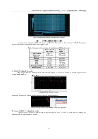
Below fig 17 gives information about the power consumption of 1kb cache array. We achieve almost 54% power reduction.
Table III Summary of Conventional 6T and Dynamic 8T 1kb array power consumption results
Conventional Proposed
SRAM 6T SRAM 8T
Power 1.12094mW 519.1476µW
consumption
Fig 17. 1kb cache power consumption comparasion.
VIII. CONCLUSION
A 8T SRAM with a column-based dynamic supply has been proposed. Analyse both conventional 6T and
proposed SRAM using N-curve. The proposed SRAM 8T cell has achieved improved read stability, low power, read current
and leakage current. N-curve metric was best method to analysis the cell stability it contains both voltage and current
information. So, we can analysis the cell stability correct way. Above results prove that 54% of the power is reduced and
read stability of proposed cell achieve double amount approximately with comparing SRAM 6T cell.
REFERENCES
[1]. Do Anh-Tuan, Jeremy Yung Shern Low, Joshua Yung Lih Low, Zhi-Hui Kong, Xiaoliang Tan, and Kiat-SengYeo,‖An 8T
Differential SRAM With Improved NoiseMargin for Bit-Interleaving in 65 nm CMOS‖ IEEE Transnctions on circuits and
systems—I :regular papers, Vol. 58, No. 6, june 2011.
[2]. E. Grossaret al., ―Read stability and write-ability analysis of SRAM cells for nanometer technologies,‖ IEEE J. Solid-State
Circuits, vol.41, no. 11, pp. 2577–2588, Nov. 2006.
[3]. A. Silet al., ―A novel 8T SRAM cell with improved read-snm,‖ in Proc. NEWCAS, 2007, pp. 1289–1292.
[4]. Jan M. Rabaey,AnanthaChandrakasan and BorivojeNikolic, ‖Digital Integrated Circuits‖, ISBN 81-7808-991-2, Pearson
Education, 2003.
[5]. Neil H.E.Weste,David Harris and Ayan Banerjee, ―CMOS VLSI Design, a circuits and systems perspective‖ ,ISBN:
0321149017/9780321149015Third edition, Pearson Education, 2005.
7