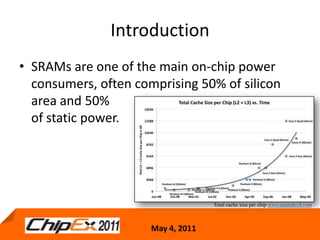
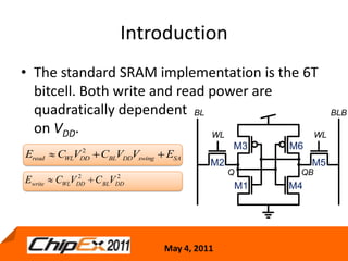
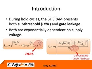
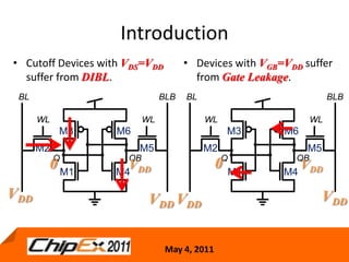
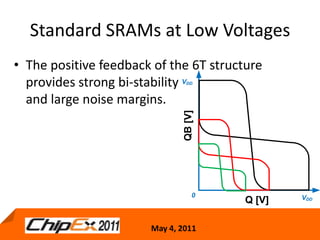
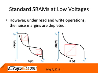
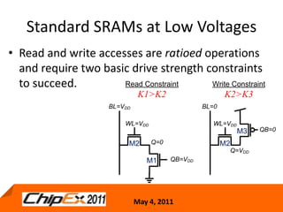
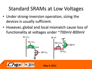
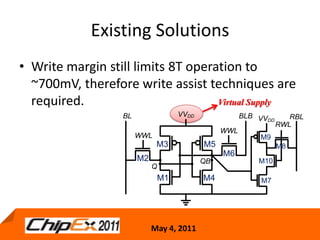
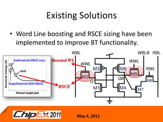
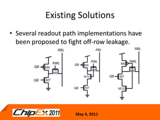
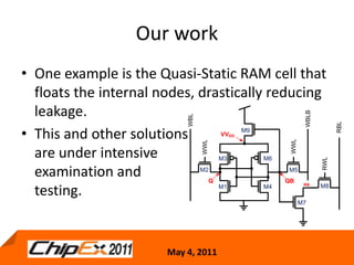
Low Voltage SRAM DesignChallenges and SolutionsAdam Teman, Janna Mezhibovsky, Dr. Alexander FishLow Power Circuits and Systems Lab (LPC&S)The VLSI Systems CenterBen-Gurion UniversityMay 4, 2011
Lecture ContentsIntroductionStandard SRAMs at Low VoltagesExisting SolutionsLPC&S SRAM Design Activities
IntroductionSRAMs are one of the main on-chip power consumers, often comprising 50% of silicon area and 50% of static power.3Total cache size per chip www.anandtech.com
IntroductionThe standard SRAM implementation is the 6T bitcell. Both write and read power are quadratically dependenton VDD.4
IntroductionDuring hold cycles, the 6T SRAM presents both subthreshold (DIBL) and gateleakage.Both are exponentially dependent on supply voltage.5DIBLGate Bias and Oxide Thickness
Cutoff Devices with VDS=VDD suffer from DIBL.Devices with VGB=VDD suffer from Gate Leakage.00VDDVDDVDDVDDVDDVDDIntroduction6
IntroductionThe best way to aggressively reduce SRAM power is to lower the operating voltage.Quadratic reduction of Dynamic PowerExponential Reduction of DIBLExponential Reduction of Gate Leakage7
Standard SRAMs at Low VoltagesThe positive feedback of the 6T structure provides strong bi-stability and large noise margins.8
Standard SRAMs at Low VoltagesHowever, under read and write operations, the noise margins are depleted.9
Standard SRAMs at Low VoltagesRead and write accesses are ratioed operations and require two basic drive strength constraintsto succeed.10
Standard SRAMs at Low VoltagesUnder strong-inversion operation, sizing the devices is usually sufficient.However, global and local mismatch cause loss of functionality at voltages under ~700mV-800mV11
Existing SolutionsThe basic solution to the read margin problem is decoupling the readout path.12
Existing SolutionsA differential decoupled readout provides better Sense Amplifier operation:13
Existing SolutionsWrite margin still limits 8T operation to ~700mV, therefore write assist techniques are required.	14Virtual Supply
Existing SolutionsWord Line boosting and RSCE sizing have been implemented to improve 8T functionality.15Boosted WLRSCE
Existing SolutionsSeveral readout path implementations have been proposed to fight off-row leakage.16
Our workVery few groups have tried to “think outside the box” and modify the internal cell structure.We have proposed an internal supply feedback concept that cuts off the supply to reduce internal leakage.17
Our workOne example is the Quasi-Static RAM cell that floats the internal nodes, drastically reducing leakage.This and other solutionsare under intensiveexamination and testing.18
Questions?19

Track e low voltage sram - adam teman bgu

  • 1.
    Low Voltage SRAMDesignChallenges and SolutionsAdam Teman, Janna Mezhibovsky, Dr. Alexander FishLow Power Circuits and Systems Lab (LPC&S)The VLSI Systems CenterBen-Gurion UniversityMay 4, 2011
  • 2.
    Lecture ContentsIntroductionStandard SRAMsat Low VoltagesExisting SolutionsLPC&S SRAM Design Activities
  • 3.
    IntroductionSRAMs are oneof the main on-chip power consumers, often comprising 50% of silicon area and 50% of static power.3Total cache size per chip www.anandtech.com
  • 4.
    IntroductionThe standard SRAMimplementation is the 6T bitcell. Both write and read power are quadratically dependenton VDD.4
  • 5.
    IntroductionDuring hold cycles,the 6T SRAM presents both subthreshold (DIBL) and gateleakage.Both are exponentially dependent on supply voltage.5DIBLGate Bias and Oxide Thickness
  • 6.
    Cutoff Devices withVDS=VDD suffer from DIBL.Devices with VGB=VDD suffer from Gate Leakage.00VDDVDDVDDVDDVDDVDDIntroduction6
  • 7.
    IntroductionThe best wayto aggressively reduce SRAM power is to lower the operating voltage.Quadratic reduction of Dynamic PowerExponential Reduction of DIBLExponential Reduction of Gate Leakage7
  • 8.
    Standard SRAMs atLow VoltagesThe positive feedback of the 6T structure provides strong bi-stability and large noise margins.8
  • 9.
    Standard SRAMs atLow VoltagesHowever, under read and write operations, the noise margins are depleted.9
  • 10.
    Standard SRAMs atLow VoltagesRead and write accesses are ratioed operations and require two basic drive strength constraintsto succeed.10
  • 11.
    Standard SRAMs atLow VoltagesUnder strong-inversion operation, sizing the devices is usually sufficient.However, global and local mismatch cause loss of functionality at voltages under ~700mV-800mV11
  • 12.
    Existing SolutionsThe basicsolution to the read margin problem is decoupling the readout path.12
  • 13.
    Existing SolutionsA differentialdecoupled readout provides better Sense Amplifier operation:13
  • 14.
    Existing SolutionsWrite marginstill limits 8T operation to ~700mV, therefore write assist techniques are required. 14Virtual Supply
  • 15.
    Existing SolutionsWord Lineboosting and RSCE sizing have been implemented to improve 8T functionality.15Boosted WLRSCE
  • 16.
    Existing SolutionsSeveral readoutpath implementations have been proposed to fight off-row leakage.16
  • 17.
    Our workVery fewgroups have tried to “think outside the box” and modify the internal cell structure.We have proposed an internal supply feedback concept that cuts off the supply to reduce internal leakage.17
  • 18.
    Our workOne exampleis the Quasi-Static RAM cell that floats the internal nodes, drastically reducing leakage.This and other solutionsare under intensiveexamination and testing.18
  • 19.