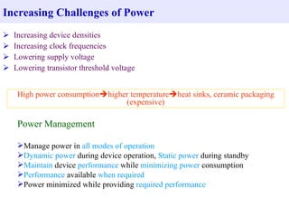
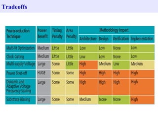
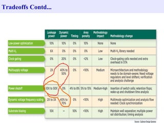
1. Low power techniques aim to reduce both dynamic and static/leakage power in integrated circuits. Dynamic power is reduced through techniques like lowering supply voltage and clock frequency, while leakage power is reduced by increasing transistor threshold voltage.
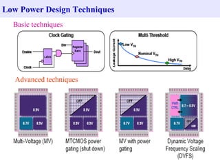
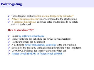
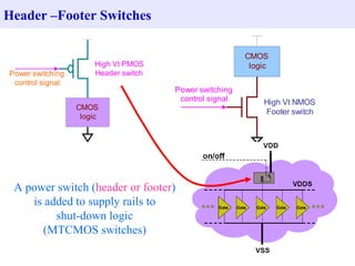
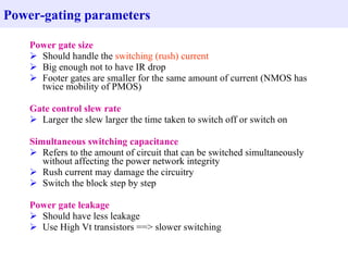
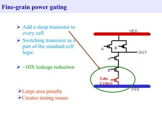
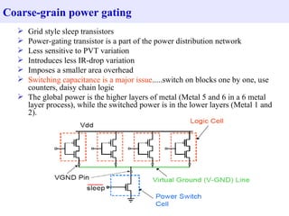
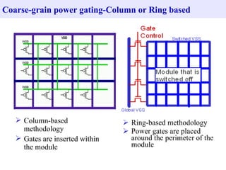
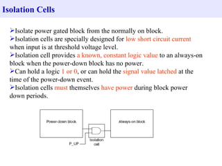
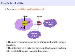
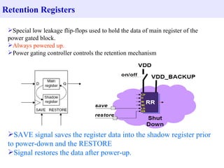
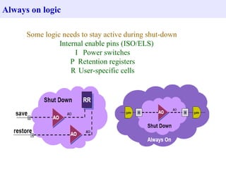
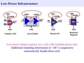
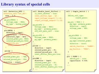
2. Power gating is a widely used technique that temporarily turns off unused circuit blocks to drastically reduce leakage power. It requires additional power switches and isolation cells to safely turn blocks on and off.
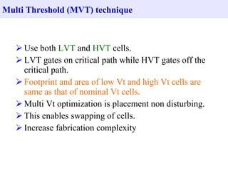
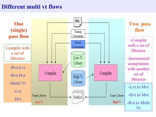
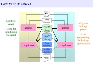
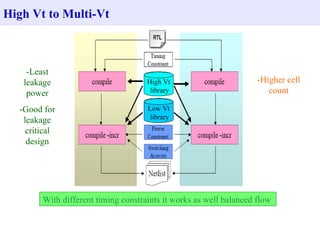
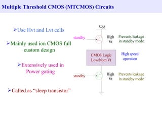
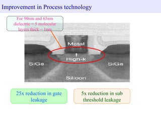
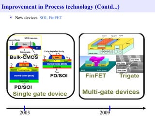
3. Multi-threshold CMOS uses both low and high threshold voltage transistors optimized for performance and leakage respectively. Further scaling presents new challenges as leakage power becomes dominant.