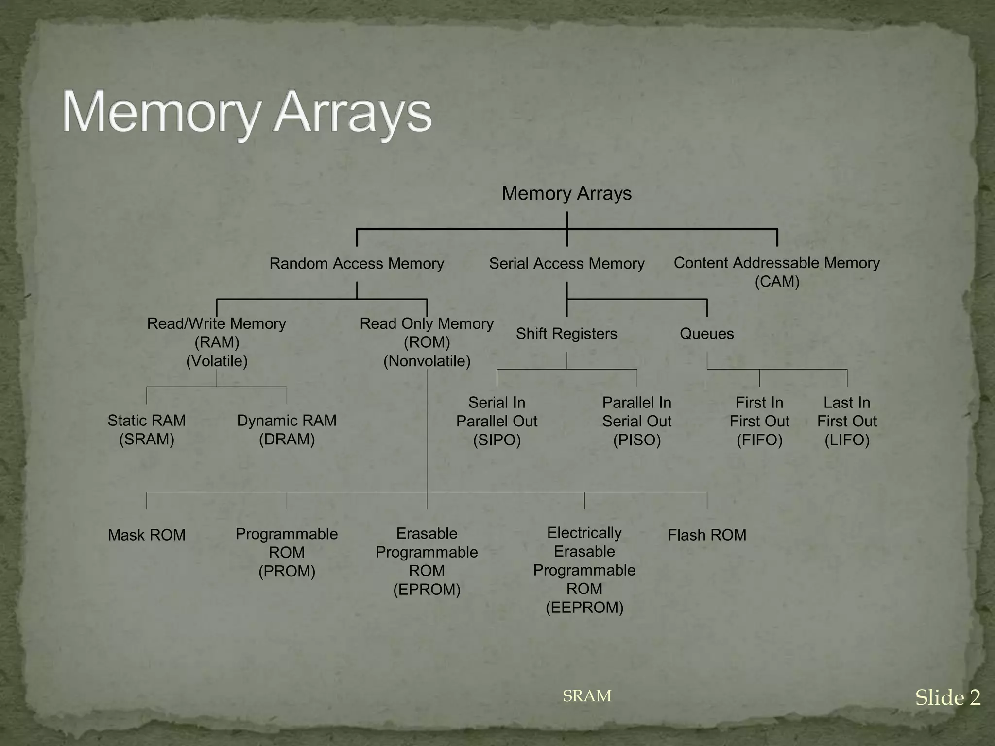
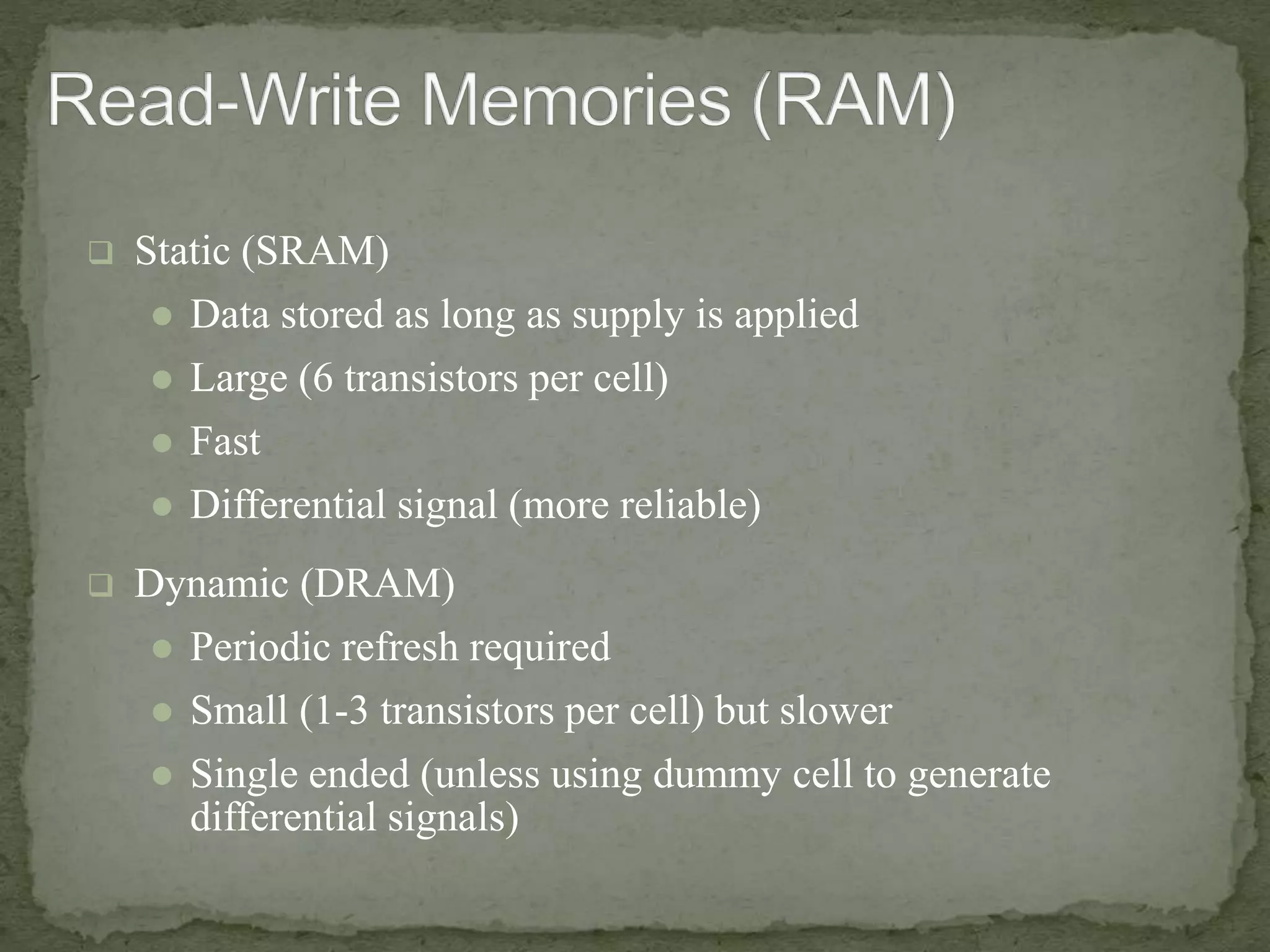
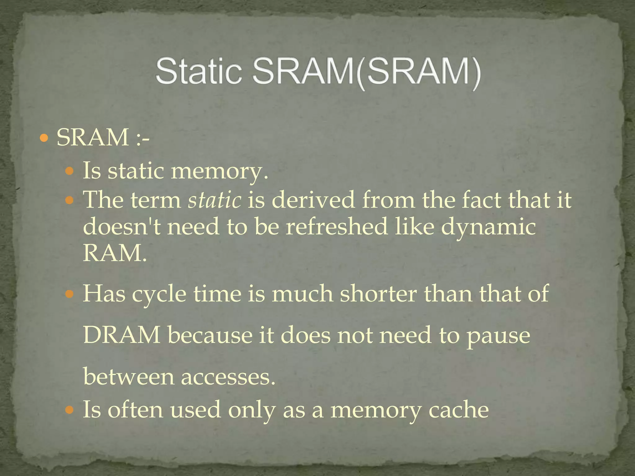
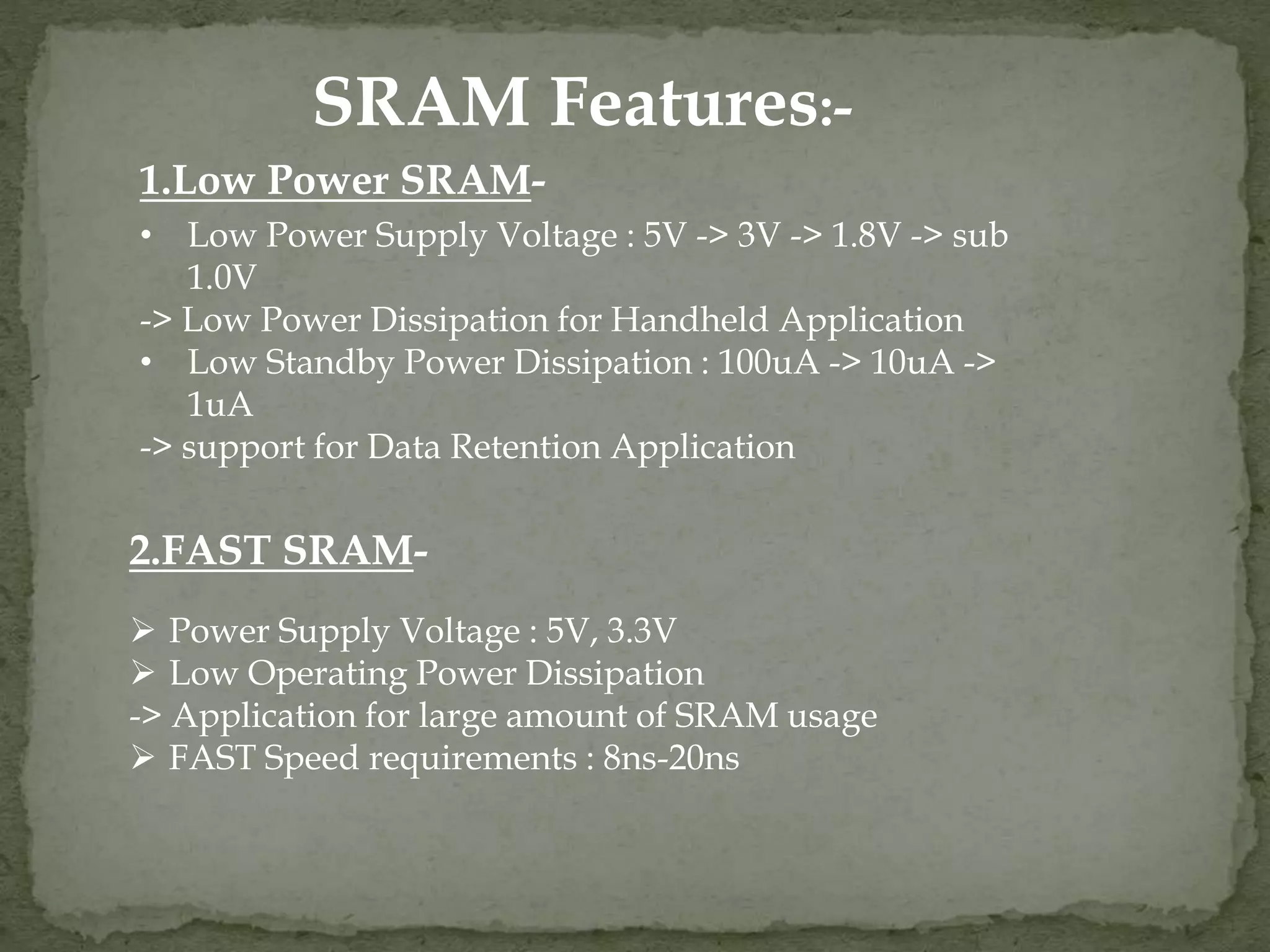
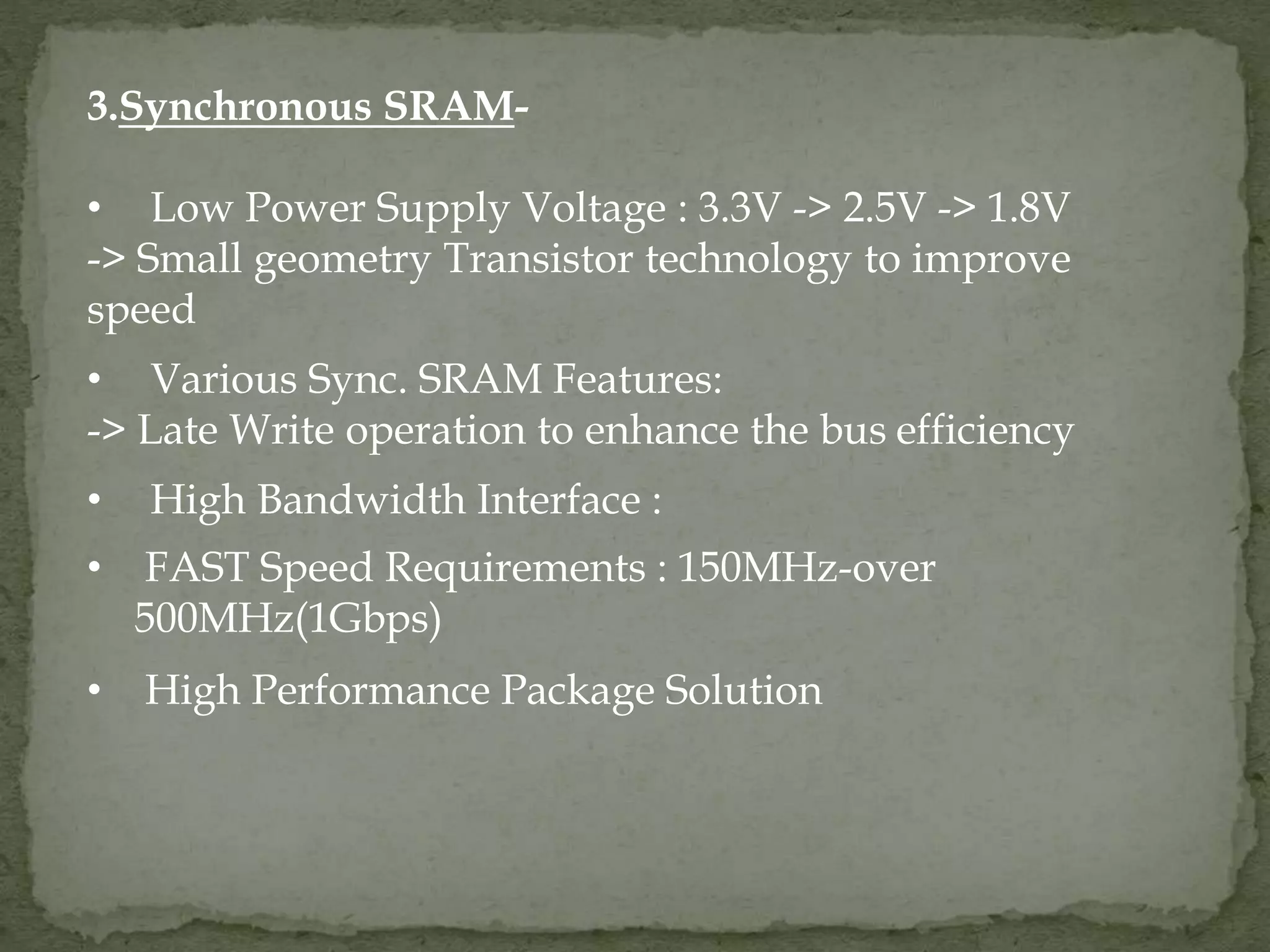
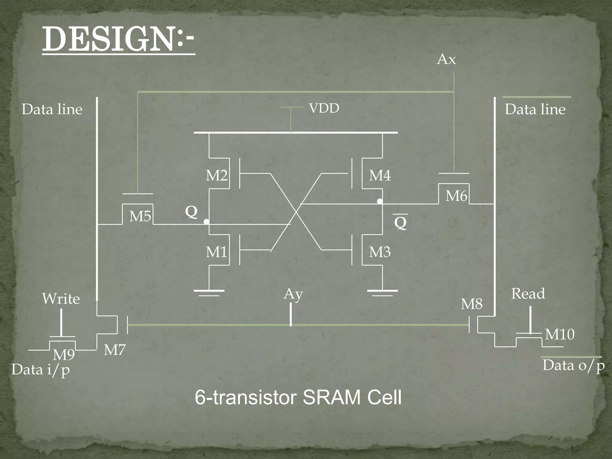
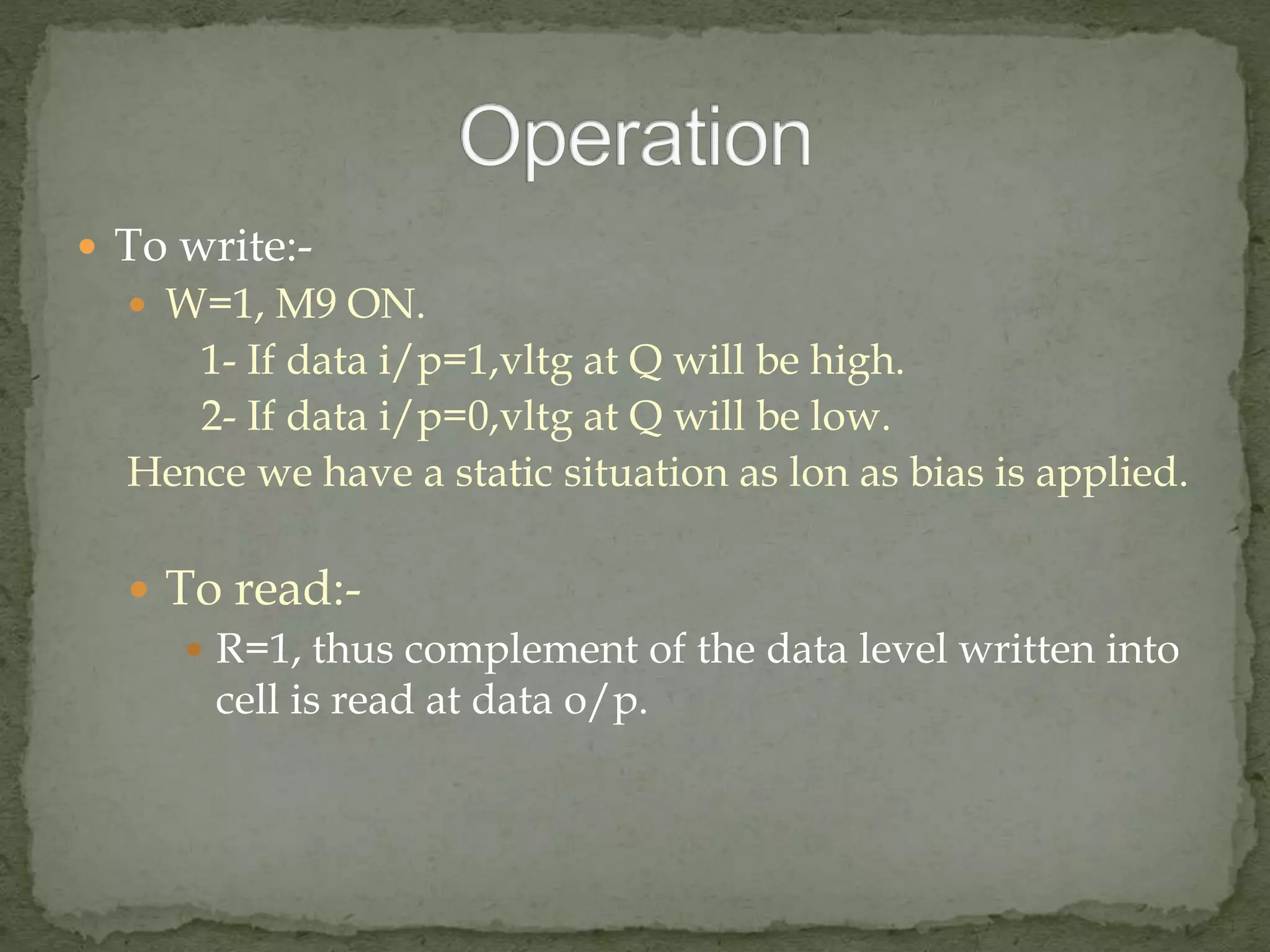
The document discusses different types of memory, focusing on Static Random Access Memory (SRAM), which does not require refreshing like Dynamic RAM (DRAM) and is used primarily as a cache due to its fast access times. It details SRAM features, including low power, fast operation, and various types, such as bipolar, NMOS, Bi-CMOS, and CMOS, highlighting their applications and advantages. Additionally, it outlines SRAM's characteristics, benefits, and typical uses in industrial systems and consumer electronics.
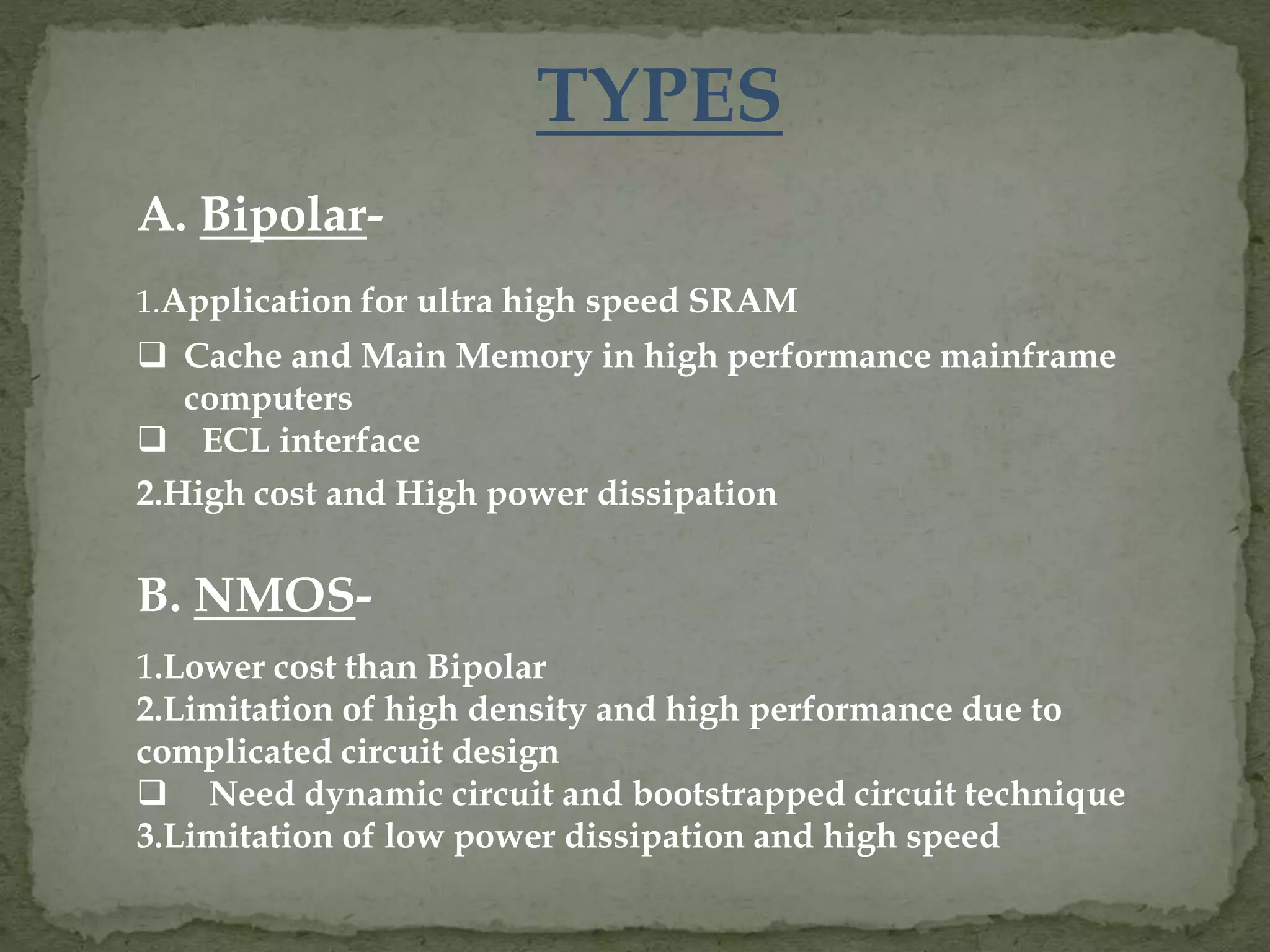
![C. Bi-CMOS-
- High speed
. application for small volume/high performance
- Complicated process [7][8]
. use triple diffused BiCMOS process
- Limitation of low power supply voltage [9]
. improve the MOS Transistor (Lower Vth)
. use BiNMOS or NBiCMOS
. Base boost technique
D. CMOS-
1. Low cost and low power dissipation
2. Easy to make high density SRAM
3.Limitation of high speed
Improve the MOS Transistor
Use Dynamic Gate Logic](https://image.slidesharecdn.com/sram-140916072356-phpapp01/75/SRAM-10-2048.jpg)