Download to read offline
![DESIGN AND ANALYSIS OF LOW POWER SUB-THRESHOLD SRAM
22
VII. CONCLUSION
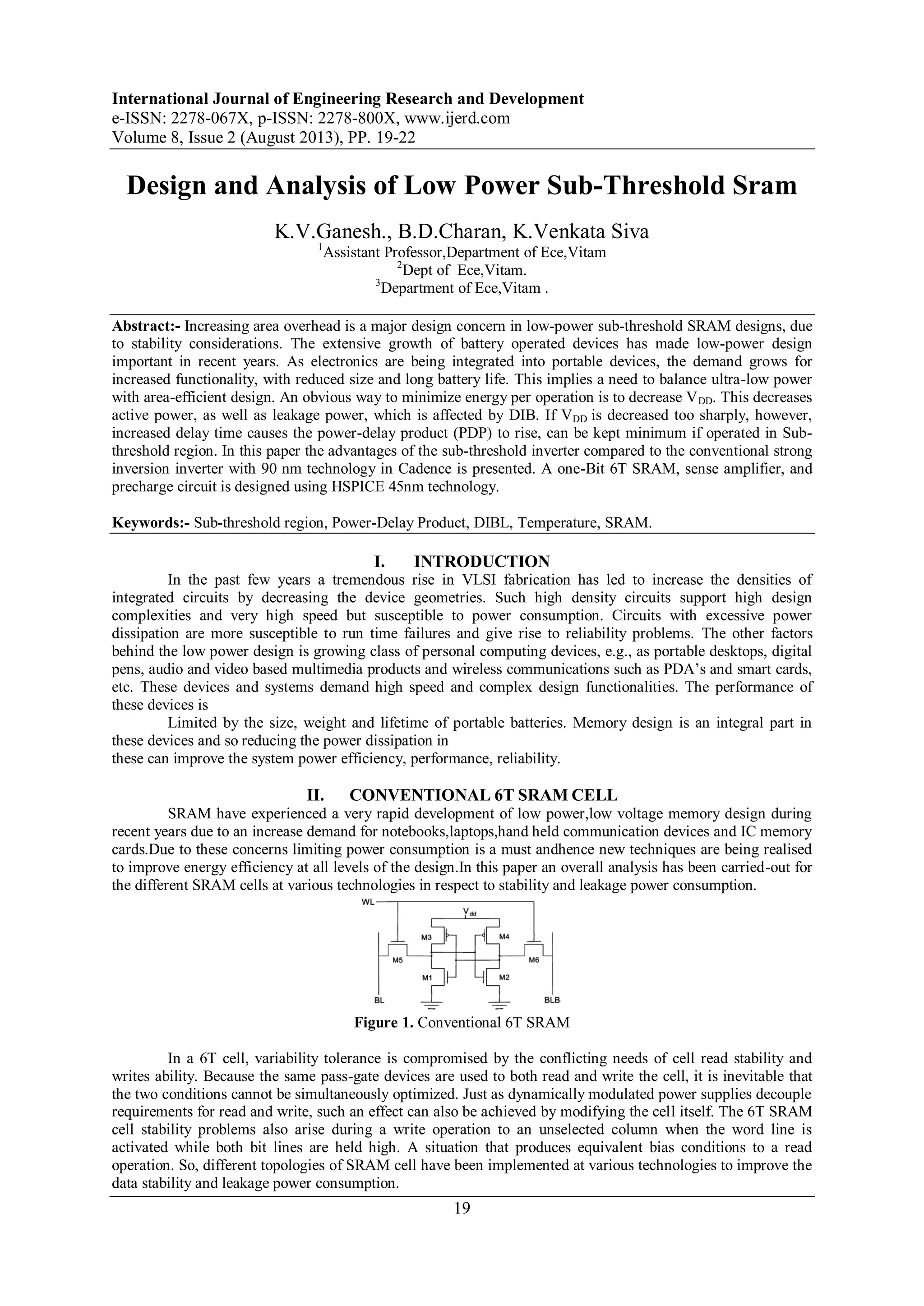
In this, I made comparisons between different configurations of SRAMs. In all configurations 4T, 6T,
8T, 9T SRAMs SNM is the problem when scaling the voltages. In 10T SRAM we can find optimum power and
optimum delay as well as good SNM. 10 T SRAM achieves best stability and low power compared to remaining
configurations in 45nm. Read and write operations done for all configurations.
REFERENCES
[1] M.E. Sinangil, N. Verma, and A.P. Chandrakasan, ‘‘A Reconfigurable 8T Ultra-Dynamic Voltage
Scalable (U-DVS) SRAM in 65 nm CMOS,’’ IEEE J. Solid-State Circuits, vol. 44, no. 11, 2009, pp.
3163-3173.
[2] K. Takeda et al., ‘‘A Read-Static-Noise-Margin-Free SRAM Cell for Low-VDD and High-Speed
Applications,’’ IEEE J. Solid-State Circuits, vol. 41, no. 1, 2006, pp. 113-121.
[3] B.H. Calhoun and A.P. Chandrakasan, ‘‘A 256-kb 65-nm Sub-threshold SRAM Design for Ultra-Low-
Voltage Operation,’’ IEEE J. Solid-State Circuits, vol. 42, no. 3, 2007, pp. 680-688
[4] I.J. Chang et al., ‘‘A 32 kb 10T Sub-threshold SRAM Array with Bit-Interleaving and Differential
Read Scheme in 90 nm CMOS,’’ IEEE J. Solid-State Circuits, vol. 44, no. 2, 2009, pp. 650-658.
[5] H. Pilo et al., ‘‘An SRAM Design in 65-nm Technology Node Featuring Read and Write-Assist
Circuits to Expand Operating Voltage,’’ IEEE J. Solid-State Circuits, vol. 42, no. 4, 2007, pp. 813-819.
[6] M. Qazi et al., ‘‘A 512kb 8T SRAM Macro Operating down to 0.57V with an AC-Coupled Sense
Amplifier and Embedded Data-Retention-Voltage Sensor in 45nm SOI CMOS,’’ Proc. IEEE Int’l
Solid-State Circuits Conf. (ISSCC 10), 2010, pp. 350-351.
[7] H. Qin et al., ‘‘SRAM Leakage Suppression by Minimizing Standby Supply Voltage,’’ Proc. 5th Int’l
Symp. Quality Electronic Design (ISQED 04), IEEE Press, 2004,pp. 55-60.
[8] S. Ohbayashi et al., ‘‘A 65-nm SoC Embedded 6T-SRAM Designed for Manufacturability with Read
and Write Operation Stabilizing Circuits,’’ IEEE J. Solid-State Circuits, vol. 42, no. 4, 2007, pp. 820-
829.
[9] Y. Morita et al., ‘‘An Area-Conscious Low-Voltage- Oriented 8T-SRAM Design under DVS
Environment,’’ Proc. IEEE Symp. VLSI Circuits, IEEE Press, 2007, pp. 256-257.](https://image.slidesharecdn.com/c08021922-130815042847-phpapp02/85/International-Journal-of-Engineering-Research-and-Development-IJERD-4-320.jpg)

The document discusses the design and analysis of low-power sub-threshold SRAM, highlighting the challenges of area overhead and stability in SRAM designs due to the increasing demand for efficient battery-operated devices. It compares various SRAM configurations (4T, 6T, 8T, 9T, and 10T) and concludes that the 10T SRAM offers the best stability, low power consumption, and optimum delay in a 45nm technology context. The paper suggests that separating read and write operations can enhance performance and stability in SRAM designs.