As there is a demand for portable electronic systems or devices, there is an incremental growth in the technology in the past few decades and also technology is cumulative at a random rate, devices are consuming large amount of power due to this the life of the battery is draining fast. so there must be a alternative devices or circuits which can reduce the power by efficiently maintaining the area and performance, therefore life of battery can be increased. As SRAM is the heart of block in all the electronic design, where the power consumption is maximum there by analyzing, estimating & modifying or changing the logic, will be able to reduce the power and performance can be greatly achieved. This proposal describes under the principle of ultra-low power logic approach which operates under subthreshold voltage operating which leads to lower power and also efficient in functionality along with secondary constraints.
The International Journal of Engineering and Science (The IJES)theijes
The International Journal of Engineering & Science is aimed at providing a platform for researchers, engineers, scientists, or educators to publish their original research results, to exchange new ideas, to disseminate information in innovative designs, engineering experiences and technological skills. It is also the Journal's objective to promote engineering and technology education. All papers submitted to the Journal will be blind peer-reviewed. Only original articles will be published.
A Comparitive Analysis of Improved 6t Sram Cell With Different Sram CellIJERA Editor
High speed and low power consumption have been the primary issue to design Static Random Access Memory (SRAM), but we are facing new challenges with the scaling of technology. The stability and speed of SRAM are important issues to improve efficiency and performance of the system. Stability of the SRAM depends on the static noise margin (SNM) so the noise margin is also important parameter for the design of memory because the higher noise margin confirms the high speed of the SRAM cell. In this paper, the improved 6T SRAM cell shows maximum reduction in power consumption of 88%, maximum reduction in delay of 64% and maximum SNM of 17% increases compared with 7T SRAM cell.
An Innovative Design solution for minimizing Power Dissipation in SRAM CellIJERA Editor
Over the years, the development of the logic on the chip is increased. To sustain and drive the logic flow, various techniques and SRAM cell designs have been implemented. The basic element of memory design is 6T SRAM cell. But while dealing with this 6T SRAM cell there are some issues with the parametric analysis on the performance of the cell. This paper presents an innovative design idea of new 8T RAM cell with various parametric analysis. The proposed cell is compared with the standard cell in terms of different parameters such as area, speed and power consumption along with the loading effect with the increase in load capacitance on the cell. The structure is designed with CMOS 45 nm Technology with BSIM 4 MOS modelling using Microwind 3.5 software tool
Implementation of High Reliable 6T SRAM Cell Designiosrjce
Memory can be formed with the integration of large number of basic storing element called cells.
SRAM cell is one of the basic storing unit of volatile semiconductor memory that stores binary logic '1' or '0' bit.
Modified read and write circuits were proposed in this paper to address incorrect read and write operations in
conventional 6T SRAM cell design available in open literature. Design of a new highly reliable 6T SRAM cell
design is proposed with reliable read, write operations and negative bit line voltage (NBLV). Simulations are
carried out using MENTOR GRAPHICS
In the project#1, IBM 130nm process is used to design and manual layout a 128 word SRAM, with word size 10bits. Cadence's Virtuoso is applied for layout editing, DRC and LVS running and circuit simulation.
International Journal of Engineering Research and Development (IJERD)IJERD Editor
journal publishing, how to publish research paper, Call For research paper, international journal, publishing a paper, IJERD, journal of science and technology, how to get a research paper published, publishing a paper, publishing of journal, publishing of research paper, reserach and review articles, IJERD Journal, How to publish your research paper, publish research paper, open access engineering journal, Engineering journal, Mathemetics journal, Physics journal, Chemistry journal, Computer Engineering, Computer Science journal, how to submit your paper, peer reviw journal, indexed journal, reserach and review articles, engineering journal, www.ijerd.com, research journals,
yahoo journals, bing journals, International Journal of Engineering Research and Development, google journals, hard copy of journal
Design and Simulation Low power SRAM Circuitsijsrd.com
SRAMs), focusing on optimizing delay and power. As the scaling trends in the speed and power of SRAMs with size and technology and find that the SRAM delay scales as the logarithm of its size as long as the interconnect delay is negligible. Non-scaling of threshold mismatches with process scaling, causes the signal swings in the bitlines and data lines also not to scale, leading to an increase in the relative delay of an SRAM, across technology generations. Appropriate methods for reduction of power consumption were studied such as capacitance reduction, very low operating voltages, DC and AC current reduction and suppression of leakage currents to name a few.. Many of reviewed techniques are applicable to other applications such as ASICs, DSPs, etc. Battery and solar-cell operation requires an operating voltage environment in low voltage area. These conditions demand new design approaches and more sophisticated concepts to retain high device reliability. The proposed techniques (USRS and LPRS) are topology based and hence easier to implement.
Energy optimization of 6T SRAM cell using low-voltage and high-performance in...IJECEIAES
The performance of the cell deteriorates, when static random access memory (SRAM) cell is operated below 1V supply voltage with continuous scale down of the complementary metal oxide semiconductor (CMOS) technology. The conventional 6T, 8T-SRAM cells suffer writeability and read static noise margins (SNM) at low-voltages leads to degradation of cell stability. To improve the cell stability and reduce the dynamic power dissipation at low- voltages of the SRAM cell, we proposed four SRAM cells based on inverter structures with less energy consumption using voltage divider bias current sink/source inverter and NOR/NAND gate using a pseudo-nMOS inverter. The design and implementation of SRAM cell using proposed inverter structures are compared with standard 6T, 8T and ST-11T SRAM cells for different supply voltages at 22-nm CMOS technology exhibit better performance of the cell. The read/write static noise margin of the cell significantly increases due to voltage divider bias network built with larger cell-ratio during read path. The load capacitance of the cell is reduced with minimized switching transitions of the devices during high-to-low and low- to-high of the pull-up and pull-down networks from VDD to ground leads to on an average 54% of dynamic power consumption. When compared with the existing ones, the read/write power of the proposed cells is reduced to 30%. The static power gets reduced by 24% due to stacking of transistors takes place in the proposed SRAM cells as compare to existing ones. The layout of the proposed cells is drawn at a 45-nm technology, and occupies an area of 1.5 times greater and 1.8 times greater as compared with 6T-SRAM cell.
IJERA (International journal of Engineering Research and Applications) is International online, ... peer reviewed journal. For more detail or submit your article, please visit www.ijera.com
PERFORMANCE EVALUATION OF DIFFERENT SRAM CELL STRUCTURES AT DIFFERENT TECHNOL...VLSICS Design
In recent years the demand for low power devices has been increases tremendously. To solve the power dissipation problem, many researchers have proposed different ideas from the device level to the architectural level and above. However, there is no universal way to avoid tradeoffs between power, delay and area, thus designers are required to choose appropriate techniques that satisfy application and product needs. The demand for static random-access memory (SRAM) is increasing with large use of SRAM in System On-Chip and high-performance VLSI circuits. This paper represents the simulation of different SRAM cells and their comparative analysis on different parameters such as Power Supply Voltage, area efficiency etc to enhance the performance. All the simulations have been carried out on BSIM 3V3 90nm, 45nm and 32 technology at Tanner EDA tool.
A Novel Low Power Energy Efficient SRAM Cell With Reduced Power Consumption u...iosrjce
In modern high performance integrated circuits, maximum of the total active mode energy is
consumed due to leakage current. SRAM cell array is main source of leakage current since majority of
transistor are utilized for on-chip memory in today high performance microprocessor and system on chip
designs. Therefore the design of low leakage SRAM is required. Reducing power dissipation, supply voltage,
leakage currents, area of chip are the most important parameters in today`s VLSI designs. But scaling of these
parameters will lead to drastic increase in sub threshold leakage currents and power dissipation because of that
performance of the design is degraded. So to overcome these issues it is better to concentrate on reduction of
active leakage currents and dynamic power dissipation by using power reduction techniques. In this paper 9T
SRAM (data retention p-gated) cell for low voltage and energy constrain application is analyzed with respect to
power dissipation, area and delay. The analyzed design of 9T SRAM cell with MTCMOS technique has been
proposed. Designed circuits are simulated in Microwind 3.1 VLSI CAD Tool in 90 and 65nm CMOS technology.
A Single-Ended With Dynamic Feedback Control 8T Subthreshold SRAM Cell Ieee Xpert
A Single-Ended With Dynamic Feedback Control
8T Subthreshold SRAM Cell
A Single-Ended With Dynamic Feedback Control
8T Subthreshold SRAM Cell
A Single-Ended With Dynamic Feedback Control
8T Subthreshold SRAM Cell
A Single-Ended With Dynamic Feedback Control
8T Subthreshold SRAM Cell
A Single-Ended With Dynamic Feedback Control
8T Subthreshold SRAM Cell
IJRET : International Journal of Research in Engineering and Technology is an international peer reviewed, online journal published by eSAT Publishing House for the enhancement of research in various disciplines of Engineering and Technology. The aim and scope of the journal is to provide an academic medium and an important reference for the advancement and dissemination of research results that support high-level learning, teaching and research in the fields of Engineering and Technology. We bring together Scientists, Academician, Field Engineers, Scholars and Students of related fields of Engineering and Technology
Power analysis of 4 t sram by stacking technique using tanner tooleSAT Publishing House
IJRET : International Journal of Research in Engineering and Technology is an international peer reviewed, online journal published by eSAT Publishing House for the enhancement of research in various disciplines of Engineering and Technology. The aim and scope of the journal is to provide an academic medium and an important reference for the advancement and dissemination of research results that support high-level learning, teaching and research in the fields of Engineering and Technology. We bring together Scientists, Academician, Field Engineers, Scholars and Students of related fields of Engineering and Technology
IJERA (International journal of Engineering Research and Applications) is International online, ... peer reviewed journal. For more detail or submit your article, please visit www.ijera.com
250nm Technology Based Low Power SRAM Memoryiosrjce
High integration density, low power and fastperformance are all critical parameters in designing of
memory blocks. Static Random Access Memories (SRAMs)’s focusing on optimizing dynamic power concept of
virtual source transistors is used for removing direct connection between VDD and GND.
Also stacking effect can be reduced by switching off the stacktransistors when the memory is ideal and the
leakage current using SVL techniques This paper discusses the evolution of 9t SRAM circuits in terms of low
power consumption, The whole circuit verification is done on the Tanner tool, Schematic of the
SRAM cell is designed on the S-Edit and net list simulation done by using T-spice and waveforms are analyzed
through the W-edit
Average and Static Power Analysis of a 6T and 7T SRAM Bit-Cell at 180nm, 90nm...idescitation
A lot of consideration has been given to problems arising due to power dissipation.
Different ideas have been proposed by many researchers from the device level to the
architectural level and above. However, there is no universal way to avoid tradeoffs between
the power, delay and area. This is why; the designers are required to choose appropriate
techniques that satisfy application and product needs. Another important component of
power which contributes to power dissipation is Dynamic Power. This power is increasing
due to prolonged use of the electronic equipments. This is due to the fact that now-a-days
people are working on electronic systems from morning till night; it may be a mobile phone
or a laptop or any other equipment. This paper deals with the estimation of two components
of power i.e. static power (when device is in the standby mode) and the average power
(average amount of energy consumed with respect to time) of a 6T and 7T SRAM (Static
Random Access Memory) bit-cell at 180nm, 90nm, and 45nm CMOS Technology. This is
done in order to estimate the power required for a high speed operation of 6T and 7T
SRAM bit-cell.
Implementation of an Efficient SRAM for Ultra-Low Voltage Application Based o...IOSR Journals
Abstract: Operation of standard 6T static random access memory (SRAM) cells at sub or near threshold
voltages is unfeasible, predominantly due to degraded static noise margins (SNM) and poor robustness. We
analyze Schmitt-Trigger (ST)-based differential-sensing static random access memory (SRAM) bitcells for
ultralow-voltage operation. The ST-based SRAM bitcells address the fundamental conflicting design
requirement of the read versus write operation of a conventional 6T bitcell. The ST operation gives better readstability
as well as better write-ability compared to the standard 6T bitcell. In this paper we are going to
propose a new SRAM bitcell for the purpose of read stability and write ability by using 90nm technology , and
less power consumption, less area than the existing Schmitt trigger1 based SRAM. Design and simulations were done using DSCH and Microwind.
Index Terms: read stability, write ability, Schmitt trigger.
IJERA (International journal of Engineering Research and Applications) is International online, ... peer reviewed journal. For more detail or submit your article, please visit www.ijera.com
Static-Noise-Margin Analysis of Modified 6T SRAM Cell during Read Operationidescitation
As modern technology is spreading fast, it is very
important to design low power, high performance, fast
responding SRAM(Static Random Access Memory) since they
are critical component in high performance processors. In
this paper we discuss about the noise effect of different SRAM
circuits during read operation which hinders the stability of
the SRAM cell. This paper also represents a modified 6T
SRAM cell which increases the cell stability without
increasing transistor count.
“Power and Temperature Analysis of 12T CMOS SRAM Designed With Short Channel ...iosrjce
This paper focuses mainly on dynamic power dissipations at different temperature for both read and
write operations of 12T SRAM. In the proposed 12T structure virtual vdd concept is employed because of this
leakage current will reduce. Hence reduction in leakage current causes reduction in dynamic power. Power
dissipation of the proposed SRAM cell have been determined and compared to those of some other existing
memory cells. Proposed cell is a short channel BSIM4 model. It is observed that power dissipation of 12T
SRAM for read operation at 40̊
̊
is 44.7nw and for write operation it is 38.79nw. The proposed SRAM cell
dissipates less power. Simulation has been done in Tanner-13 EDA tool for 50nm.
IOSR journal of VLSI and Signal Processing (IOSRJVSP) is an open access journal that publishes articles which contribute new results in all areas of VLSI Design & Signal Processing. The goal of this journal is to bring together researchers and practitioners from academia and industry to focus on advanced VLSI Design & Signal Processing concepts and establishing new collaborations in these areas.
IJERA (International journal of Engineering Research and Applications) is International online, ... peer reviewed journal. For more detail or submit your article, please visit www.ijera.com
International Journal of Engineering Research and Applications (IJERA) is an open access online peer reviewed international journal that publishes research and review articles in the fields of Computer Science, Neural Networks, Electrical Engineering, Software Engineering, Information Technology, Mechanical Engineering, Chemical Engineering, Plastic Engineering, Food Technology, Textile Engineering, Nano Technology & science, Power Electronics, Electronics & Communication Engineering, Computational mathematics, Image processing, Civil Engineering, Structural Engineering, Environmental Engineering, VLSI Testing & Low Power VLSI Design etc.
IJRET : International Journal of Research in Engineering and Technology is an international peer reviewed, online journal published by eSAT Publishing House for the enhancement of research in various disciplines of Engineering and Technology. The aim and scope of the journal is to provide an academic medium and an important reference for the advancement and dissemination of research results that support high-level learning, teaching and research in the fields of Engineering and Technology. We bring together Scientists, Academician, Field Engineers, Scholars and Students of related fields of Engineering and Technology.
PCI Express (Peripheral Component Interconnect Express) abbreviated as PCIe or PCI-E, is designed to replace the older PCI, PCI-X, AGP standards. We present a data communication developed system for use the transfer data between the host and the peripheral devices via PCIe. The performance and the available area on the board are effective by using the PCIe. PCIe is a serial expansion bus interconnection method which is use for high speed communication. PCI Express represents the currently fastest and most expensive solution to connect the peripheral devices with general purpose CPU. It provides a highest bandwidth connection in the PC platform. In this paper, we highlight the different types of bus architecture. Here the PCIe architecture is described how data transfer between the CPU to the destination.
Implementation of Area & Power Optimized VLSI Circuits Using Logic TechniquesIOSRJVSP
To achieve the reduction of power consumption, optimizations are required at various levels of the design steps such as algorithm, architecture, logic and circuit & process techniques. This paper considers the two logic level approaches for low power digital design. Optimization techniques are carried to reduce switching activity power of individual logic-gates. we can reduce the power by using either circuit level optimization or logical level optimization. In this paper, the circuit level optimization process is followed to reduce the area and power. In the first approach, Modified gate diffusion input (GDI) logic is used in the proposed parallel asynchronous self time adder (PASTA) technique. Similarly, the structure of XOR gate and half adder is reduced to achieve the low area and low power. In second approach, Multi value logic based digital circuit is designed by increasing the representation domain from the two level (N=2) switching algebra to N > 2 levels. The main advantage of this approach is to compensate the inefficiency of existing integrated circuits that are used to implement the universal set of MVL gates. From the results, the proposed GDL logic based Adder offers less number of transistors (area) and low power consumption than the existing technique. And proposed MVL technique allows designing MVL digital circuit that is set to obtain the values from the binary circuits. Also this technique offers low power and small wiring delay, when compared to binary and three value logic. The simulation process is carried out by tanner toolv14.11 to check the functionality of the PASTA & MVL circuits.
Design of Low Voltage D-Flip Flop Using MOS Current Mode Logic (MCML) For Hig...IOSRJVSP
This paper presents a new topology to implement MOS current mod logic (MCML) tri-state buffers. In Mos current mode logic (MCML) current section is improves the performance and maintains low power of the circuit. MCML circuits contains true differential operation by which provides the feature of low noise level generation and static power dissipation. So the amount of current drawn from the power supply does not depends on the switching activity. Due to this MOS current mode logic (MCML) circuits have been useful for developing analog and mixed signal IC’s. The implementing of MCML D-flip flop and Frequency divider done by using MCML D-latches. The proposed MCML D-latch consumes less power as it makes use of low power tri-state buffers. Which promotes power saving due to reduction in the overall current flow in the proposed D flip flop topology is verified though Cadence GPDK-180nM CMOS technology parameters.
Measuring the Effects of Rational 7th and 8th Order Distortion Model in the R...IOSRJVSP
One of the biggest and important issues in the video watermarking is the distortion and attacks. The attacks and distortion affect the digital watermarking. Watermarking is an embedding process. With the help of watermarking, we insert the data into the digital objects. There are few methods are available for authentication of data, securing/protection of data. The watermarking technique also provides the data security, copyright protection and authentication of the data. Watermarking provides a comfortable life to authorized users. In my proposed work, we are working on distorted watermarked video. The distortion is present on the watermarked video is rational 7 th and 8 th order distortion model. In this paper, firstly we are embedding the watermark information into the original video and after that work on the distortion model which may be come into the watermarked video. We are also calculating the PSNR (Peak signal to noise ratio), SSIM (Structural similarity index measure), Correlation, BER (Bit Error Rate) and MSE (Mean Square Error) parameters for distorted watermarked video. We are showing the relationship between correlation and SSIM with BER, MSE and PSNR.
Analyzing the Impact of Sleep Transistor on SRAMIOSRJVSP
Low Power SRAMs have become a critical component of many VLSI chips. Power can be reduced by using either dynamic or static power reduction techniques. Power gating is one of the most effective static leakage reduction methods. In power gating sleep transistors are used. They disconnect the cell from power supply during sleep mode leading to 91.6% less static power dissipation but they also helps in reducing the dynamic power by reducing the power supply to the cell. In this paper the effect of sleep transistor in active mode is implemented and resulting SRAM is found to dissipate 32% less power than conventional SRAM.
Robust Fault Tolerance in Content Addressable Memory InterfaceIOSRJVSP
With the rapid improvement in data exchange, large memory devices have come out in recent past. The operational controlling for such large memory has became a tedious task due to faster, distributed nature of memory units. In the process of memory accessing it is observed that data written or fetched are often encounter with fault location and faulty data are written or fetched from the addressed locations. In real time applications, this error cannot be tolerated as it leads to variation in the operational condition dependent on the memory data. Hence, It is required to have an optimal controlling fault tolerance in content addressable memory. In this paper, we present an approach of fault tolerance approach by controlling the fault addressing overhead, by introducing a new addressing approach using redundant control modeling of fault address unit. The presented approach achieves the objective of fault controlling over multiple fault location in different dimensions with redundant coding.
Color Particle Filter Tracking using Frame Segmentation based on JND Color an...IOSRJVSP
Object tracking is one of the most important components in numerous applications of computer vision. Color can provide an efficient visual feature for tracking non-rigid objects in real-time. The color is chosen as tracking feature to make the process scale and rotation invariant. The color of an object can vary over time due to variations in the illumination conditions, the visual angle and the camera parameters. This paper presents the integration of color distributions into particle filtering. The color feature is extracted using our novel 4D color histogram of the image, which is determined using JND color similarity threshold and connectivity of the neighboring pixels. Particle filter tracks several hypotheses simultaneously and weighs them according to their similarity to the target model. The popular Bhattacharyya coefficient is used as similarity measure between two color distributions. The tracking results are compared on the basis of precision over the data set of video sequences from the website http://visualtracking.net of CVPR13 bench marking paper. The proposed tracker yields better precision values as compared to previous reported results
Design and FPGA Implementation of AMBA APB Bridge with Clock Skew Minimizatio...IOSRJVSP
The Advanced Microcontroller Bus Architecture (AMBA) is used as the on-chip bus in system-onchip (SoC) designs. APB is low bandwidth and low performance bus used to affix the peripherals like UART, Keypad, Timer and other segment equipment’s to the bus architecture. The aim of this paper is to design and implement AMBA APB (Advanced Microcontroller Bus Architecture - Advanced Peripheral Bus) Bridge with efficient deployment of system resources. Clock is a major concern in designing of any digital sequential system. Clock skew is introduced when the difference is generated between the arrival times of clock signal. One of the approaches to minimize clock skew is ripple counter. The three bit down ripple counter approach used. APB Bridge with clock skew minimization technique is implemented in the paper using Verilog HDL. For the simulation purpose, Vivado Design Suite ISim has been used. For the synthesization purpose and design utilization summary Vivado Integrated Design Environment (IDE)
Simultaneous Data Path and Clock Path Engineering Change Order for Efficient ...IOSRJVSP
With ever increasing IC complexity and aggressive technology scaling towards cutting edge technologies, the SOC timing closure is becoming a tedious, time consuming and challenging task. Also in advanced technology nodes one has to consider the effect of PVT variation, temperature inversion, noise effect on delay, which is adding more scenarios for STA to cover. In this work, we have proposed an algorithm for simultaneous usage of data path ECO and clock path ECO for efficient timing closure in SOC. The algorithm here tries to fix multiple failing end points through simple clock path optimization, instead of performing data path optimization across multiple paths, thus reducing area and power overhead. The proposed algorithm is tested on multiple industrial designs and found to achieve 30.98% improvement interms of Worst Negative Slack, 63.63% interms of Total Negative Slack, 58.19% interms of Failing End Points. Also the algorithm is physically aware meaning that the placement blockages, congestions are considered while inserting buffers. The algorithm works under Distributed Multi Scenarios Analysis (DMSA) environment and considers the effect of ECO across multiple corners and modes
Design And Implementation Of Arithmetic Logic Unit Using Modified Quasi Stati...IOSRJVSP
This paper presents implementation of Arithmetic Logic Unit as it is fundamental building block of various computing circuits. 4 bit ALU is designed using Modified Quasi State Energy Recovery Logic (MQSERL) and CMOS logic. For implementing ALU, circuits which are needed are Multiplexer , Full adder and various basic gates such as Inverter ,XOR, AND and OR are designed using both logic style. Comparative power analysis has been done to validate the Proposed MQSERL logic style which gives less power dissipation compared to conventional logic. The Arithmetic and Logic Unit designed using proposed MQSERL logic is 24.14 % and 33.28% power efficient than CMOS logic . The operating voltages for all the circuits are 1.8V and simulated using 180nm tanner technology. For MQSERL circuits, two sinusoidal power clock which are 1800 phase shifted with each other are used by maintaining frequency at 100MHz and frequency of the input signal maintained at 50 MHz
P-Wave Related Disease Detection Using DWTIOSRJVSP
: ECG conveys information regarding the electrical function of the heart, by altering the shape of its constituent waves, namely the P, QRS, and T waves. ECG Feature Extraction plays a significant role in diagnosing most of the cardiac diseases. This paper focuses on detection of the P-wave, based on 12 lead standard ECG, which will be applied to the detection of patients prone to diseases. The ECG signal contains noise and that noise is removed using Bandpass filter. After elimination of noise, we detect QRS complex which help in detecting the P-Wave. P-wave morphology can be determined in leads II as monophasic and V1 as biphasic during sinus rhythm. DWT provides a value that helps in estimating features of the P-Wave. This detects the diseases that occur when the P-wave is abnormal. The method has been validated using ECG recordings of 250 patients with a wide variety of P-wave morphologies from Database
Design and Synthesis of Multiplexer based Universal Shift Register using Reve...IOSRJVSP
Reversible logic has shown wide applications in emerging technologies such as quantum computing, optical computing, and extremely low power VLSI circuits. Recently, many researchers have focused on the design and synthesis of efficient reversible logic circuits. In this work, as an example of reversible logic sequential circuits, we propose a novel reversible logic design of the Universal Shift Register. Here, we proposed a D-flip-flop whose efficiency is shown in terms of garbage output, constant input and number of reversible gates. Using this D flip-flop, efficient universal shift register is proposed. Universal shift register is a register that has both right and left shifts and parallel load capabilities. The proposed designs were functionally verified through simulations using Verilog Hardware Description Language.Design and Synthesis of Multiplexer based Universal Shift
Register using Reversible Logic
Design and Implementation of a Low Noise Amplifier for Ultra Wideband Applica...IOSRJVSP
This paper represents the design and implementation of Low Noise Amplifier for Ultra wideband application using 0.18μm CMOS Technology. The proposed two stage LNA is for a 3-5 GHz. At supply voltage of 1.8V, for the exceed limit of 50μm of width of each transistor, the power consumption is 7.22mW. Noise figure is 4.33dB, Maximum power gain i.e. S21 is 20.4dB, S12 < -20dB, S11 < -8dB, S22 < -10dB. For the required bandwidth range, LNA is unconditionally stable and have good linearity
ElectroencephalographySignalClassification based on Sub-Band Common Spatial P...IOSRJVSP
Brain-computer interface (BCI) is a communication pathway between brain and an external device. It translates human thought into commands to control the external devices.Electroencephalography (EEG) is cost effective and easier way to implement the BCI. This paper presents a novel method for classifying EEG during motor imagery by the combination of common spatial pattern (CSP) and linear discriminant analysis (LDA). In the proposed method, the EEG signal is bandpass-filtered into multiple frequency bands. The CSP features are then extracted from each of these bands. The LDA classifier is subsequently used to classify the CSP features. In this paper, experimental results are presented on a publicly available BCI competition dataset and the performance is compared with existing approaches. The experimental result shows that the proposed method yields comparatively superior cross validation accuracies compared to prevailing methods.
IC Layout Design of 4-bit Magnitude Comparator using Electric VLSI Design SystemIOSRJVSP
There is need to develop various new design techniques in order to fulfil the demand of increased speed, reduced area for compactness and reduced power consumption. It is considered that improved other performance specifications such as less delay, high noise immunity and suitable ambient temperature conditions are the prime factors. In this paper two different techniques are used for designing a 4-bit Magnitude Comparator(MC) and then a comparison is made about area and average delay. First one is Transmission Gate (TG) technique and second one is GDI Technique. This paper describes the design of an Integrated Circuit (IC) layout for a 4-bit MC. The layout was designed by use of an open source software namely Electric VLSI Design System which is Electronic Design Automation (EDA) tool. LTspiceXVII is used as simulator to carry out the simulation work.
Retinal Macular Edema Detection Using Optical Coherence Tomography ImagesIOSRJVSP
Macular Edema affects around 20 million people of the world each year. Optical Coherence Tomography (OCT), a non-invasive eye-imaging modality, is capable of detecting Macular Edema both in its early and advanced stages. In this paper, an algorithm which detects Macular Edema from OCT images has been presented. Initially the images are filtered to de-noise them. Then, the retinal layers - Inner Limiting Membrane (ILM) and Retinal Pigment Epithelium (RPE) are segmented using Graph Theory method. Region splitting is performed on the OCT scan and the thickness between the two layers in the different regions are determined. Area enclosed between the two layers is also estimated. Support Vector Machine, a binary classifier is used to draw a classification between normal and abnormal OCT scans. Region-wise thickness, a few Haralick’s features, area between ILM and RPE and a few wavelet features are used to train the classifier. The classifier yielded an accuracy of 95% and a sensitivity of 100%. Thus, this algorithm can be used by ophthalmologists in early detection of Macular Edema.
Speech Enhancement Using Spectral Flatness Measure Based Spectral SubtractionIOSRJVSP
This paper is aimed to reduce background noise introduced in speech signal during capture, storage, transmission and processing using Spectral Subtraction algorithm. To consider the fact that colored noise corrupts the speech signal non-uniformly over different frequency bands, Multi-Band Spectral Subtraction (MBSS) approach is exploited wherein amount of noise subtracted from noisy speech signal is decided by a weighting factor. Choice of optimal values of weights decides the performance of the speech enhancement system. In this paper weights are decided based on SFM (Spectral Flatness Measure) than conventional SNR (Signal to Noise Ratio) based rule. Since SFM is able to provide true distinction between speech signal and noise signal. Spectrogram, Mean Opinion Score show that speech enhanced from proposed SFM based MBSS possess better perceptual quality and improved intelligibility than existing SNR based MBSS
Adaptive Channel Equalization using Multilayer Perceptron Neural Networks wit...IOSRJVSP
This research addresses the problem inter-symbol interference (ISI) using equalization techniques for time dispersive channels with additive white Gaussian noise (AWGN). The channel equalizer is modelled as a non-linear Multilayer Perceptron (MLP) structure. The Back Propagation (BP) algorithm is used to optimize the synaptic weights of the equalizer during the training mode. In the typical BP algorithm, the error signal is propagated from the output layer to the input layer while the learning rate parameter is held constant. In this study, the BP algorithm is modified so as to allow for the learning rate to be variable at each iteration and this achieves a faster convergence. The proposed algorithm is used to train the MLP based decision feedback equalizer (DFE) for time dispersive ISI channels. The equalizer is tested for a random input sequence of BPSK signals and its performance analysed in terms of the Bit Error Rates and speed of convergence. Simulation results show that the proposed algorithm improves the Bit Error Rate (BER) and rate of convergence.
Performance Analysis of the Sigmoid and Fibonacci Activation Functions in NGA...IOSRJVSP
Activation functions are used to transform the mixed inputs into their corresponding output counterparts. Commonly, activation functions are used as transfer functions in engineering and research. Artificial neural networks (ANN) are the preferred choice for most studies and comparisons of activation functions. The Sigmoid Activation Function is the most common and its popularity arise from the fact that it is easy to derive, its boundedness within the unit interval, and it has mathematical properties that work well with the approximation theory. On the other hand, not so common is the Fibonacci Activation Function with similar and perhaps better features than the Sigmoid. Algorithms have a broad range of applications making it plausible to suspect that different problems call for unique activation functions. The aim of this paper is to have a detailed of the role of the activation functions and then analyse the performance of two of them – the Sigmoid and the Fibonacci – in a non-ANN setup using the most basic artificially generated signals. Results show that the Fibonacci activation function performs better with the set of signals applied in the natural gradient algorithm.
Real Time System Identification of Speech Signal Using Tms320c6713IOSRJVSP
In this paper real time system identification is implemented on TMS320C6713 for speech signal using standard IEEE sentence (SP23) of NOIZEUS database with different types of real world noises at different level SNR taken from AURORA data base. The performance is measured in terms of signal to noise ratio (SNR) improvement. The implementation is done with “C’ program for least mean square (LMS) and recursive least square (RLS) algorithms and processed using DSP processor with Code composer studio.
Hierarchical Digital Twin of a Naval Power SystemKerry Sado
A hierarchical digital twin of a Naval DC power system has been developed and experimentally verified. Similar to other state-of-the-art digital twins, this technology creates a digital replica of the physical system executed in real-time or faster, which can modify hardware controls. However, its advantage stems from distributing computational efforts by utilizing a hierarchical structure composed of lower-level digital twin blocks and a higher-level system digital twin. Each digital twin block is associated with a physical subsystem of the hardware and communicates with a singular system digital twin, which creates a system-level response. By extracting information from each level of the hierarchy, power system controls of the hardware were reconfigured autonomously. This hierarchical digital twin development offers several advantages over other digital twins, particularly in the field of naval power systems. The hierarchical structure allows for greater computational efficiency and scalability while the ability to autonomously reconfigure hardware controls offers increased flexibility and responsiveness. The hierarchical decomposition and models utilized were well aligned with the physical twin, as indicated by the maximum deviations between the developed digital twin hierarchy and the hardware.
Hybrid optimization of pumped hydro system and solar- Engr. Abdul-Azeez.pdffxintegritypublishin
Advancements in technology unveil a myriad of electrical and electronic breakthroughs geared towards efficiently harnessing limited resources to meet human energy demands. The optimization of hybrid solar PV panels and pumped hydro energy supply systems plays a pivotal role in utilizing natural resources effectively. This initiative not only benefits humanity but also fosters environmental sustainability. The study investigated the design optimization of these hybrid systems, focusing on understanding solar radiation patterns, identifying geographical influences on solar radiation, formulating a mathematical model for system optimization, and determining the optimal configuration of PV panels and pumped hydro storage. Through a comparative analysis approach and eight weeks of data collection, the study addressed key research questions related to solar radiation patterns and optimal system design. The findings highlighted regions with heightened solar radiation levels, showcasing substantial potential for power generation and emphasizing the system's efficiency. Optimizing system design significantly boosted power generation, promoted renewable energy utilization, and enhanced energy storage capacity. The study underscored the benefits of optimizing hybrid solar PV panels and pumped hydro energy supply systems for sustainable energy usage. Optimizing the design of solar PV panels and pumped hydro energy supply systems as examined across diverse climatic conditions in a developing country, not only enhances power generation but also improves the integration of renewable energy sources and boosts energy storage capacities, particularly beneficial for less economically prosperous regions. Additionally, the study provides valuable insights for advancing energy research in economically viable areas. Recommendations included conducting site-specific assessments, utilizing advanced modeling tools, implementing regular maintenance protocols, and enhancing communication among system components.
About
Indigenized remote control interface card suitable for MAFI system CCR equipment. Compatible for IDM8000 CCR. Backplane mounted serial and TCP/Ethernet communication module for CCR remote access. IDM 8000 CCR remote control on serial and TCP protocol.
• Remote control: Parallel or serial interface.
• Compatible with MAFI CCR system.
• Compatible with IDM8000 CCR.
• Compatible with Backplane mount serial communication.
• Compatible with commercial and Defence aviation CCR system.
• Remote control system for accessing CCR and allied system over serial or TCP.
• Indigenized local Support/presence in India.
• Easy in configuration using DIP switches.
Technical Specifications
Indigenized remote control interface card suitable for MAFI system CCR equipment. Compatible for IDM8000 CCR. Backplane mounted serial and TCP/Ethernet communication module for CCR remote access. IDM 8000 CCR remote control on serial and TCP protocol.
Key Features
Indigenized remote control interface card suitable for MAFI system CCR equipment. Compatible for IDM8000 CCR. Backplane mounted serial and TCP/Ethernet communication module for CCR remote access. IDM 8000 CCR remote control on serial and TCP protocol.
• Remote control: Parallel or serial interface
• Compatible with MAFI CCR system
• Copatiable with IDM8000 CCR
• Compatible with Backplane mount serial communication.
• Compatible with commercial and Defence aviation CCR system.
• Remote control system for accessing CCR and allied system over serial or TCP.
• Indigenized local Support/presence in India.
Application
• Remote control: Parallel or serial interface.
• Compatible with MAFI CCR system.
• Compatible with IDM8000 CCR.
• Compatible with Backplane mount serial communication.
• Compatible with commercial and Defence aviation CCR system.
• Remote control system for accessing CCR and allied system over serial or TCP.
• Indigenized local Support/presence in India.
• Easy in configuration using DIP switches.
Cosmetic shop management system project report.pdfKamal Acharya
Buying new cosmetic products is difficult. It can even be scary for those who have sensitive skin and are prone to skin trouble. The information needed to alleviate this problem is on the back of each product, but it's thought to interpret those ingredient lists unless you have a background in chemistry.
Instead of buying and hoping for the best, we can use data science to help us predict which products may be good fits for us. It includes various function programs to do the above mentioned tasks.
Data file handling has been effectively used in the program.
The automated cosmetic shop management system should deal with the automation of general workflow and administration process of the shop. The main processes of the system focus on customer's request where the system is able to search the most appropriate products and deliver it to the customers. It should help the employees to quickly identify the list of cosmetic product that have reached the minimum quantity and also keep a track of expired date for each cosmetic product. It should help the employees to find the rack number in which the product is placed.It is also Faster and more efficient way.
Overview of the fundamental roles in Hydropower generation and the components involved in wider Electrical Engineering.
This paper presents the design and construction of hydroelectric dams from the hydrologist’s survey of the valley before construction, all aspects and involved disciplines, fluid dynamics, structural engineering, generation and mains frequency regulation to the very transmission of power through the network in the United Kingdom.
Author: Robbie Edward Sayers
Collaborators and co editors: Charlie Sims and Connor Healey.
(C) 2024 Robbie E. Sayers
Final project report on grocery store management system..pdfKamal Acharya
In today’s fast-changing business environment, it’s extremely important to be able to respond to client needs in the most effective and timely manner. If your customers wish to see your business online and have instant access to your products or services.
Online Grocery Store is an e-commerce website, which retails various grocery products. This project allows viewing various products available enables registered users to purchase desired products instantly using Paytm, UPI payment processor (Instant Pay) and also can place order by using Cash on Delivery (Pay Later) option. This project provides an easy access to Administrators and Managers to view orders placed using Pay Later and Instant Pay options.
In order to develop an e-commerce website, a number of Technologies must be studied and understood. These include multi-tiered architecture, server and client-side scripting techniques, implementation technologies, programming language (such as PHP, HTML, CSS, JavaScript) and MySQL relational databases. This is a project with the objective to develop a basic website where a consumer is provided with a shopping cart website and also to know about the technologies used to develop such a website.
This document will discuss each of the underlying technologies to create and implement an e- commerce website.
Using recycled concrete aggregates (RCA) for pavements is crucial to achieving sustainability. Implementing RCA for new pavement can minimize carbon footprint, conserve natural resources, reduce harmful emissions, and lower life cycle costs. Compared to natural aggregate (NA), RCA pavement has fewer comprehensive studies and sustainability assessments.
Sachpazis:Terzaghi Bearing Capacity Estimation in simple terms with Calculati...Dr.Costas Sachpazis
Terzaghi's soil bearing capacity theory, developed by Karl Terzaghi, is a fundamental principle in geotechnical engineering used to determine the bearing capacity of shallow foundations. This theory provides a method to calculate the ultimate bearing capacity of soil, which is the maximum load per unit area that the soil can support without undergoing shear failure. The Calculation HTML Code included.
CW RADAR, FMCW RADAR, FMCW ALTIMETER, AND THEIR PARAMETERSveerababupersonal22
It consists of cw radar and fmcw radar ,range measurement,if amplifier and fmcw altimeterThe CW radar operates using continuous wave transmission, while the FMCW radar employs frequency-modulated continuous wave technology. Range measurement is a crucial aspect of radar systems, providing information about the distance to a target. The IF amplifier plays a key role in signal processing, amplifying intermediate frequency signals for further analysis. The FMCW altimeter utilizes frequency-modulated continuous wave technology to accurately measure altitude above a reference point.
CW RADAR, FMCW RADAR, FMCW ALTIMETER, AND THEIR PARAMETERS
Design & Implementation of Subthreshold Memory Cell design based on the primary constraints
1. IOSR Journal of VLSI and Signal Processing (IOSR-JVSP)
Volume 7, Issue 2, Ver. I (Mar. - Apr. 2017), PP 53-66
e-ISSN: 2319 – 4200, p-ISSN No. : 2319 – 4197
www.iosrjournals.org
DOI: 10.9790/4200-0702015366 www.iosrjournals.org 53 | Page
Design & Implementation of Subthreshold Memory Cell design
based on the primary constraints
T. Vasudeva Reddy1
, Dr B.K.Madhavi 2
1
Research Scholar, Dept of ECE, Rayalaseema University, Andhra Pradesh,
2
Professor, Dept of ECE, Sridevi Womens Engg College, Hyderabad, Telangana,
Abstract: As there is a demand for portable electronic systems or devices, there is an incremental growth in the
technology in the past few decades and also technology is cumulative at a random rate, devices are consuming
large amount of power due to this the life of the battery is draining fast. so there must be a alternative devices or
circuits which can reduce the power by efficiently maintaining the area and performance, therefore life of
battery can be increased. As SRAM is the heart of block in all the electronic design, where the power
consumption is maximum there by analyzing, estimating & modifying or changing the logic, will be able to
reduce the power and performance can be greatly achieved. This proposal describes under the principle of
ultra-low power logic approach which operates under subthreshold voltage operating which leads to lower
power and also efficient in functionality along with secondary constraints.
Index Terms: SNM, RNM, Subthreshold operation, ultra-low power applications.
I. Introduction
As there is demand for portable devices, Most of the electronics devices are battery operated and
tremendous growth in the electronic industry, these systems are utilizing memory as their heart of the process,
and will occupy maximum area and power, the amount of power that it is utilizing is maximized by a continuous
operations and by lowering the technology[1]. A Digital sub threshold circuit design is a promising method for
ultra-low power application, where the circuits are operating from strong inversion to moderate ,moderate to
weak inversion regions. Operating these circuits in weak inversion region caused to leakage current, this new
challenge in this circuits leads to innovations in the circuit design concepts. And also these circuits are operating
from strong inversion to weak inversion region[2] by reducing the supply voltage up to some extend leads to,
reduction in the leakage[3], and Performance characteristics voltage vs. leakage as showed below.
Graph: 1 indicates the performance characteristics of voltage and leakage current.[3]
SRAM is heart of the core processing unit and changing the performance characteristics from write to
read and read to write with on chip solutions, for high performance and more reliable applications, there by
changing the parameters with power, therefore the energy consumed per bit is reduced[4], which will makes the
more efficient design. in order to change the the power consumption of SRAM ,there is dependency on different
types of process variations of the cell topology like sensing unit, supply voltage. This paper represents SRM is
designed model staring from 6T SRAM vs different parameters & characteristics, power consumption[5] for each
operation of write and read ,temperature, sizing of each cell and also knowing the advantages & dis advantages of
each model 8t 9t,10t, over a functionality.
This Paper described as follows section II explain about operation of 6T SRAM read and write
operation, and its characteristics. section III explains Limitation of 6t cell and how to improve performance.
comparison and analysis of SRAM models 6T,8T,9T,10T different configuration is made and estimating the
characteristics, in section IV accommodation of different models of SRAM and its comparisons in different
aspects, in section V Improvement of 8t SRAM by an advanced approach and making a comparison with the
2. Design & Implementation of Subthreshold Memory Cell design based on the primary constraints
DOI: 10.9790/4200-0702015366 www.iosrjournals.org 54 | Page
existing 8T SRAM.with the above mentioned parameters, in the next section VI, describes the advanced 8t
SRAM is replaced with Source coupled logic, of variable threshold and estimating the different parameters,
section VII concludes the efficiency of Transistor logic with all the parameters. and also enhancements and
future scope.
II. SRAM Cell Operation & Performance Characterstics
The number of techniques that were proposed in the past few decades for the systems to operate in the
subthreshold operation under ultra-low power applications to reduce the supply voltage lesser than threshold
voltage, therefore the substantial leakage gate current is reduced especially in nanometer technology.The current
that is dissipated during the components under inactive state. And the threshold leakage currents were proposed
[6,14].
The challenges of subthreshold memory design and a dense, low energy 6-T cell that effectively
combats variability. First deep subthreshold 6-T SRAM design were proposed [5] that provides accurate
estimation of the effects of process variations balance that is useful for understanding the impact of process
variations as it is a bi stable latch. Different types of SRAM bit cells have been proposed to improve the
memory failure probability at a given supply voltage.
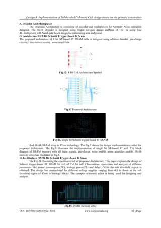
Fig 1: 6T SRAM Cell with A Word Line And Data Input And Output
III. 6t Sram Cell Operation
6T cells utilize differential write/Read operation, write operation will be performed whenever a change in the
transition on the inputs, during this wl is high and output is complementary to the input. Read operation will be
performed when there is no change in the transition of the input with WL is high [5]. A sense amplifier converts
the differential signal to a logic-level output. Then, at the end of the read cycle, the BLs returns to the positive
supply rail. During write,VWL is raised and the BLs are forced to either VDD (depending on the data),
overpowering the contents of the memory cell. During hold, VWL is held low and the BLs are left floating or
driven to VDD.
6T SRAM cell:
Fig 2: schematic representation of 6T SRAM
SRAM implementation represents in fig 2 of 6T bit cell of 6T, used with High Vth nMOS transistors for
reducing the Leakage Power [1]. The ratios of nMOS and pMOS are maintained with design considerations. To
drive transistors (M1,M4) should be stronger enough to access the Access transistors (M2,M5) to minimize the
disturbance in Read Mode. and in the Write Mode, Access transistors should be strong enough to operate
(M3,M6) for successful write operation. And Characteristics of 6T SRAM is represented as showed below
3. Design & Implementation of Subthreshold Memory Cell design based on the primary constraints
DOI: 10.9790/4200-0702015366 www.iosrjournals.org 55 | Page
Fig: 3 Represents the cell model of the bit cells in Synopsys tool. And hvt type of transistors is used to improve
the stability & performance. The schematic model of the SRAM cells designed in the 45nm technology the fig
and
Graph 3: DC Analysis
DC analysis of 6T SRAM is as shown in fig 3, and load will be exactly in the middle position of the
changing state characteristics curve, where from 1 to 0., The sizing of the transistors are as followed in table 1.
The output waveforms of different SRAM cell structures stated as at 45nm Technology.
4. Design & Implementation of Subthreshold Memory Cell design based on the primary constraints
DOI: 10.9790/4200-0702015366 www.iosrjournals.org 56 | Page
Table 1: Transistor sizing of the 6T SRAM cell
The limitation in 6T RAM is static Noise Margin [12]as showed in the graph 4..there should be maximum static
noise margin between the read and write operation, when changing the states from write to read.
Graph4 : Static Noise Margin of 6T SRAM cell
write operation when a logic and WL is high a data will be stored into SRAM, for a clock cycle ,and when the
logic the data will be remains in the output, once the logic is changed, data in the output will be shifted to another
logic.
IV. 8t Sram Cell
Two transistors were added to the 6T SRAM, read and write operations of Performance can be
completely separated. A separate read stack is controlled by a Read Word Line (RWL). The remaining 6T
portion of the cell is optimized [7] for writing operation, resulting in overall lower Vmin voltage.A Separated
data retention element and data output element means that there will be no correlation between the read SNM
Cell and l. Thus, an 8TSRAM design [7] contains a write assist in which a horizontally routed VDD line is
collapsed as showed in the fig 4.
Fig 4: 8T Subthreshold SRAM Cell
Fig 5: 8T schematic model of SRAM Cell
5. Design & Implementation of Subthreshold Memory Cell design based on the primary constraints
DOI: 10.9790/4200-0702015366 www.iosrjournals.org 57 | Page
The Fig.5 shows that 8T SRAM bit cell is designed with two sleep mode transistors, connected as pull
down mode transistors [7] to achieve low power design mode and to avoid the static noise margin. To write data
'1' into SRAM cell the WL is asserted and BL is made high and BLB is low. To write '0' BL is low and BLB
keeping high. The values of '0' or '1' can be stored at node Q and its complement at node QB. Reading the
stored value at node “Q” by precharging operation. After precharging the Bit Lines (BL=BLB=1) asserting the
WL and pulling down the one of the Bit Line low [8]. Data stability is increased with 8T.
9T SRAM Cell
The Fig.5a.demonstrates that 9T SRAM bit cell is to not only to reduce the leakage power also to
enhance data stability. The upper sub-circuit of the memory cell is essentially same as 6T SRAM cell. The two
write access transistors (M2, M5) are controlled by a write signal (WL). The lower sub-circuit of the cell is
composed of the bit line and access transistors (M7,M8), the read access transistor (M9). Operation of M7 and
M8 are controlled by the data stored in the cell. M9 is controlled by a separate read signal (RD) [5a.]in write
operation WL is asserted and making High and Read signal RD is maintained low. Transistors (M2,M5) are
turned ON. Then the data can be stored at node Q. and this data can be Read by asserting read signal RD to high
and WL to low. problem n 8T is indicated by occupying larger area and static noise margin is improved.[8][13].
The schematic diagram of the 9T SRAM cell, for CMOS technology, is shown in Fig.9. The upper sub circuit of
the 9T memory circuit is essentially a 6T SRAM cell with minimum sized devices(composed of M3, M4, M5,
M6, M1 and M2).The two write access transistors (M5 and M6) are controlled by a write signal ie word line
(WL). The data is stored within this upper memory sub-circuit. The lower sub circuit of the new cell is
composed of the bit-line access transistors (M7 and M8) and the read access transistor (M9). The operations of
M7 and M8 are controlled by the data stored in the cell. M9 is controlled by a separate read signal (RD)
[8][17].The 9T SRAM cell completely isolates the data from the bit lines during a read operation.
Fig.5a. 9T SRAM sub threshold Circuit
Table: 2 sizing of 9T SRAM
The length and widths of the 9T is as showed in the below table. Where the length is constant and width is
changing based on the ids and vds relationship[11].
Fig10: Schematic diagram of 9T SRAM cell
6. Design & Implementation of Subthreshold Memory Cell design based on the primary constraints
DOI: 10.9790/4200-0702015366 www.iosrjournals.org 58 | Page
Graph: 5. 9T SRAM characteristics at 400 mv
10 T SRAM Cell:
Fig.7. shows the schematic model of the 10T SRAM sub threshold logic cell[7][10]. Transistors are
equal to a 6T cell except the source of M1 and M2 tie to a virtual supply voltage rail of Vdd. Write admission
to the bit cell happens through the write contact transistors M5 and M6, Transistors from the write Bit lines,
WBLT and WBLC. Transistors M8 through M10 implement a buffer used for reading.
Fig.7. circuit diagram of the 10T SRAM cell.
Read access is a single-ended occurs on a separate bit line RBL, which is pre-charge to read access. The word
line read word line is also distinct from the write word line. One key Advantage is to separating the read & write
word lines and bit lines is that a memory using bit cell can have distinct read and write ports across the circuit.
And schematic model is as showed in fig 8.
Fig.8: schematic diagram of 10 TSRAM
Table: 3 Transistor sizing of the 10T SRAM cell Represents the sizes of length and widths of the Transistors
Configd as mentioned above
7. Design & Implementation of Subthreshold Memory Cell design based on the primary constraints
DOI: 10.9790/4200-0702015366 www.iosrjournals.org 59 | Page
Graph 4: Characteristics of 10T SRAM chcterstics are as shaowned above and are represented with read and
write lines
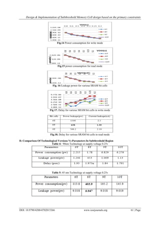
Vii A. Effect Of Temperature On Leakage Power And Current On Sram Bit Cells
All the circuits have been simulated using 45nm technology on Synopsys tool with supply voltage of different
ranging [15]. To make the neutral testing environment all the circuits has been simulated with the same input
patterns.
Graph 7. Leakage current variation of SRAM cell with Temperature
Characteristics of 7 and 8 shows comparative analysis of the circuits stated above at 45nm. The
simulation results reveal that 8T SRAM Cell at 45nm technology shows always best performance for the range
of power consumption, operating frequency and temperature
Fig .15 Leakage power variations of SRAM cells with Temperature
The leakage power and current of the SRAM cells for every 10 degrees rise or fall in temperature about
6-7% for 6T SRAM cell and 8T SRAM has 1-2% of current leakage and 0.1% of power leakage which shows
that 8T will be the better one amongst the other SRAM cells[15].
The power dissipation reduction in SRAMs is not only due to power supply voltage reduction, but also
to operating frequency and temperature. All the above figs depicts that SRAM cells at 45nm technology and 8T
SRAM cell at 45nm technology shows better performance for the range of frequency and temperature among all
the other design approaches[19] for SRAM cell. This paper tries to find out an efficient SRAM memory cell in
both the aspects power consumption and speed in terms of power delay product at different technologies[16].
The above table gives us a comparative study of the bit cells based on leakage and temperature at room
temperature i.e.,27degrees at the subthreshold voltage operation
B. Performance Metrics Of Power Consumption For Read And Write Operation, Leakage Power And
Delay At 90 Nm
These simulation results indicate the different SRAM bit cells. Analysis of different parameters of power
consumption, leakage power and delay under the sub threshold region. Measurements have been observed over
the of voltages from 0.8V down to the sub threshold region at 90 nm and 45 nm technologies. Comparison of
all the bit cells for parameters have been shown with respect to technologies.In 90nm technology the parameters
like power consumption, leakage power and delay are shown below (Fig9 to Fig13) power consumption and
8. Design & Implementation of Subthreshold Memory Cell design based on the primary constraints
DOI: 10.9790/4200-0702015366 www.iosrjournals.org 60 | Page
leakage power has been reducing by by reducing the supply voltage VDD from 0.8 to 0.2v where delay is
increasing.
Fig.9 power consumption for write mode
Fig.10. power consumption for read mode
Fig.11 leakage power for various SRAM bit cells
Fig.12 Delay for various SRAM bit cells in write operation
Fig.13. Delay for various SRAM bit cells in read operation
C. Performance Metrics Of Power Consumption For Read And Write Operation, Leakage Power And
Delay At 45 Nm
In 45nm technology it performs same as 45nm technology. But it showing the variation in delay as
shown in Fig.21,22,23. Power consumption and leakage power has been reducing by by reducing the supply
voltage VDD from 0.8 to 0.2v where delay is increasing.
9. Design & Implementation of Subthreshold Memory Cell design based on the primary constraints
DOI: 10.9790/4200-0702015366 www.iosrjournals.org 61 | Page
Fig.14 Power consumption for write mode
Fig.15 power consumption for read mode
Fig. 16 Leakage power for various SRAM bit cells
Fig 17. Delay for various SRAM bit cells in write mode
Fig.18. Delay for various SRAM bit cells in read mode
D. Comparison Of Technological Versions Vs Parameters In Subthreshold Region
Table 4: 90nm Technology at supply voltage 0.25v
Table 5: 45 nm Technology at supply voltage 0.25v
10. Design & Implementation of Subthreshold Memory Cell design based on the primary constraints
DOI: 10.9790/4200-0702015366 www.iosrjournals.org 62 | Page
Table 6: Comparative results of power and leakage current with different transistors of SRAM.
The paper indicates the comparative results of power consumption; leakage power and delay for both
read and write modes of operations in various technologies such as 90nm and 45nm of various SRAM Bit cells.
It has been observed that the leakage power is reduced by a factor 43% and 25% in consumption in 90 nm
technology, But in 45nm technology power consumption is reduced by a factor of 45 % and leakage power is
reduced by a factor of 21%. Delay is reduced in 9T SRAM Bit cell than the 6T/8T SRAM Bit cell. In
subthreshold region it is observed that the standard SRAM bit cell performance is given less priority than 8T
and 9T SRAM bit cells. The leakage power is reduced by using the high Vth nMOS transistors. Power
dissipation reduction in SRAMs is not only due to supply voltage, but also depends on the operating
frequency[22] and room temperature. All the above figs portray that SRAM cells at 45nm technology shows
better performance over a frequency and temperature among all the other design approaches.
This paper found out an efficient SRAM memory cell in both the aspects power consumption and speed in terms
of power delay product at different technologies. The above table gives us a comparative study of the bit cells
based on leakage at room temperature i.e., 27degrees at the subthreshold voltage operation
Proposed Sram Architecture
Schmitt Trigger-Based Sub-Vt 8T Static Ram Using 45 nm By Bit Interleaving Method
SRAM is a type of volatile semiconductor memory to store binary logic '1' and '0' bits. It uses bi stable latch
circuitry made of Transistors/MOSFETS to store each bit. An SRAM is designed to fill two needs to provide a
direct interface with the CPU at speeds not attainable by DRAMs and to replace DRAMs in systems that require
very low power consumption. The design requirement is such that PMOS OFF-state current should be more than
the pull-down nMOS transistor leakage current for maintaining data “1” reliably. With increasing process
variations and exponential dependence of the sub-threshold current on the threshold voltage, satisfying this
design requirement across different process, voltage, and temperature (PVT) conditions may be challenging.[13]
Proposed Architecture is designed using Schmitt trigger-based 8T SRAM bit cell illustrated in Fig.[7]. It is
similar to the standard 6T SRAM cell, however it is used High-Vth nMOS in this design [7]. Two sleep
transistors are used in pull down path to minimize the leakage power [15]. These Transistors used for self-
correcting feedback to achieve stable operation. This cell also reduces dynamic power in active mode.
A. Schmitt Trigger-Based 8t Sram
nMOS should win the ratio fight with pMOS. If we want to write data'1' making the WL=1 and one of the bit
line keeping High BL(or)BLB=1 and other is 0.Then the value is been written as '1' at node 'Q' and its
complement at node 'QB'.
B. Write Operation
In the write operation, WL is enabled to activate the access transistors for data transfer . The proper write
operation can be done successfully by consideration of ratio(W/L) of nMOS and pMOS[8]. In sizing of transistors
in SRAM bit cell.
Fig.9. The Schematic of a single cell write operation
11. Design & Implementation of Subthreshold Memory Cell design based on the primary constraints
DOI: 10.9790/4200-0702015366 www.iosrjournals.org 63 | Page
Fig.19. Read and write operations of SNM of the proposed SRAM
C. Read Operation
In the read operation, BL and BLB are precharged to initial condition and WL is enabled then one of
the Bit line (BL/BLB) is enabling to low. The read value can be observed by enabling the Sense Amplifier. The
written data can be stored at node 'Q' and its complement at 'QB' in standby mode. This data can be withheld at
the node till the read operation being accessed. The leakage has been minimized by using the sleep mode
transistors in pull down path and effectively read by acting as feedback transistors.
D. Sense Amplifier
The voltage mode sense amplifier is used for designing. This is the Enhanced Positive Feedback sense
amplifier is using to operate the read operation effectively and it can reduces the bit line capacitances by
decoupling the nMOS transistors in design shown. The written data can be enhanced effectively h. This design
operated at 0.4V and power dissipation is 942.2pW Units. When SE=1.Sense ModeSE=0,Standby Mode
operation.
Fig.10. Enhanced Positive Feedback Sense Amplifier
E. Data Write Circuit
Write operation into the memory cell can be done only when the write enable ON. This enable
operation can be easily understood by the following circuit Fig.10. Write operation into the memory cell can be
done only when the write enable ON. This enable operation can be easily understood by the following circuit.
The design being operate at0.4V and observed delay and power 4.79nS,1.38nW respectively
Fig.11. Data Write Circuit
12. Design & Implementation of Subthreshold Memory Cell design based on the primary constraints
DOI: 10.9790/4200-0702015366 www.iosrjournals.org 64 | Page
F. Decoder And Multiplexer
The proposed Architecture is consisting of decoder and multiplexers for Memory Array operation
designed. The 4to16 Decoder is designed using 4input nor-gate design andMux of 16x1 is using four
4x1multiplxers with Nand-gate based design for minimizing area and power.
G. Architecture Of 8 Bit Schmitt Trigger-Based 8t Sram
The proposed architecture of 8 bit ST-based 8T SRAM cells is designed using address decoder, pre-charge
circuitry, data write circuitry, sense amplifiers
Fig.12: 8 Bit Cell Architecture Symbol
Fig.13 Proposed Architecture
Fig:14. single bit Schmitt trigger-based 8T SRAM
And 16x16 SRAM array in 45nm technology. The Fig.5 shows the design implementation symbol for
proposed architecture. The Fig.8 illustrates the implementation of single bit ST-based 8T cell. The block
diagram of SRAM memory with all input signals, pre-charge, write enable, sense amplifier enable, 16x16
memory array has illustrated in Fig.8.
H.Architecture Of 256 Bit Schmitt Trigger-Based 8t Sram
The Fig.31 illustrating the operation result of proposed Architecture. This paper explores the design of
Schmitt trigger-based 8T SRAM bit cell of 256 bit cell. Observations, operations and analysis of different
parameters like power consumption(PC), leakage power(PL) and delay (DL)in the sub threshold region is
obtained. The design has manipulated for different voltage supplies varying from 0.8 to down in the sub
threshold region of 45nm technology library. The synopsis schematic editor is being used for designing and
analysis.
Fig.15. 256Bit memory array
13. Design & Implementation of Subthreshold Memory Cell design based on the primary constraints
DOI: 10.9790/4200-0702015366 www.iosrjournals.org 65 | Page
Table.7: operation result of SRAM Cell
VDD Single bit 16bit 256bit
Power
Consumption(PW)
12.765nW 317.9nW 474.6nW
Leakage Power(PL) 0.497nW 4.74nW 7.98nW
Delay 114.6ns 156.4ns 168.9ns
Fig.21. Performance characteristics of operation
V. Conclusion
The paper gives a broad idea about designing of memory cell using number of transistors with different
technologies and operating at different subthreshold regions, and has been shown that the comparative results
of power consumption(PC), leakage power(PL) and delay (DL)for both read and write modes of operations in
various technologies such as 90nm various SRAM Bit cells. Its has observed that the leakage power is reduced
by a factor 43% and 25% in consumption in 90 nm technology using 8T transistor modeling.
And in 45nm Technology power consumption is reduced by a factor of 45 % and leakage power is
reduced by a factor of 21%. Delay is reduced in 9T SRAM Bit cell than 6T/8T SRAM bit cell. But in
subthreshold region it is observed that the standard SRAM bit cell performance is given less priority than 8T
and 9T SRAM bit cells. The leakage power is reduced by using the high Vth nMOS transistors.
References
[1] SRAM cell with improved stability and reduced leakage current for subthreshold region of operation” by P. Sreelakshmi, K. S. Pande
and N. S. Murty In 2015 IEEE International Conference on Computational Intelligence and Computing Research (ICCIC), Madurai,
2015, pp. 1-5.doi: 10.1109/ICCIC.2015.7435750.
[2] David J. Comer, Senior Member, IEEE, and Donald T. Comer"Operation of Analog MOS Circuits in the Weak or Moderate Inversion
Region" IEEE TRANSACTIONS ON EDUCATION, VOL. 47, NO. 4, NOVEMBER 2004.
[3]. "Low-power 9T subthreshold SRAM cell with single-ended write scheme, By A. Sinha, V. Kumar and A. Islam, " 2015
AnnualIEEE India Conference (INDICON), New Delhi, 2015, pp. 1-6.doi: 10.1109/INDICON.2015.7443137.[10]. "Analysis of
SRAM cell designs for low power applications, By C. K. Sharma and R. Chandel, " Convergence of Technology (I2CT), 2014
International Conference for, Pune, 2014, pp. 1-4.doi: 10.1109/I2CT.2014.7092157
[3] Alice Wang Benton H. Calhoun Anantha P. Chandrakasan "Sub-threshold Design for Ultra Low-Power Systems"SERIES ON
INTEGRATED CIRCUITS AND SYSTEMS
[4] Chang, L. Montoye, R.K. Nakamura, Y.Batson, K.A.Eickemeyer, R.J.Dennard, R.H. Haensch,W.Jamsek, D, “An 8T-SRAM for
variability tolerance and low-voltage operation in highperformancecaches”, Solid-State Circuits, IEEE Journal vol. 43, April 2008,
Issue 4, pp-956-963.
[5] NavidAzizi, FaridN.Najm. An asymmetricSRAM cell to lower gate leakage. In proceedingsof International Symposium on Quality
ElectronicDesign, pp.534-539, March 2004
[6] Ravi Kumar. K. I, Vijayalaxmi. C. Kalal, Rajani. H. P, Dr. S. Y. Kulkarni"Design and Verification of Low Power 64bit SRAM
System using 8T SRAM:Back-End Approach" International Journal of Engineering and Innovative Technology (IJEIT) Volume 1,
Issue 6, June 2012.
[7] A new low-leakage T-Gate based 8T SRAM cell with improved write-ability in 90nm CMOS technology, G. Pasandi, E. Qasemi and
S. M. Fakhraie, " 2014 22nd Iranian Conference on Electrical Engineering (ICEE), Tehran,2014,pp.382-386.doi-
10.1109/IranianCEE.2014.6999569
[8] Chang, L. Montoye, R.K. Nakamura, Y.Batson, K.A.Eickemeyer, R.J.Dennard, R.H. Haensch,W.Jamsek, D, “An 8T-SRAM for
variability tolerance and low-voltage operation in highperformancecaches”, Solid-State Circuits, IEEE Journal vol. 43, April 2008,
Issue 4, pp-956-963.
[9] Wei-Bin Yang, Chi-Hsiung Wang, I-Ting Chuo, Huang- Hsuan Hsu" A 300 mV 10 MHz 4 kb10T Subthreshold SRAM for
Ultralow-Power Application" 2012 IEEE International Symposium on Intelligent Signal Processing and Communication Systems
(ISPACS 2012) November 4-7, 2012.
[10] Zhiyu Liu and Volkan Kursun "Characterization of a Novel Nine-Transistor sram cell" ieee transactions on very large scale
integration (vlsi) systems, vol. 16, no. 4, april 2008
[11] Koichi Takeda , “A read static noise margin free SRAM cell for low Vdd and high speed applications”, Solid-State Circuits, IEEE
Journal vol. 41, Jan.2006, Issue 1, pp.113-121.
[12] Zhiyu Liu, Volkan Kursun, “ Characterization of a novel nine transistor SRAM cell”, IEEE Transactions on Very Large Scale
Integration Systems,vol.46, Issue 4,April 2008.pp-488-492.
14. Design & Implementation of Subthreshold Memory Cell design based on the primary constraints
DOI: 10.9790/4200-0702015366 www.iosrjournals.org 66 | Page
[13] A Feasibility Study of Subthreshold SRAM Across Technology Generations” ArijitRaychowdhury, SaibalMukhopadhyay, and
Kaushik Roy Dept. of ECE, Purdue University, West Lafayette, IN-47907 <araycho, sm, kaushik>@ecn.purdue.edu.
[14] Jawar Singh, DhirajK.Pradhan,” A single ended 6T SRAM cell design for ultra low voltageapplications”, IEICE Electronic Express,
2008, pp-750-755.
[15] "Analysis of SRAM cell designs for low power applications," by C. K. Sharma and R. Chandel, Convergence of Technology
(I2CT), 2014 International Conference for, Pune, 2014, pp. 1-4.doi: 10.1109/I2CT.2014.7092157
[16] A 1kb 9T subthreshold SRAM with bit-interleaving scheme in 65nm CMOS BY M. H. Chang, Y. T. Chiu, S. L. Lai and W. Hwang,
Low Power Electronics and Design (ISLPED) 2011 International Symposium on, Fukuoka, 2011, pp. 291-296.doi:
10.1109/ISLPED.2011.5993652
[17] B. Zhai, et al., “Analysis and Mitigation of Variability in Subthreshold Design,” ISLPED, pp. 20-25, 2005.
[18] “Analyzing and Modeling Process Balance for Sub-threshold Circuit Design” Joseph F. Ryan, Jiajing Wang, and Benton H. Calhoun
Department of Electrical and Computer Engineering University of Virginia, Charlottesville, Virginia 22904
[19] A. Wang, B. Calhoun, and A. Chandrakasan, “Sub-threshold Design for Ultra Low-Power Systems”, Springer, 2006.[15] “A 160 mV
Robust Schmitt Trigger Based Subthreshold SRAM” Jaydeep P. Kulkarni, Student Member, IEEE, Keejong Kim, and Kaushik Roy,
Fellow, IEEE.
[20] H.Soeleman and K. Roy,” Ultra-low power digital subthreshold logic circuits,” International Symposium on Low Power Electronics
and Design (ISLPED 99), pp. 94–96, San Diego, California, USA, July 1999.
[21] “An Ultra-Low-Power Memory With a Subthreshold Power Supply Voltage” Jinhui Chen, Student Member, IEEE, Lawrence T.
Clark, Senior Member, IEEE, and Tai-Hua Chen, Student Member, IEEE