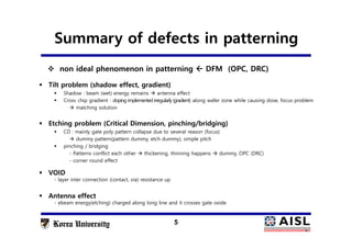
The document is a comprehensive guide focused on high-speed CMOS IC layout techniques, including lithography defects, layout techniques, and high-speed layout guidelines. It addresses common issues in semiconductor design such as matching, loading, reliability, and offers solutions to mitigate lithography-related errors. The content is structured into three main parts: lithography defects and their prevention, layout optimization techniques, and a checklist for high-speed design considerations.
![6
Figure 2: pinching and bridging during manufactureFigure 1: Process variation band.
Figure 4: Bridging failure.Figure 3: pinching failure.
process variability bands / bridging, pinching
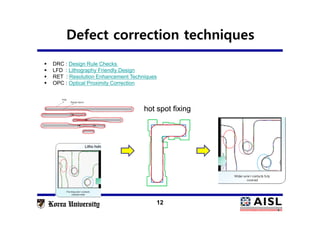
hotspot (Critical Dimension) Error (next page)
pattern defect examples [1]](https://image.slidesharecdn.com/nanometerlayouthandbookathighspeeddesign-170615123243/85/Nanometer-layout-handbook-at-high-speed-design-6-320.jpg)
![7
gate-poly defect (Critical Dimension) example
thickening, thinning, pinching and ... all GP defects
closely related with circuit performance degradation.
thickening, thinning, pinching and ... all GP defects
closely related with circuit performance degradation.
gate-poly pattern defects (CD) [2]](https://image.slidesharecdn.com/nanometerlayouthandbookathighspeeddesign-170615123243/85/Nanometer-layout-handbook-at-high-speed-design-7-320.jpg)
![9
charge dissipation
@active on the bulk
charge dissipation
@active on the bulk
++++
++++
++++
Plasma damage - Antenna effect [4]
e-beam energy charged by plasma
along antennas (long metal lines)
at high resistance / capacitance burst out.
e-beam energy charged by plasma
along antennas (long metal lines)
at high resistance / capacitance burst out.
+++
+
++
e-beam
(by plasma)
energy charged along
surface of shadow region](https://image.slidesharecdn.com/nanometerlayouthandbookathighspeeddesign-170615123243/85/Nanometer-layout-handbook-at-high-speed-design-9-320.jpg)
![10
. charging
. damage
Qbd : 1~100 coulomb/cm2
(breakdown chage )
MOS transistor with positive bias on the gate
electrons that can hop over or tunnel through the oxide-
semiconductor barrier can travel through the oxide.
Electric fields are high, and the electrons can gather
energy and do damage (break bonds) as they proceed.
plasma damage [3]](https://image.slidesharecdn.com/nanometerlayouthandbookathighspeeddesign-170615123243/85/Nanometer-layout-handbook-at-high-speed-design-10-320.jpg)
![11
From Automated hot-spot fixing system applied to the metal layers of 65-nm logic devices
@ Journal of Micro/Nanolithography, MEMS, and MOEMS
Defect correction method [5]](https://image.slidesharecdn.com/nanometerlayouthandbookathighspeeddesign-170615123243/85/Nanometer-layout-handbook-at-high-speed-design-11-320.jpg)
![Parasitic loading effects [6]
18
phase delay θd and gain |G|
3) Capacitance Cp in Fig. 3(b) represents the parasitic capacitance Cpw with a wire line in Fig 3(a),
and also includes the input parasitic capacitances of the following stage in Fig. 2.
4) Furthermore, the parasitic resistance Rp with the wireline is connected to the output node.
Gain degraded by α (Cp, Rp)](https://image.slidesharecdn.com/nanometerlayouthandbookathighspeeddesign-170615123243/85/Nanometer-layout-handbook-at-high-speed-design-18-320.jpg)
![21
• shift placed (differential pair shifted)
• Process variations are averaged among transistors (good dc condition)
• good matching technique for dc condition
• total drain area uneven between M1 and M2. drain capacitance uneven
(not desirable ac conditions: capacitance, other parameters may not be equal)
• A more robust approach is needed (Use dummies if needed !!)
Inter-digitized Layout [7]
M1:KP1+KP4+KP5+KP8 (Avg=4.5)
M2:KP2+KP3+KP6+KP7 (Avg=4.5)
Samuel Palermo
concept and example of inter-digitized layout
good for DC conditioned schematic](https://image.slidesharecdn.com/nanometerlayouthandbookathighspeeddesign-170615123243/85/Nanometer-layout-handbook-at-high-speed-design-21-320.jpg)
![22
• Each transistor is split in four equal parts interleaved in two by two’s.
So that for one pair of pieces of the same transistor we have currents flowing in opposite direction.
• Transistors have the same source and drain area and perimeters, but this topology is more susceptible
to gradients (not common centroid)
Inter-digitized Layout (2) [7]
improved Inter-digitized Layout – capacitive matched !
shift placed (not mirrored) gradient not cancelled, but good for DC/AC conditions
Samuel Palermo](https://image.slidesharecdn.com/nanometerlayouthandbookathighspeeddesign-170615123243/85/Nanometer-layout-handbook-at-high-speed-design-22-320.jpg)
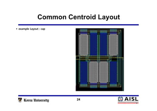
![23
Common Centroid Layout [7]
• split in even for parallel connection mirror placed (differential pair mirrored)
• good for RF application
(less effective of crosstalk mismatch, junction capacitance mismatch)
M1M2M2M1M1M2M2M1
M1M2M2M1M1M2M2M1
M2M1M1M2M2M1M1M2
Samuel Palermo
Common Centroid Layout
Inter-digitized Layout](https://image.slidesharecdn.com/nanometerlayouthandbookathighspeeddesign-170615123243/85/Nanometer-layout-handbook-at-high-speed-design-23-320.jpg)
![capacitance – loading [9]
29
Dan Clein
Fringe cap : self loading cap
Process gets narrow, metal stacks
higher Fringe cap higher
Fringe cap : self loading cap
Process gets narrow, metal stacks
higher Fringe cap higher Coupling cap : planar, 3D Coupling cap : planar, 3D
Coupling cap with
Coupled with metals every
where with substrate coupling
effects
Coupling cap with
Coupled with metals every
where with substrate coupling
effects
Coupling cases](https://image.slidesharecdn.com/nanometerlayouthandbookathighspeeddesign-170615123243/85/Nanometer-layout-handbook-at-high-speed-design-29-320.jpg)
![30
capacitance – coupling (Crosstalk) [9]
Bottom capacitance Cb
mutual capacitances Cm
Top capacitances Ct added
Dan Clein
Coupling loading through parasitic capacitance of long running metal lines affects seriously on
signal normally tR, tF
It happens not only planar but also 3D. The Tops and Bottoms
M1](https://image.slidesharecdn.com/nanometerlayouthandbookathighspeeddesign-170615123243/85/Nanometer-layout-handbook-at-high-speed-design-30-320.jpg)
![capacitance – signal line shield [9]
31
< Differential pair twisting to reduce signal coupling (PCB technique) >
effect of coupling - DC signal shield effect of coupling - DC signal shield
aggressor
victim
aggressor
victim
tPD (delayed)
tPD (normal)
XX : aggressor
. twisted line : coupling noise canceled with differential pair common mode
. shield with vss line.
XX : aggressor
. twisted line : coupling noise canceled with differential pair common mode
. shield with vss line.
Coupling effects : aggressor affects on victim.
Critical signal line could be shielded with static
level signal. This technique will eliminate the
worse-case coupling scenario
Coupling effects : aggressor affects on victim.
Critical signal line could be shielded with static
level signal. This technique will eliminate the
worse-case coupling scenario
effect of coupling - diff pair twist shield effect of coupling - diff pair twist shield
case 1 case 2
. twisted line
. differential pair
. twisted line
. differential pair
XX : aggressor
1
2
1
2
. twisted line, differential pair
. vss shield
. twisted line, differential pair
. vss shield
Dan Clein
Coupling : Victim and Aggressor cases](https://image.slidesharecdn.com/nanometerlayouthandbookathighspeeddesign-170615123243/85/Nanometer-layout-handbook-at-high-speed-design-31-320.jpg)
![capacitance – Vref line shield [9]
33
< Shielding option examples in two-metal process >
shield form all way if it needs shield form all way if it needs
Cc_lower
Cc_upper
Vref line
VSS
VSS
• case : isolating the signal from influences on the same layer both sides
• case : isolating the signal from influences on the same layer and upper/lower layers
• case : isolating the signal from influences on the same layer both sides
• case : isolating the signal from influences on the same layer and upper/lower layers
• Voltage reference level is critical to comparator and buffer.
• Reference level could be corrupted by signal line toggling.
• So keep reference line safe as isolate it from signal lines everywhere
• Voltage reference level is critical to comparator and buffer.
• Reference level could be corrupted by signal line toggling.
• So keep reference line safe as isolate it from signal lines everywhere
Dan Clein
Shield : important signal / reference line shielding cases](https://image.slidesharecdn.com/nanometerlayouthandbookathighspeeddesign-170615123243/85/Nanometer-layout-handbook-at-high-speed-design-33-320.jpg)
![34
capacitance – Vref line shield [9]
< Shielding option examples in three-metal process >
Dan Clein](https://image.slidesharecdn.com/nanometerlayouthandbookathighspeeddesign-170615123243/85/Nanometer-layout-handbook-at-high-speed-design-34-320.jpg)
![35
Resistor – (symmetry) [9]
< resistor shielding >< interlaced resistor shielding >
Dan Clein
Shield : line resistor shielding cases
Line resistor is used for small and simple resistor
Line resistor is also used for skew (tPD) matching. This technique is good for multi bit skew aligning.
Line resistor is used for small and simple resistor
Line resistor is also used for skew (tPD) matching. This technique is good for multi bit skew aligning.
A2
A1
A1 A2
A2 is delayed to A1 RC delay added to A1](https://image.slidesharecdn.com/nanometerlayouthandbookathighspeeddesign-170615123243/85/Nanometer-layout-handbook-at-high-speed-design-35-320.jpg)
![36
Balanced NAND – input unbalanced [9]Dan Clein
in2
in1
out
Balanced NAND
One of inputs must be closer (or faster) to output than the other.
To prevent unbalanced path, split NMOS fingers and attach all input TRs to output.
In1 is faster than in2
< Conventional NAND > < Balanced NAND >
in2
in1
out
In1 is slower as in2 is](https://image.slidesharecdn.com/nanometerlayouthandbookathighspeeddesign-170615123243/85/Nanometer-layout-handbook-at-high-speed-design-36-320.jpg)
![Balanced layout [9]
37
The schematic shown on the right side of Figure 7.20 shows exactly how the schematic is defined for Example 3. Many LVS
layout verification tools have algorithms to recognize NAND gates within the layout. The layout NAND shown in Example 3 is
not often recognized as a NAND and creates discrepancies when compared to a regular schematic NAND. The reason is
that the order of the series connections within the NAND is reversed. Functionally, they are equivalent and in fact balanced.
In this case the schematic must be altered to reflect the correct connectivity in order for the LVS to pass.
Balancing circuits is not always as straightforward. Balancing series devices is more difficult when dealing with more than
two transistors connected in series. Figure 7.21 shows an example of three series gates to illustrate this concept further.
In order to balance the series connections, each input is connected to a transistor in each of the three positions: close to
out, center, and close to power. This is only possible if there are three parallel series chains; therefore, introducing
balancing to a layout may incur significant overhead.
Dan Clein](https://image.slidesharecdn.com/nanometerlayouthandbookathighspeeddesign-170615123243/85/Nanometer-layout-handbook-at-high-speed-design-37-320.jpg)