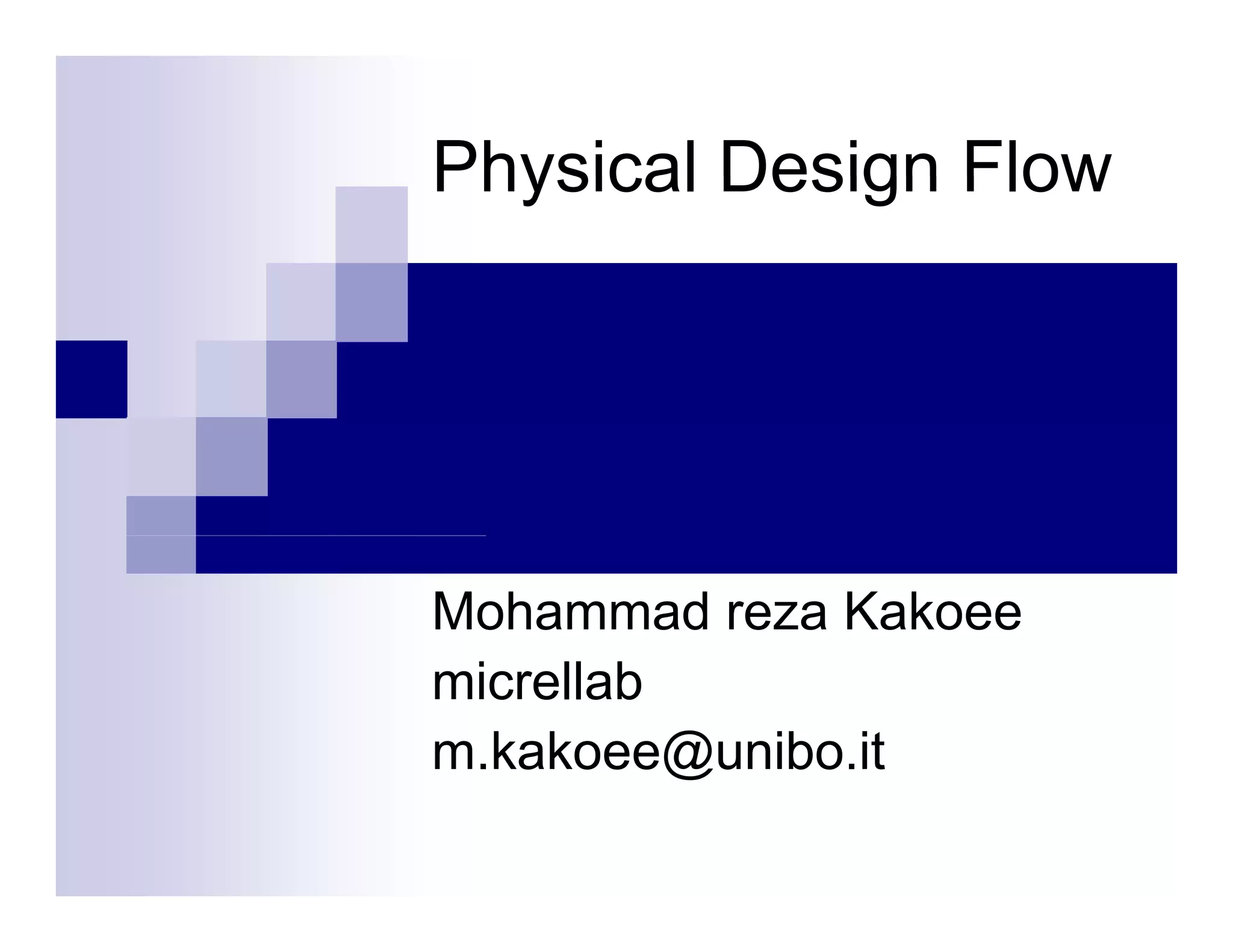
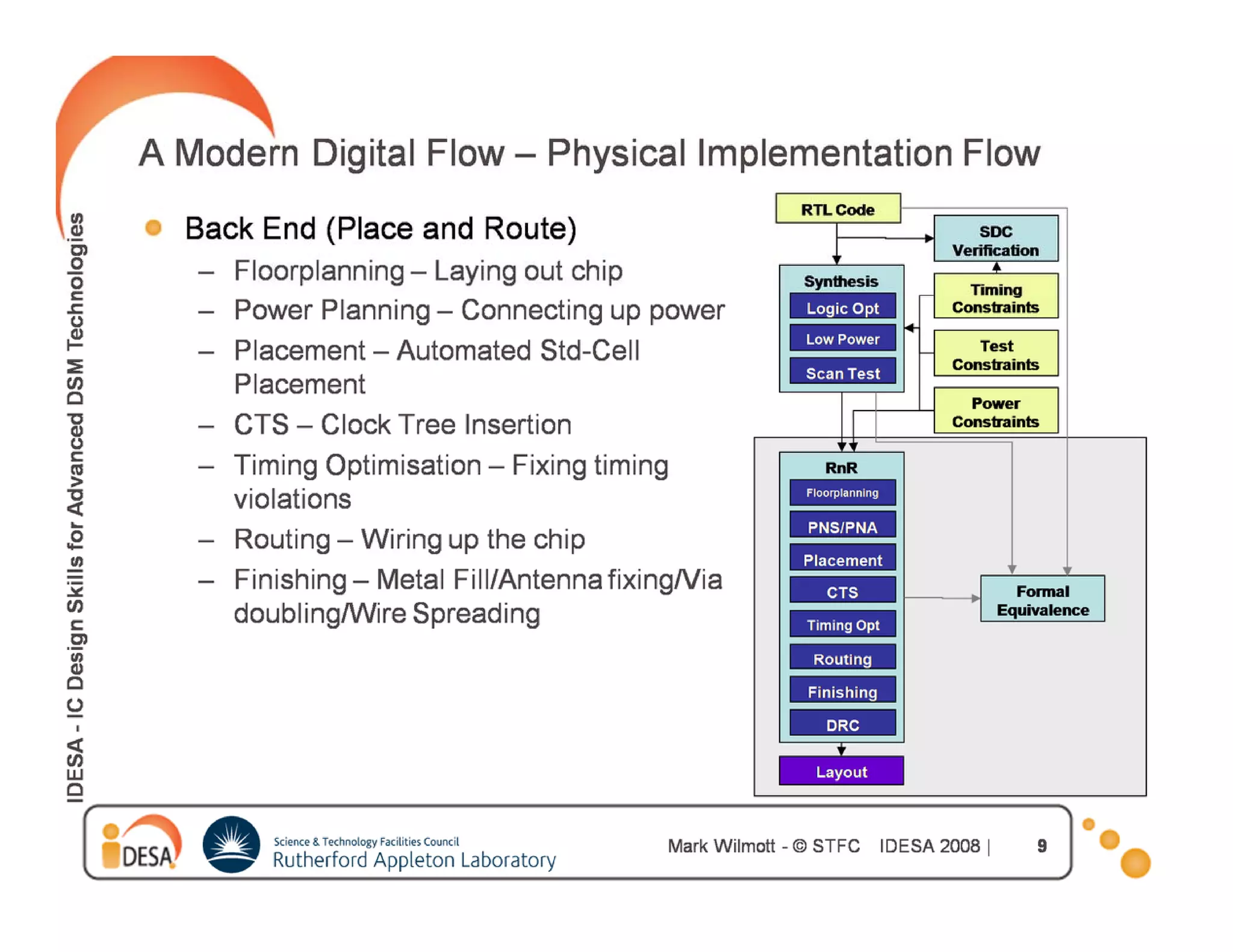
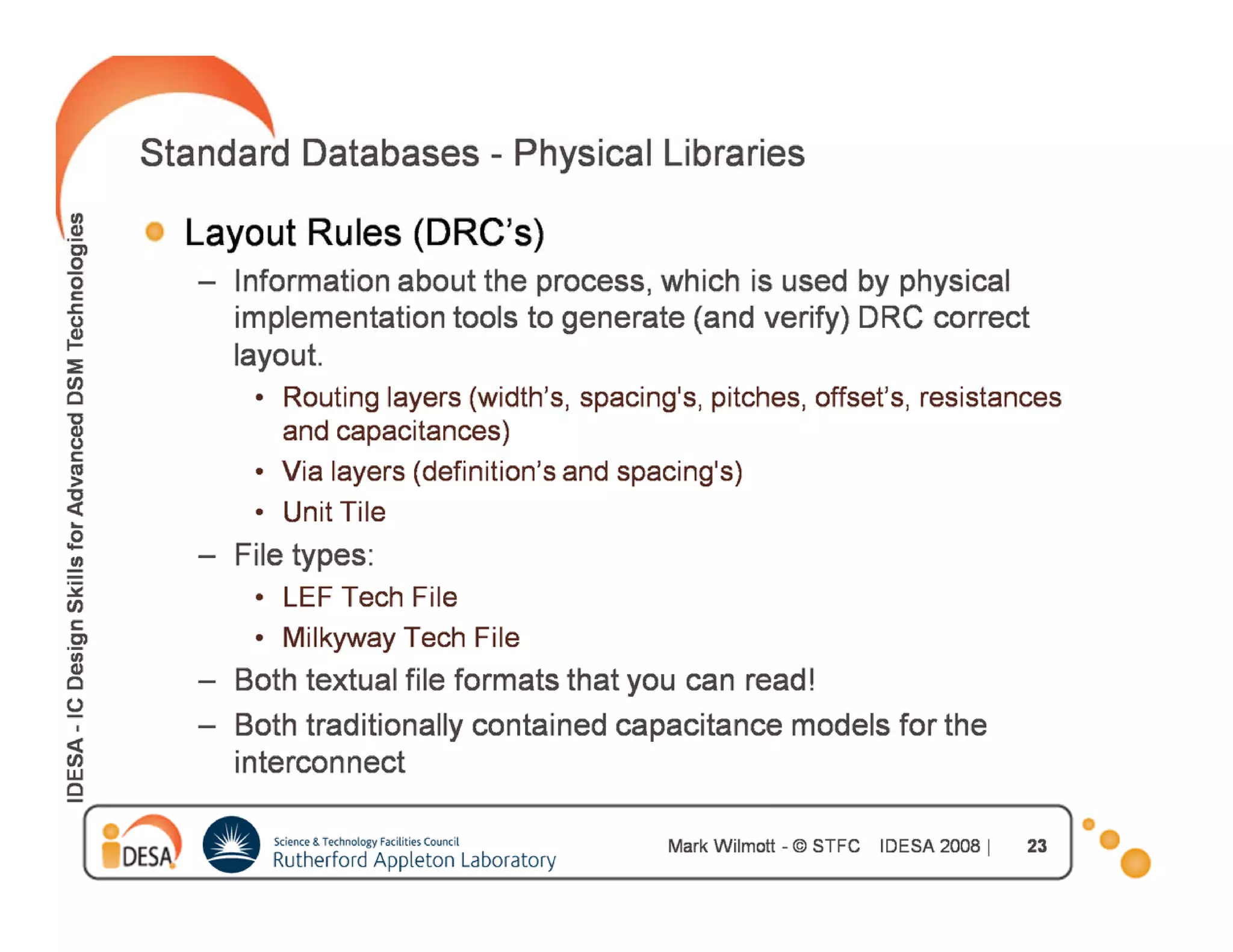
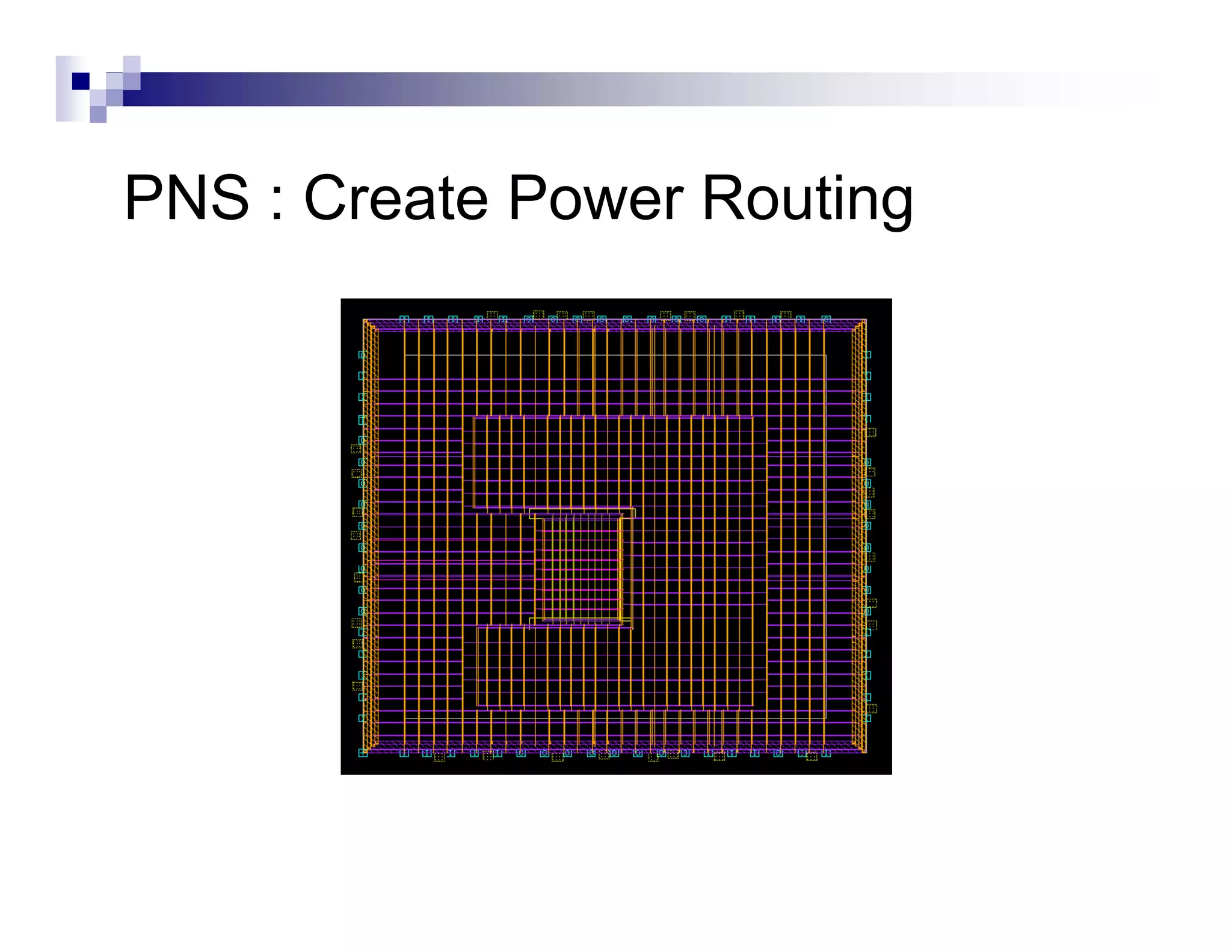
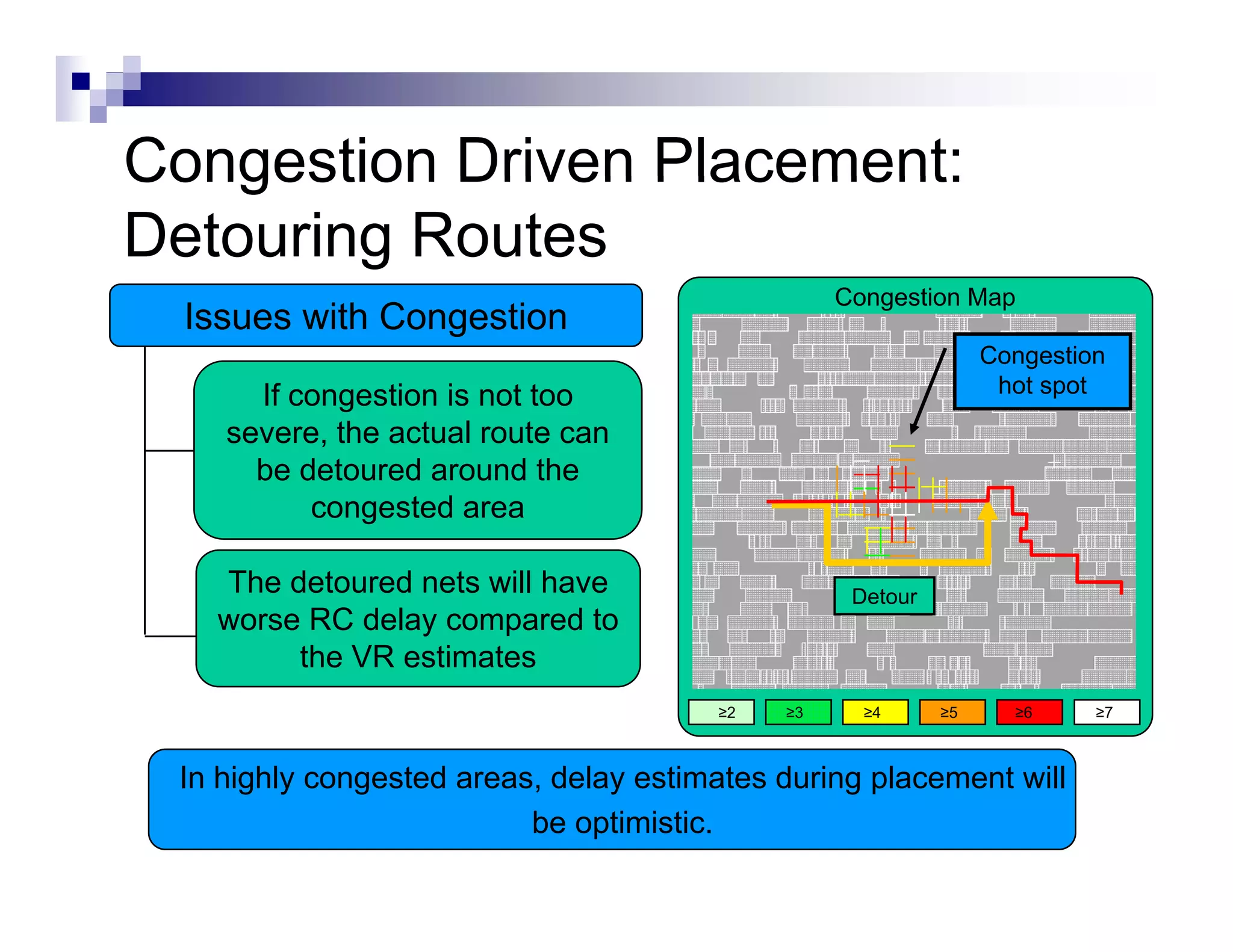
![Initialize Floorplan
Define globals (VDD1,VDD2,GND1,….)
Define
D fi core area : ( ll + utilization f
(cells ili i factor)
)
IO [
[Analog] macro
g]
core
core
IO
Shape can be implied by a macro
Place IO (fixed, equidistant,..)
Take macro’s and power domains into
account already](https://image.slidesharecdn.com/hwkakoee2-130205113011-phpapp01/75/VLSI-Physical-Design-Tool-Terminalogy-22-2048.jpg)
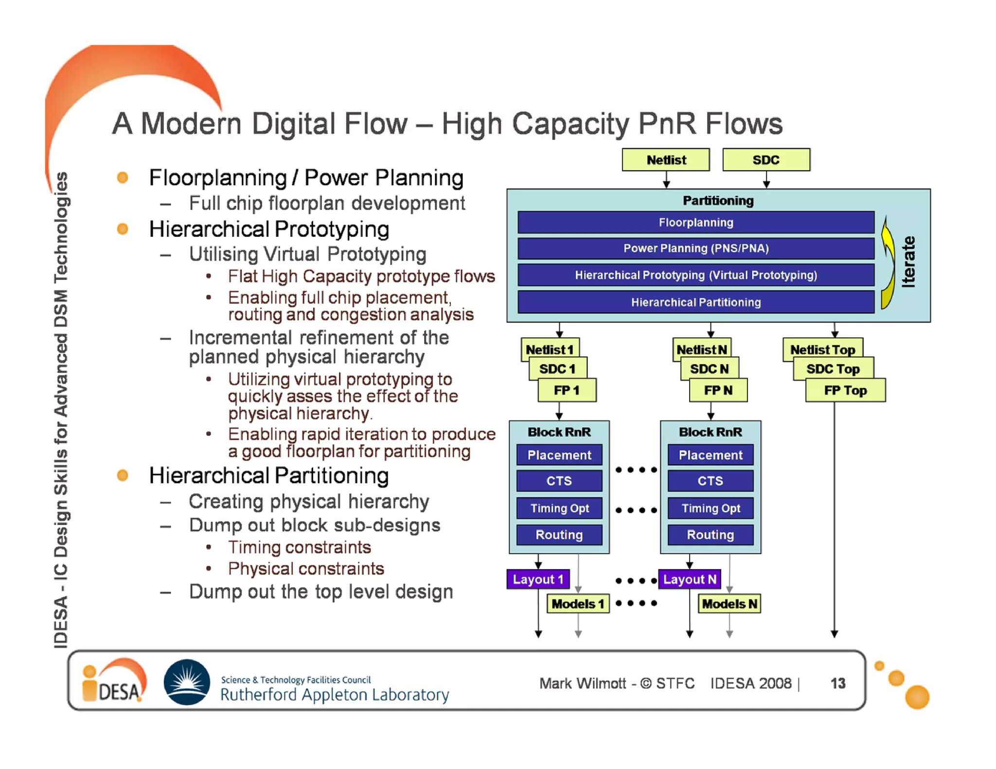
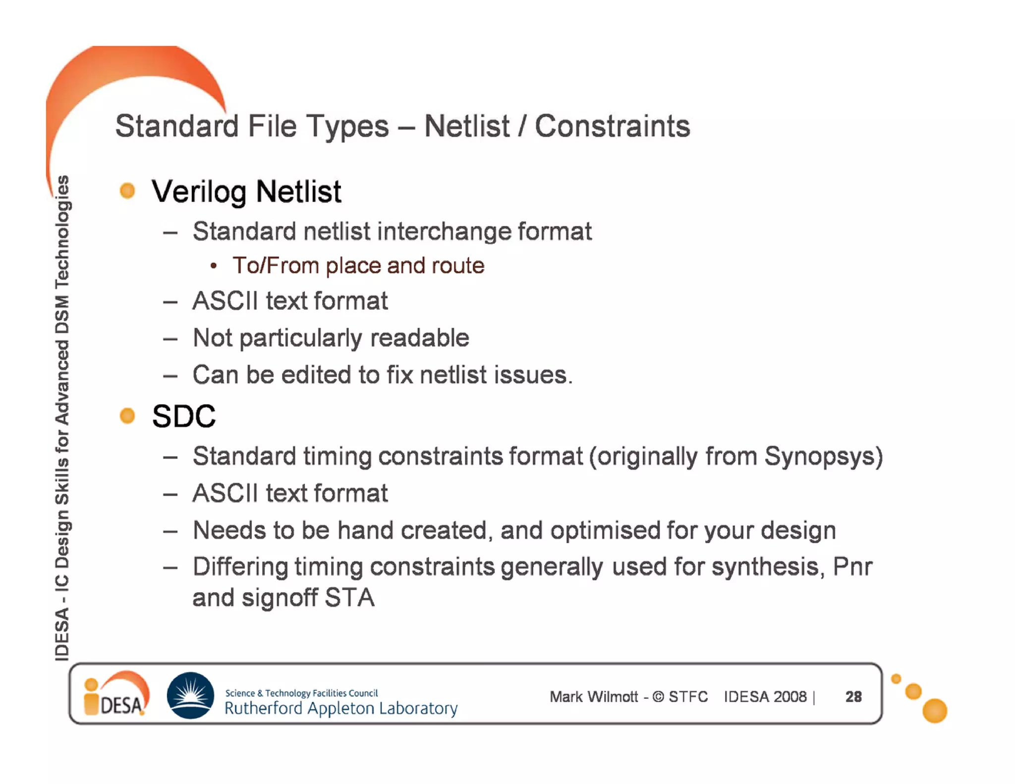
![Hierarchical Design : Timing
Budgeting
Chip level constraints must be mapped correctly to block
level constraints
The d i
Th design must b placed, t i l routed and h
t be l d trial t d d have pinsi
assigned before running budgeting
Block level constraints will be assigned input or output
delays on I/O ports based off of the estimated timing
slack.
IN1 set_input_delay 1.5 get port
set input delay 1 5 [ get_port IN1 ]
1.5ns
Block Boundary](https://image.slidesharecdn.com/hwkakoee2-130205113011-phpapp01/75/VLSI-Physical-Design-Tool-Terminalogy-28-2048.jpg)
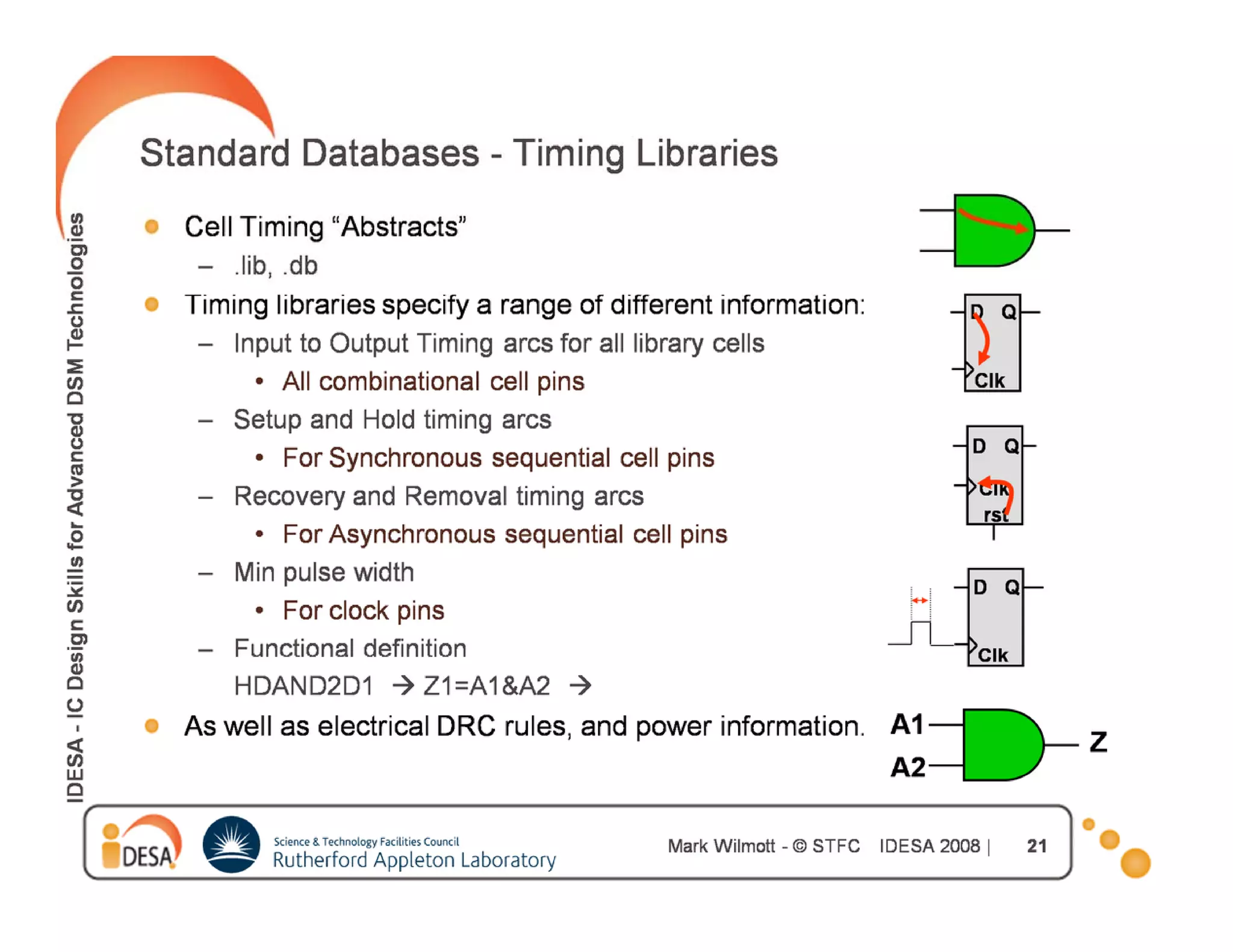
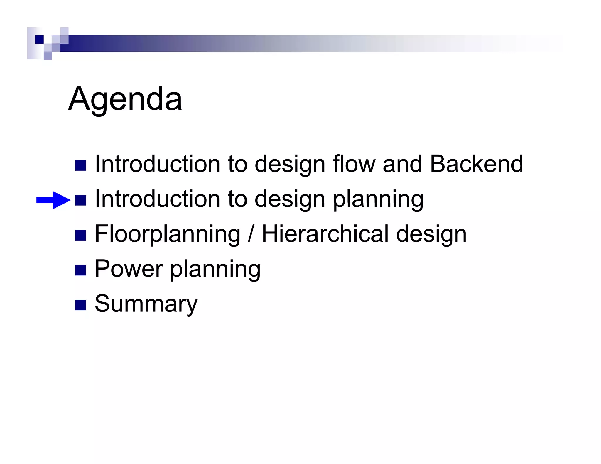
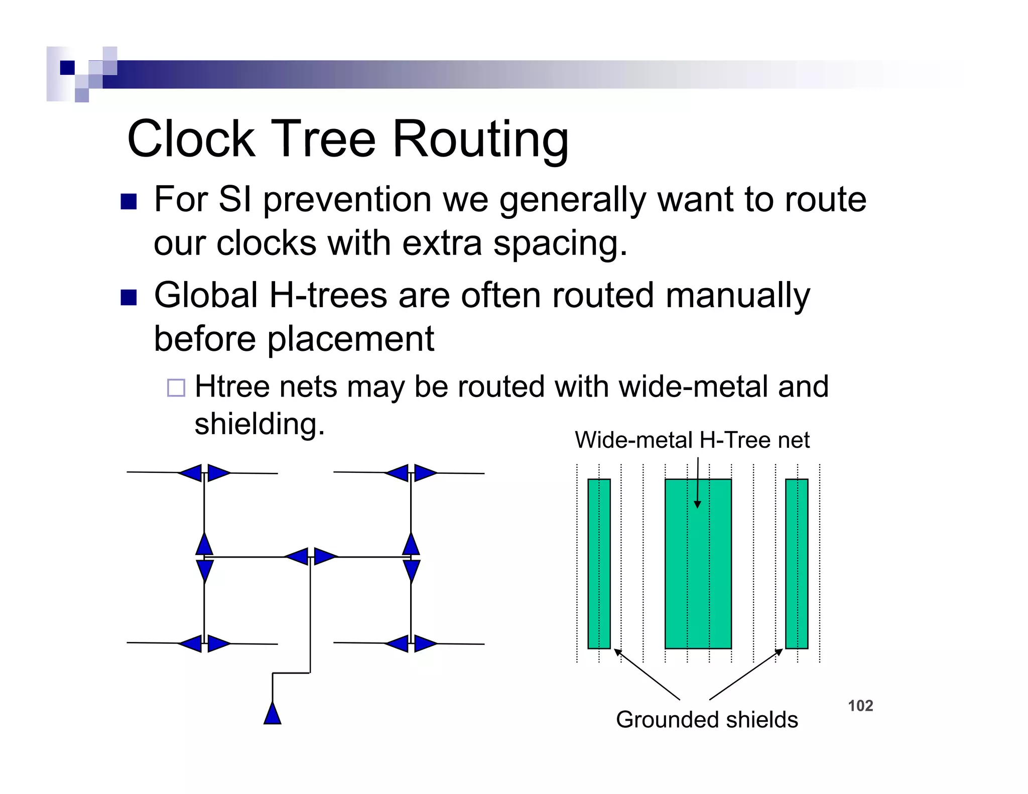
![CTS : Goals
Meeting the clock tree design rule
constraints
Constraints are upper
Maximum transition delay
bound goals. If constraints
Maximum load capacitance are not met, violations will
t t i l ti ill
Maximum fanout be reported.
[
[Maximum buffer levels]
]
defaults
Meeting the clock tree targets
Maximum skew Highest priority
Min/Max insertion delay (latency)
77](https://image.slidesharecdn.com/hwkakoee2-130205113011-phpapp01/75/VLSI-Physical-Design-Tool-Terminalogy-77-2048.jpg)
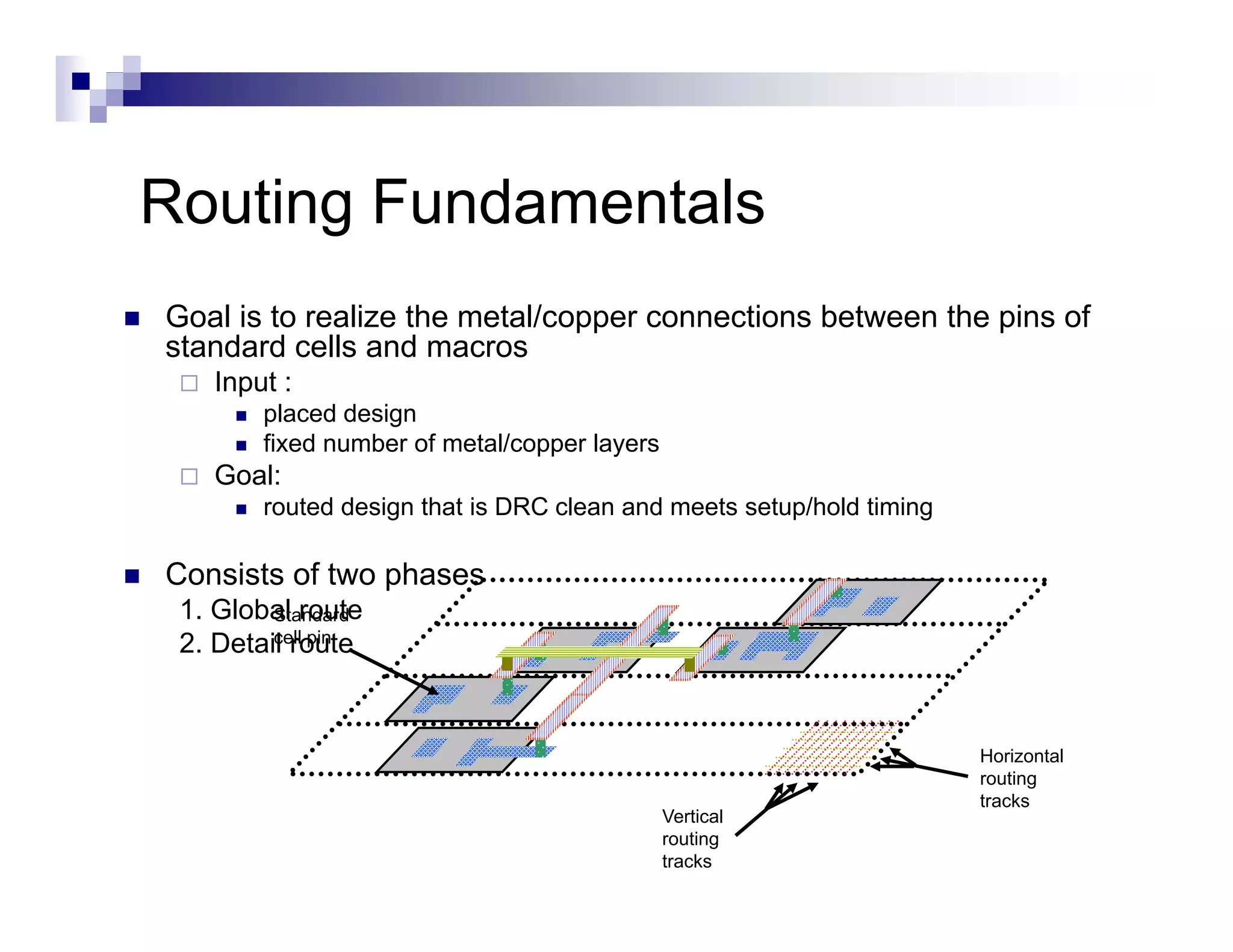

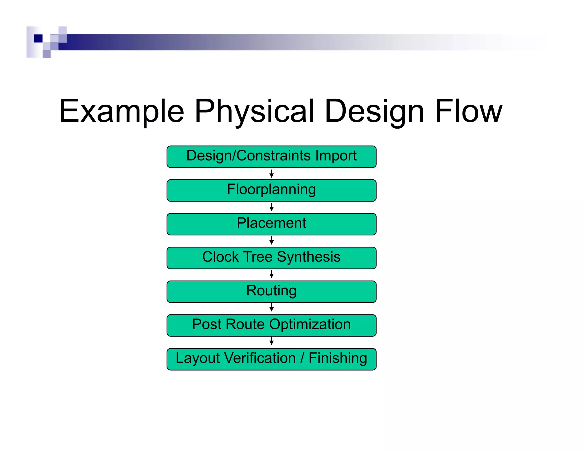
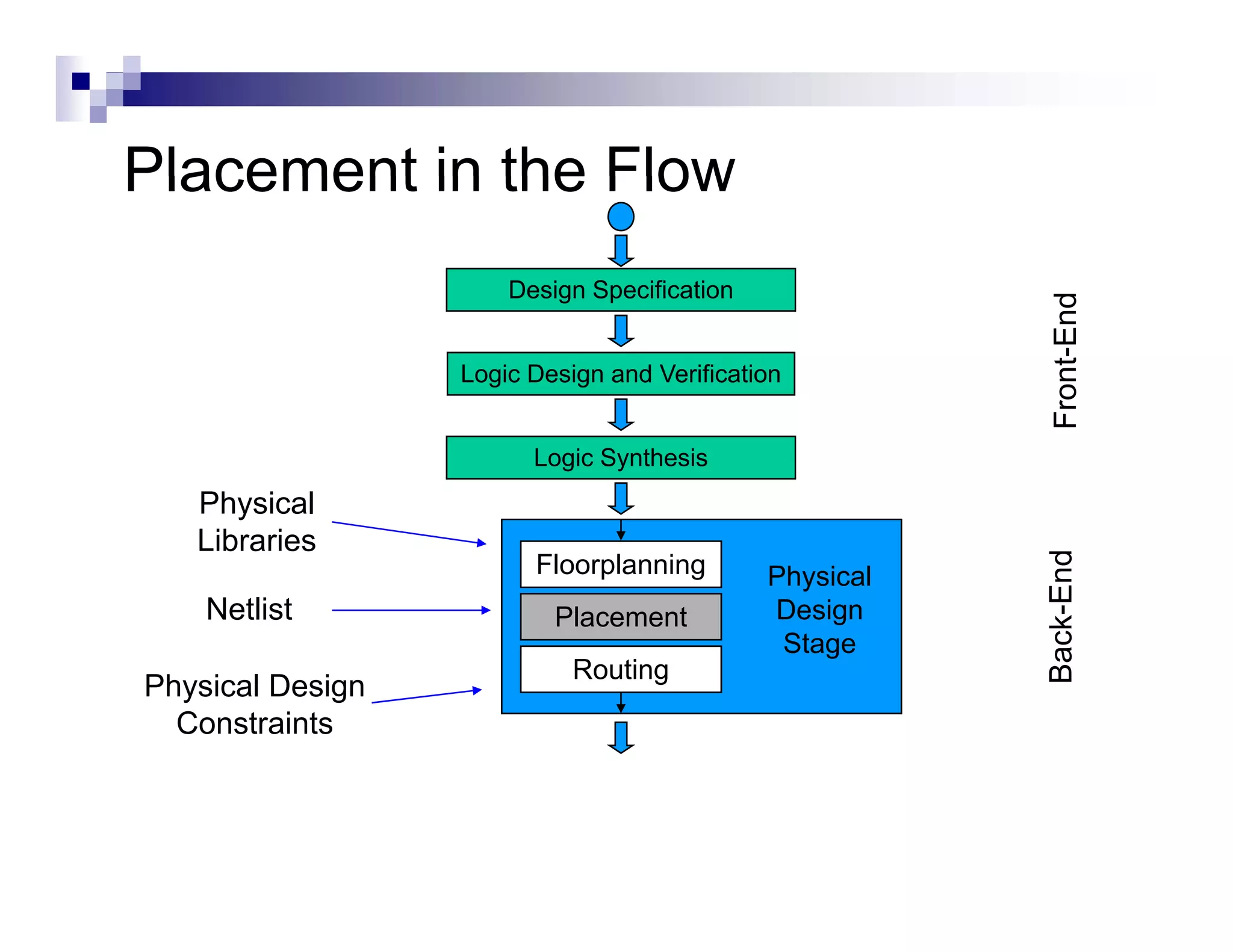
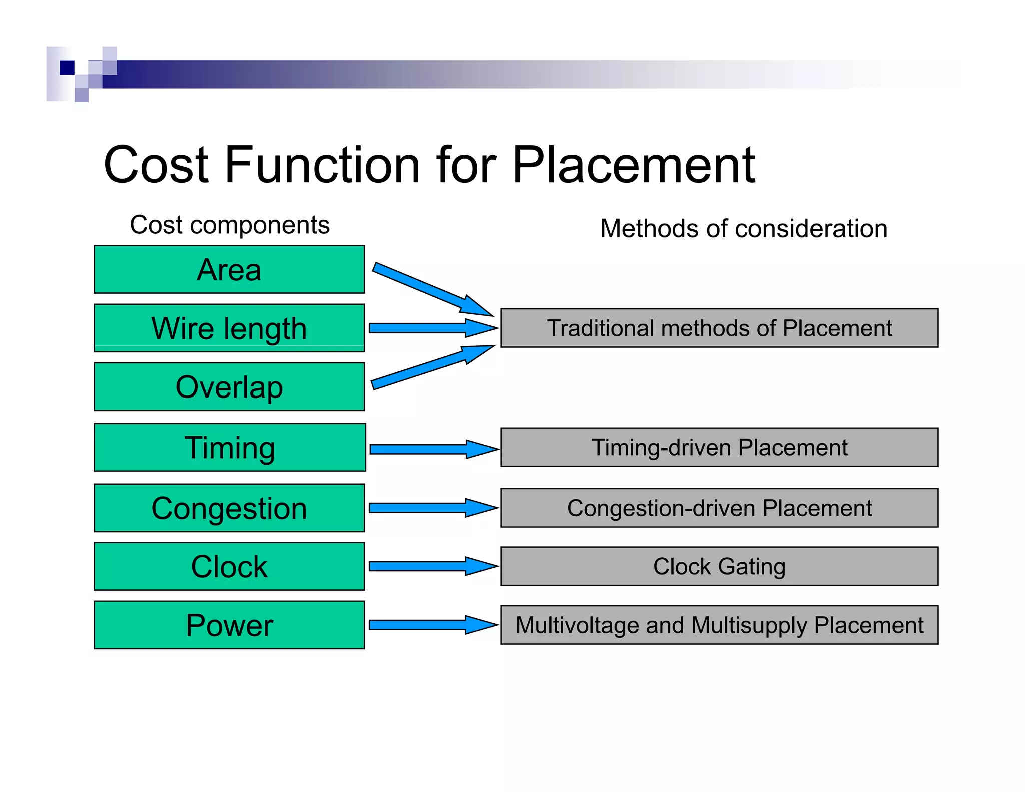
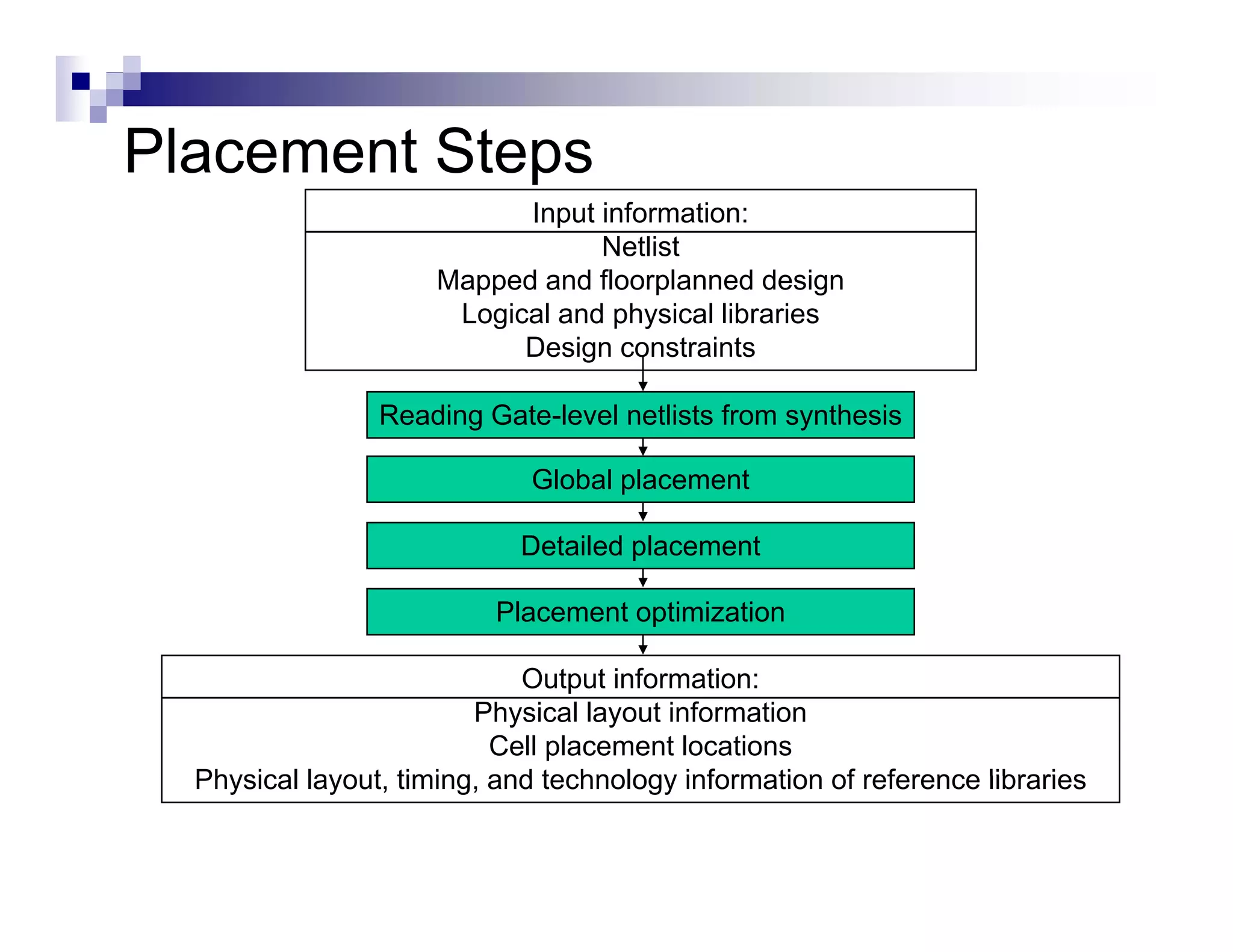
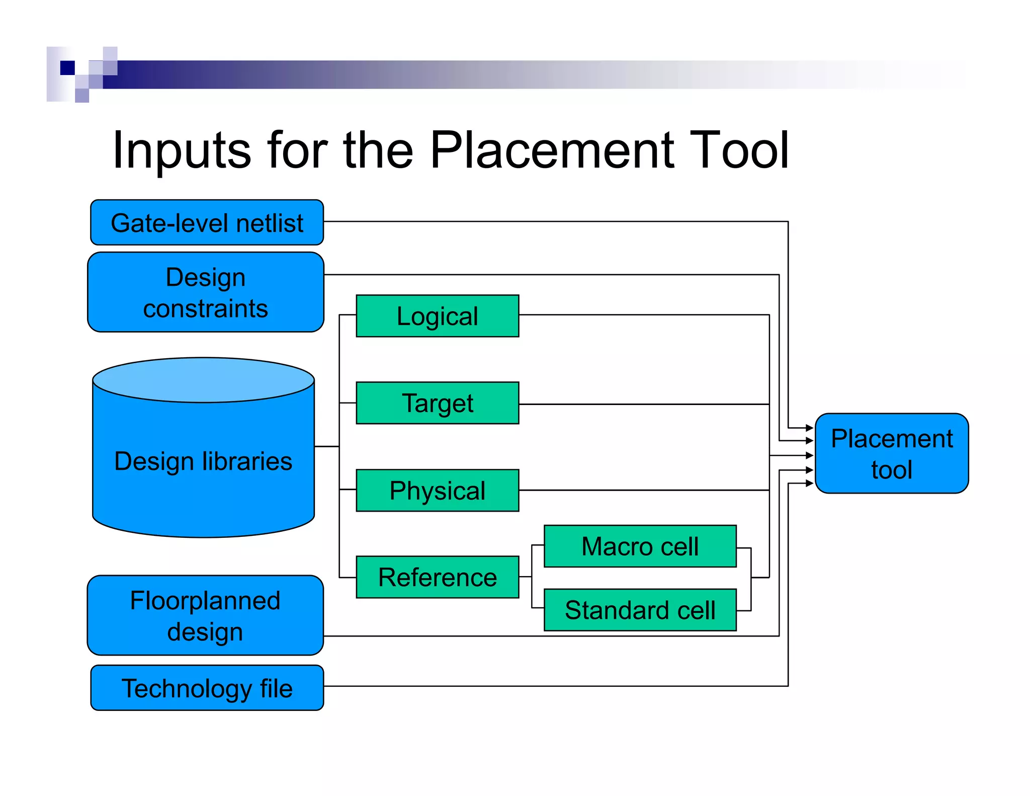
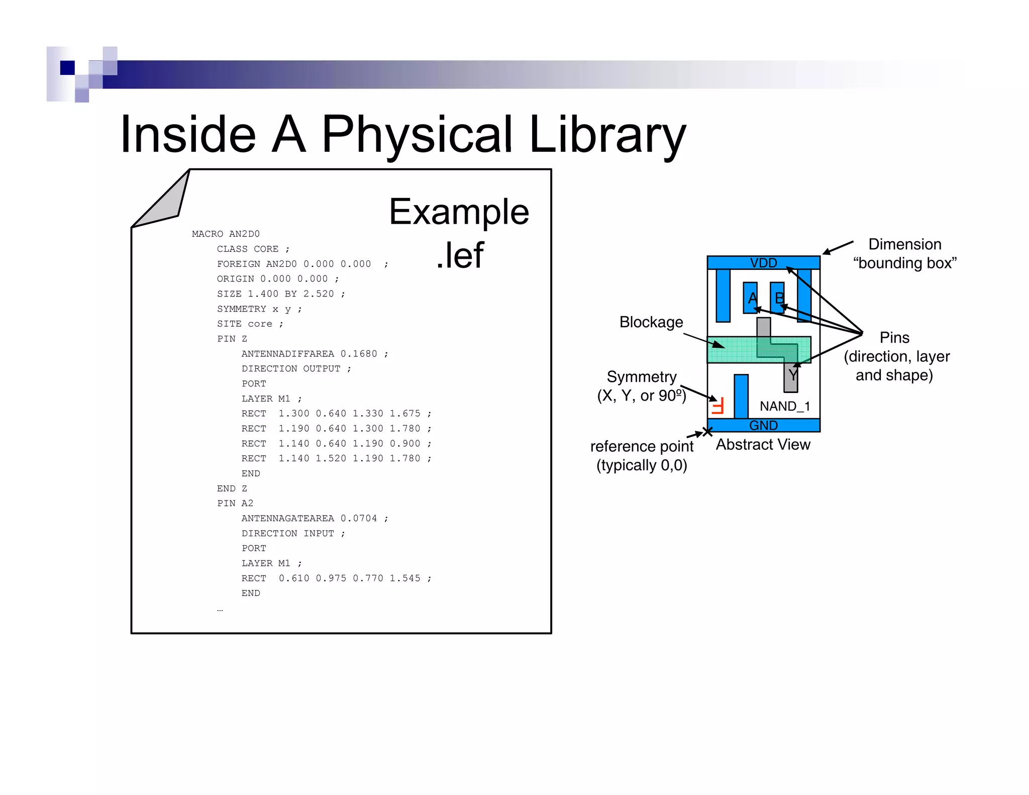
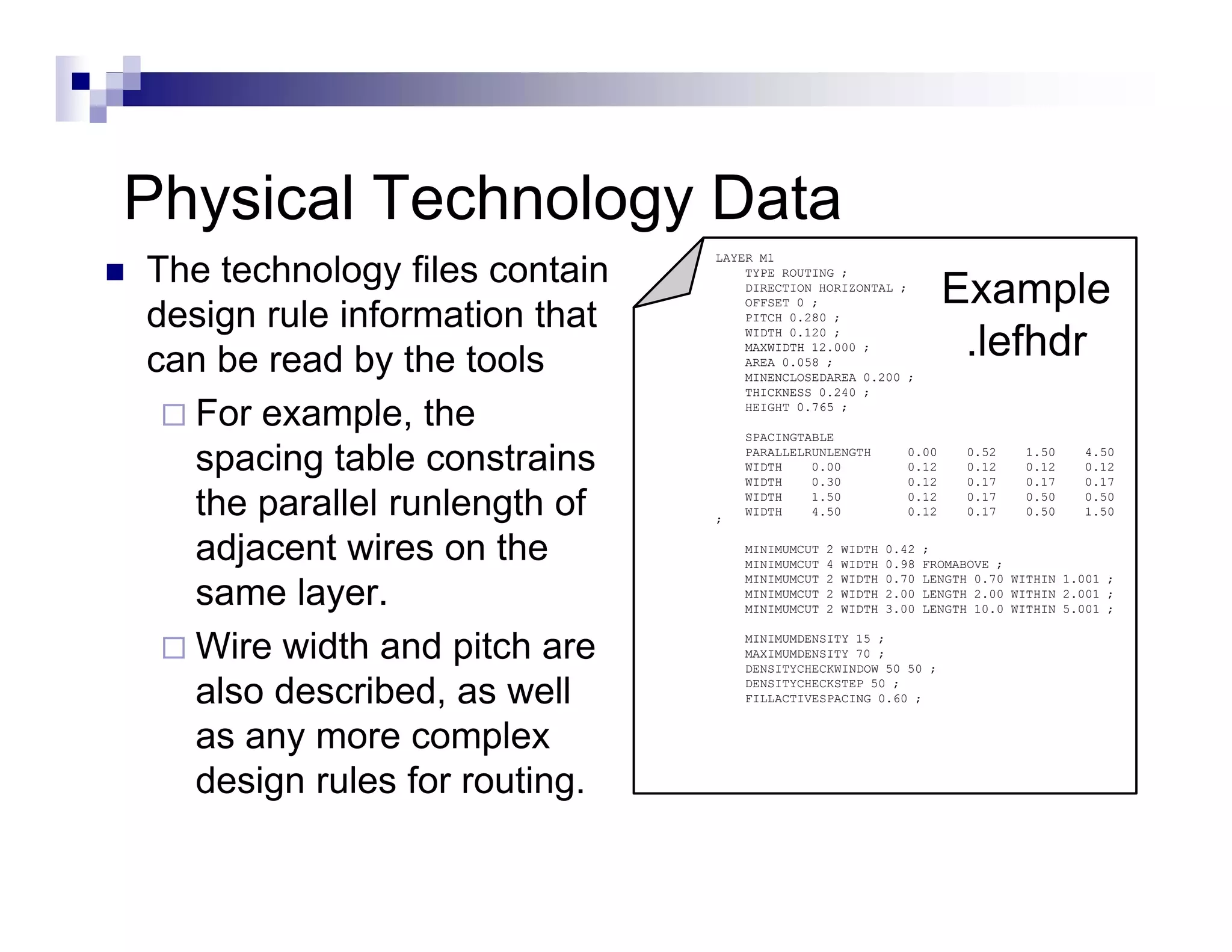
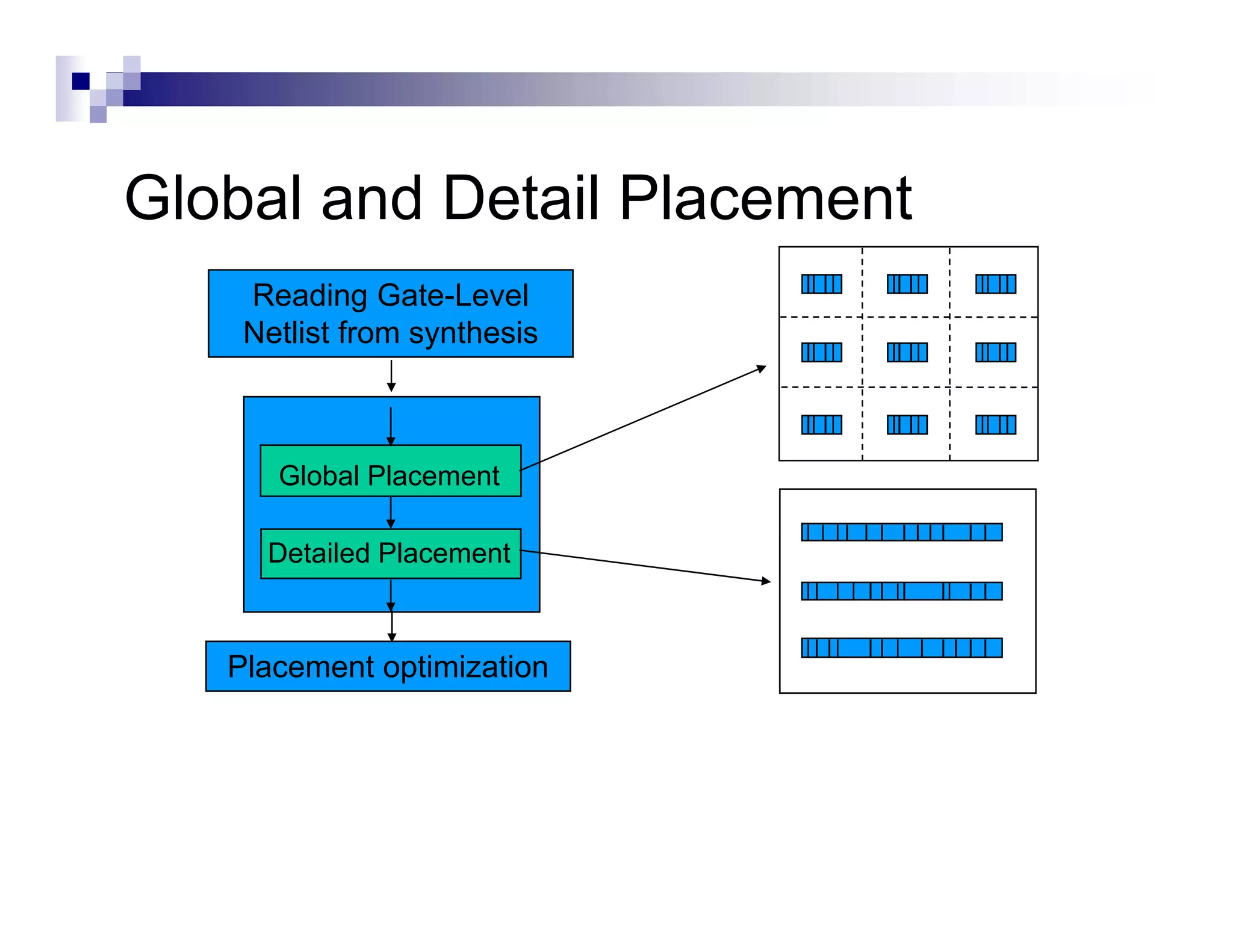
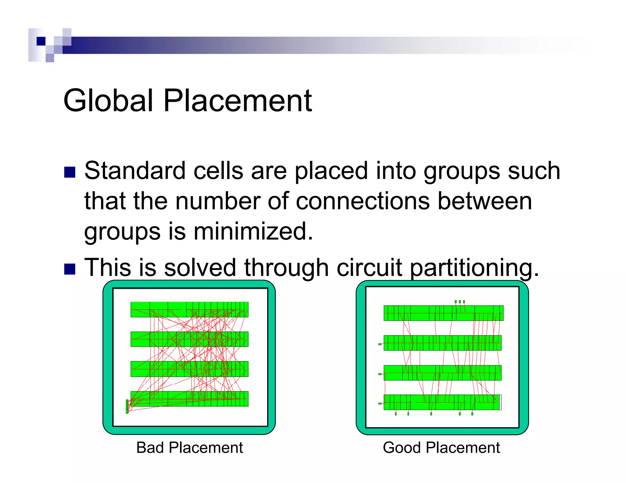
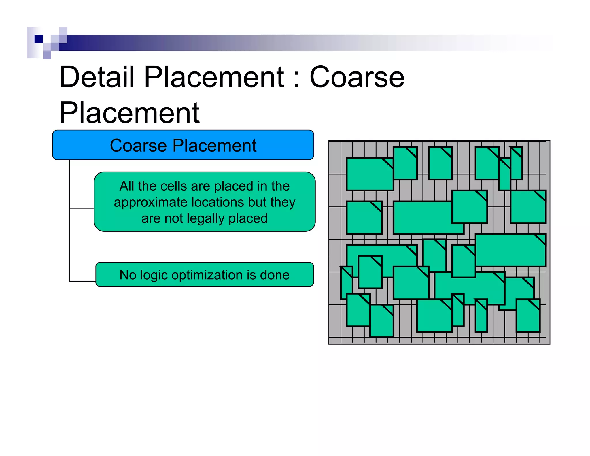
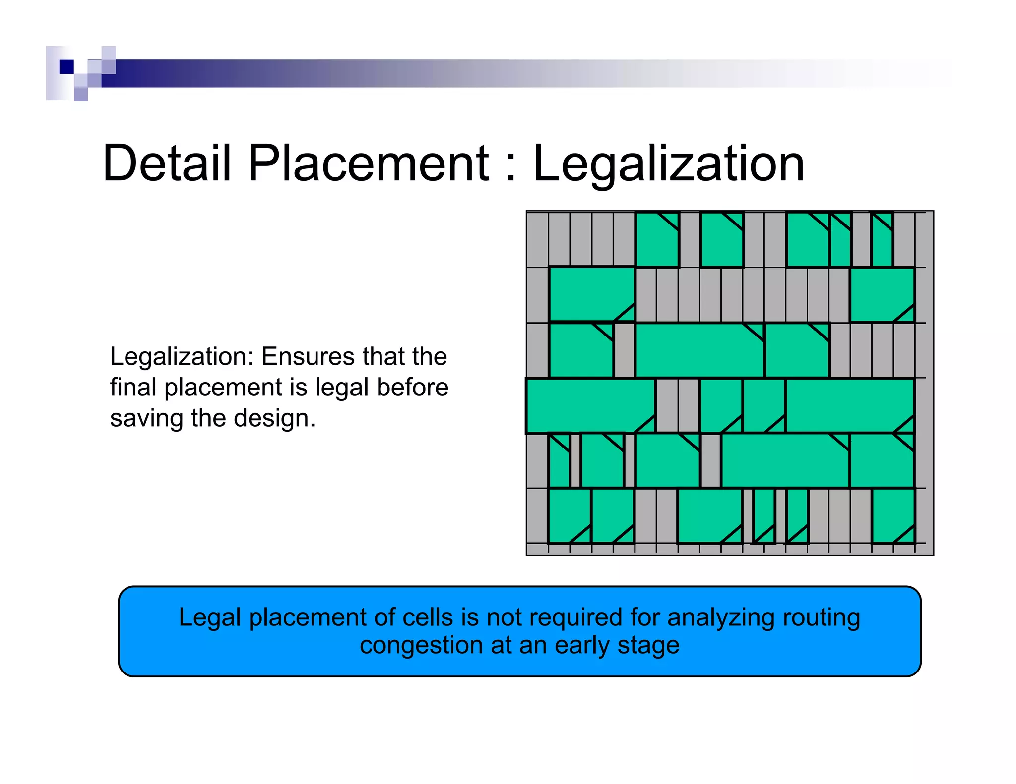
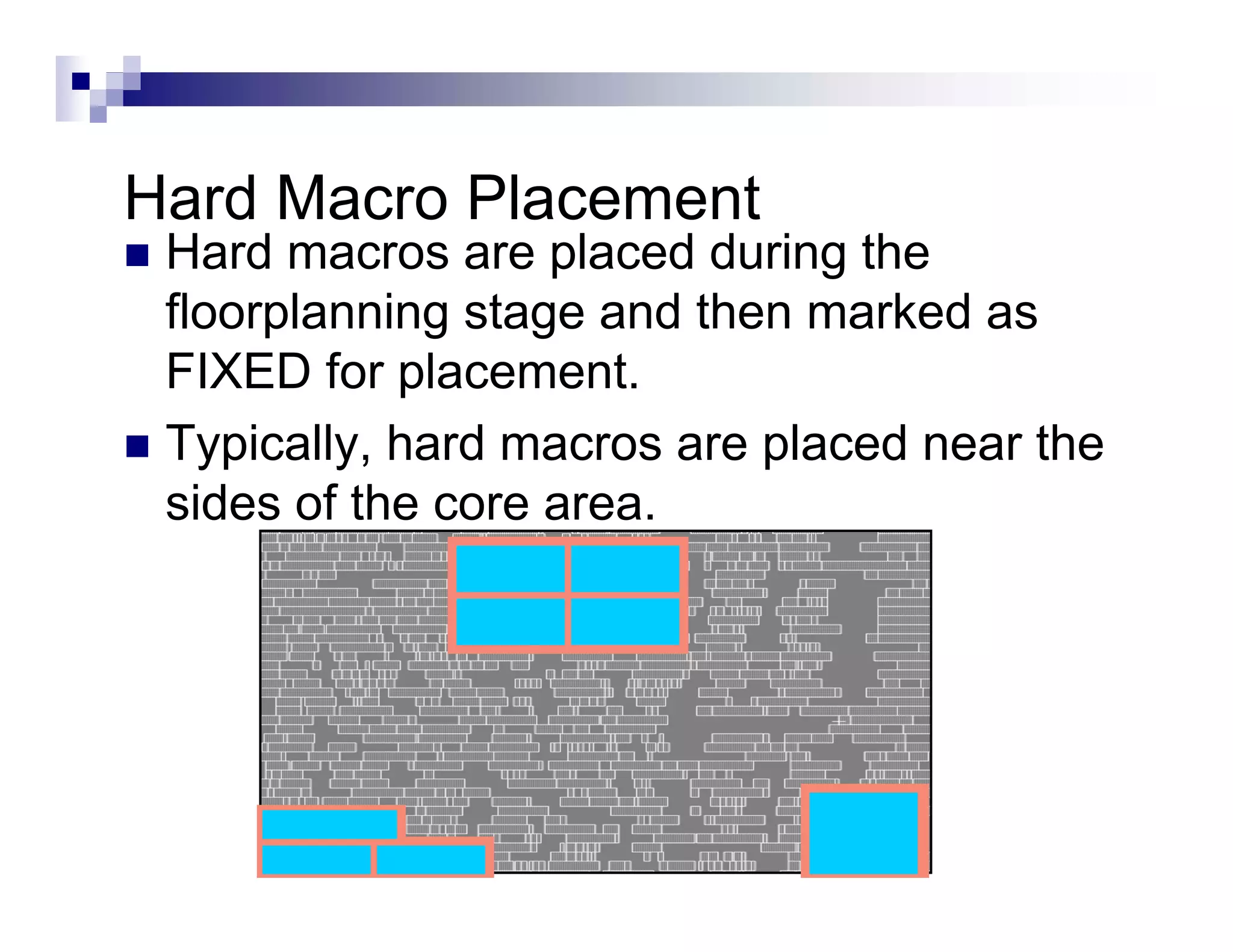
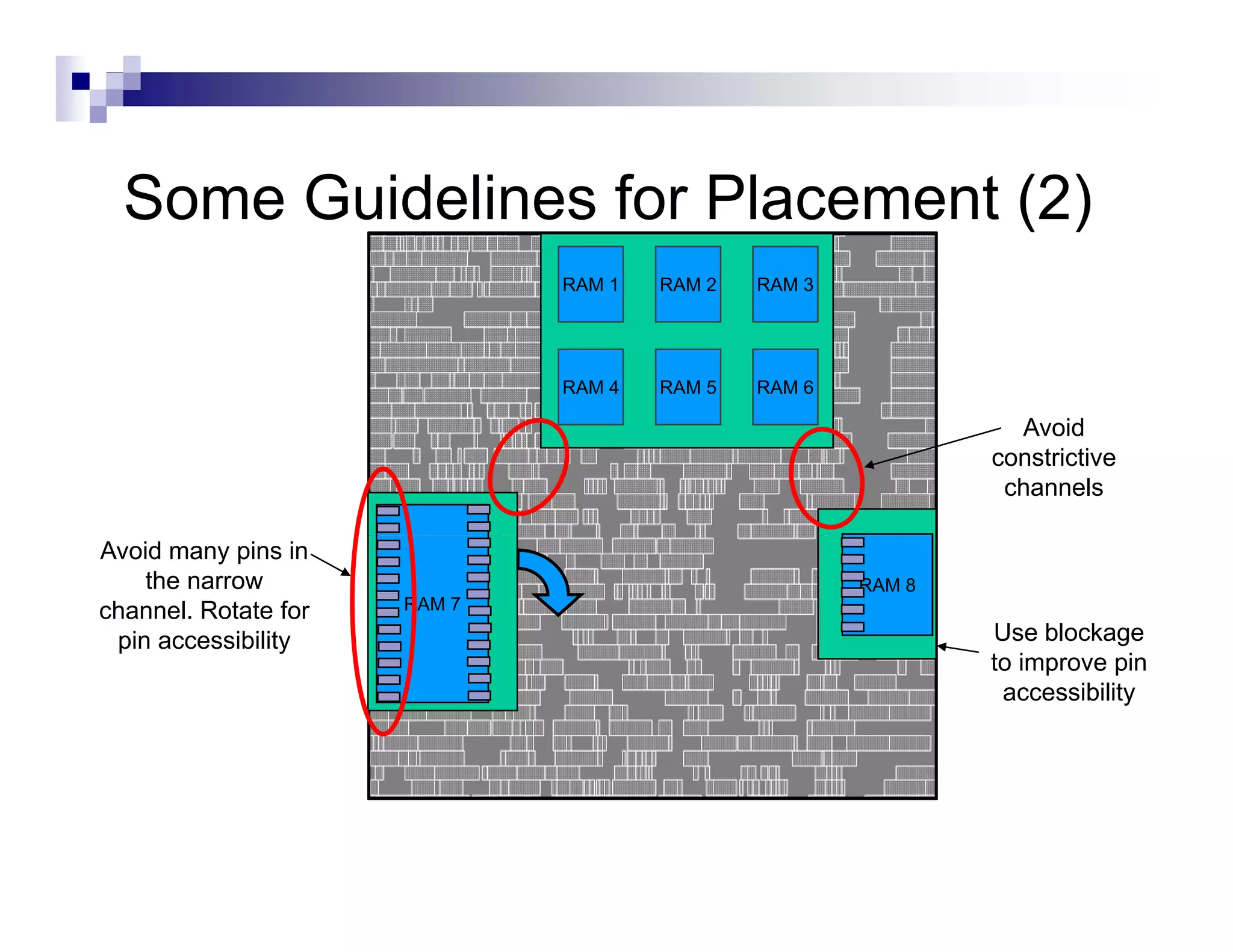
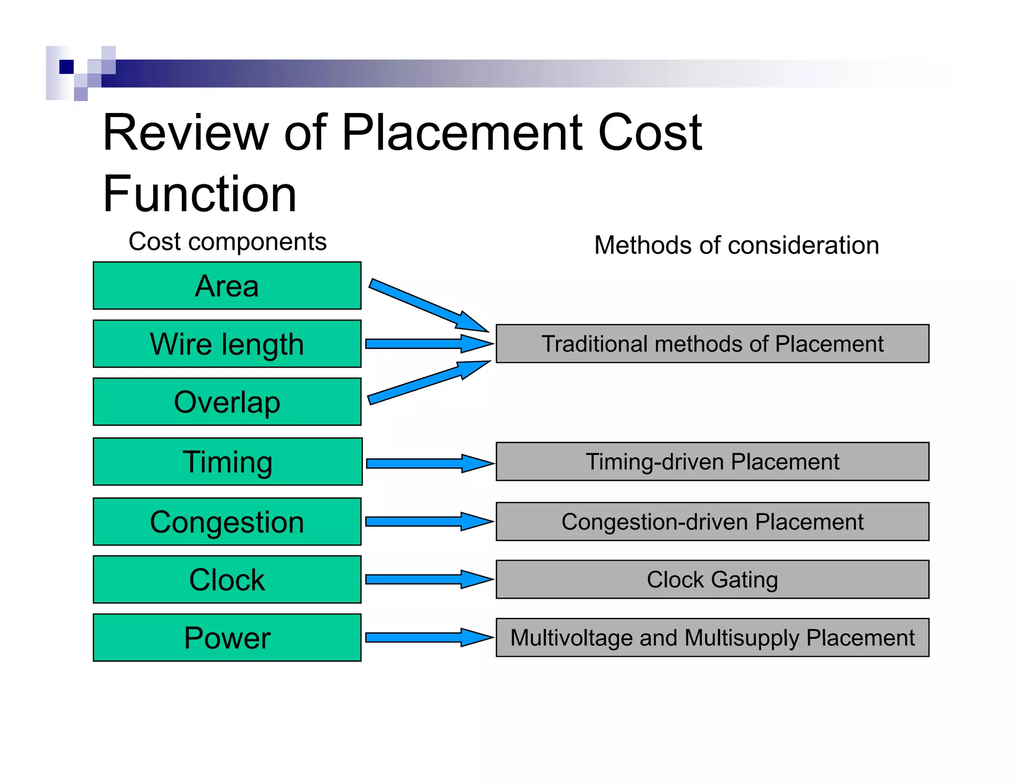
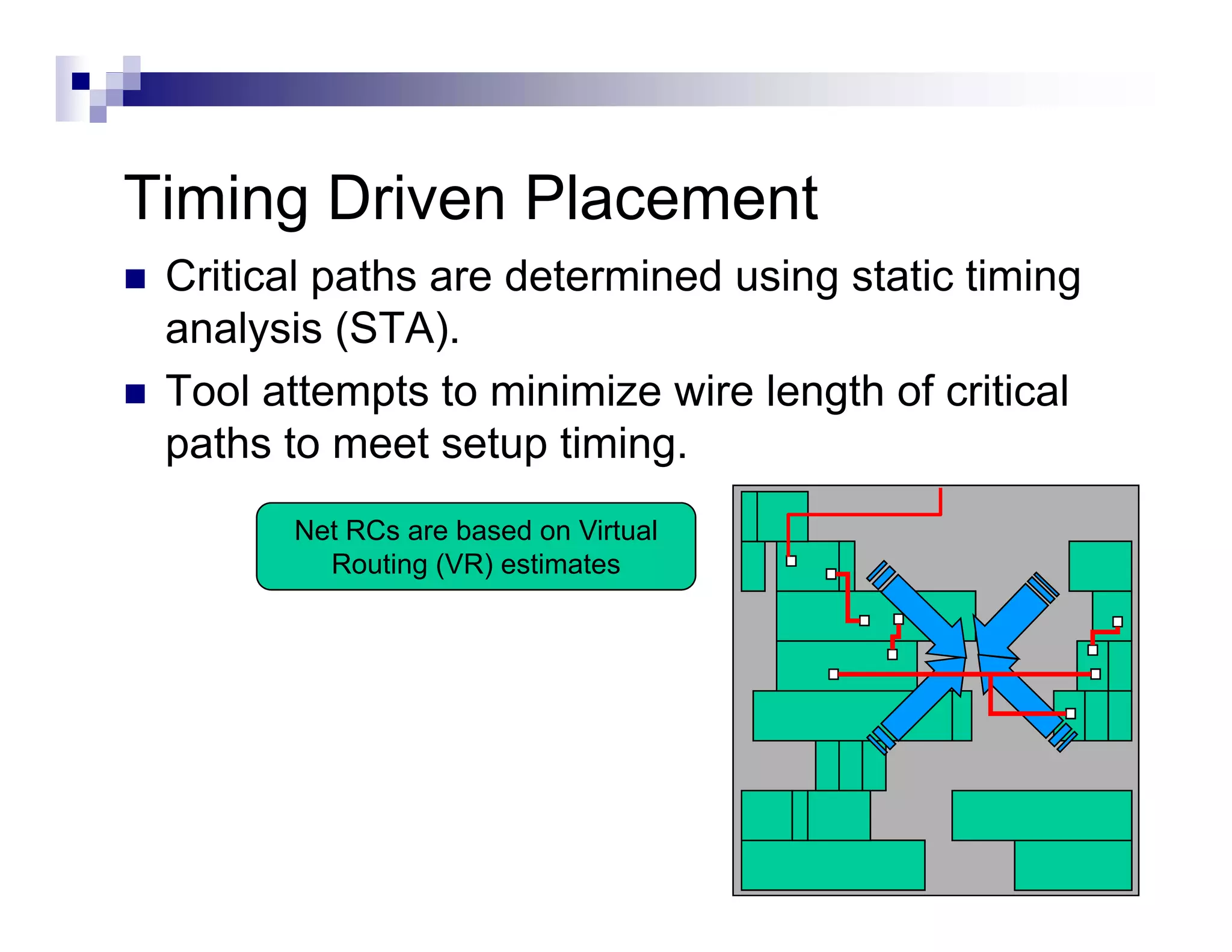
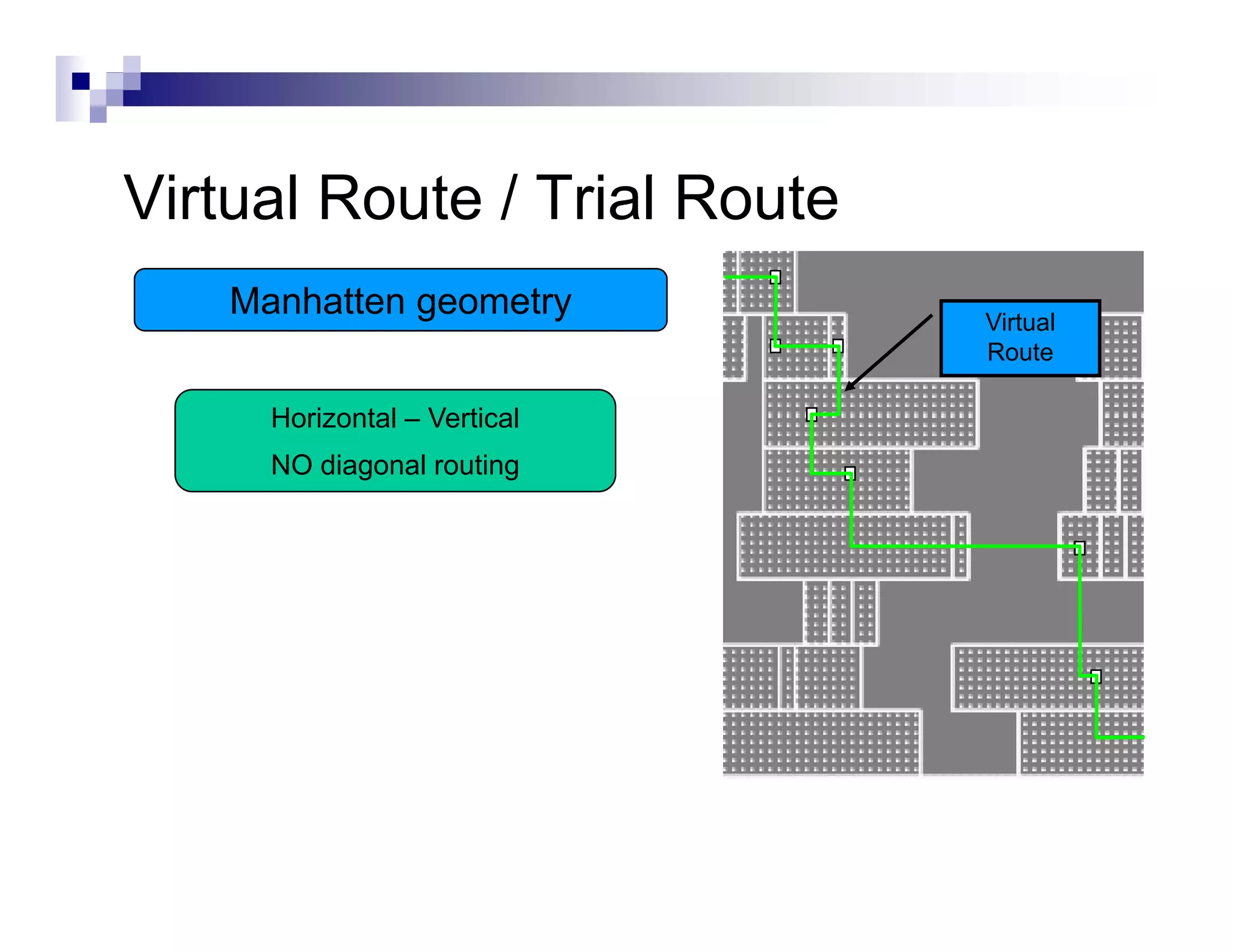
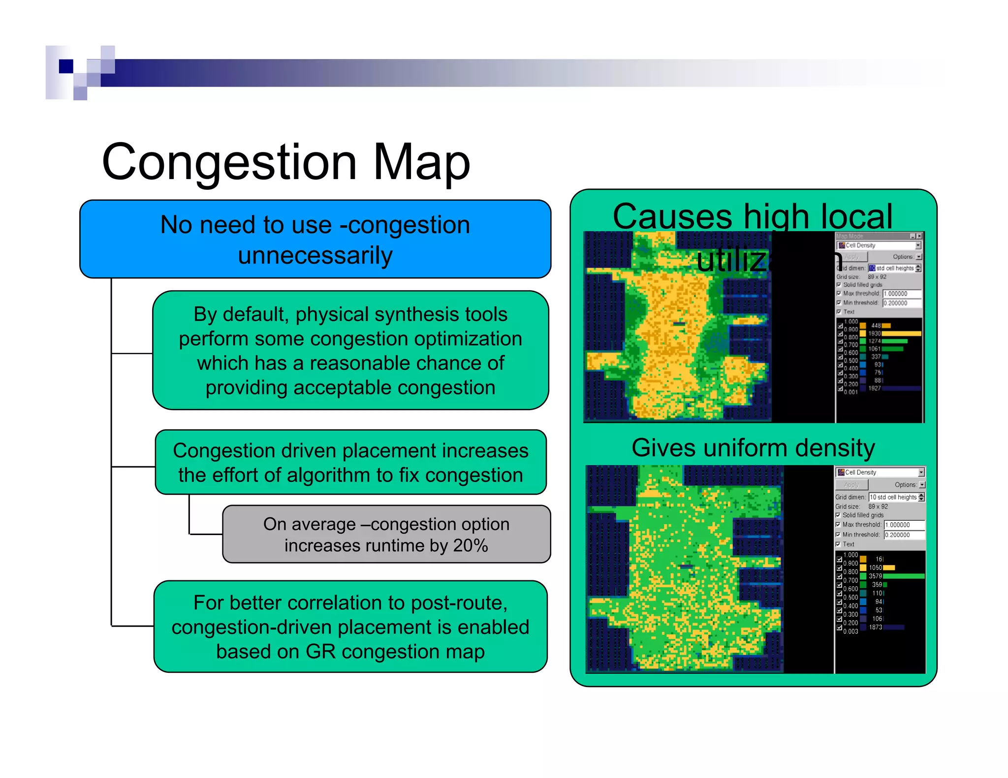
The physical design flow begins with placement which involves assigning exact locations to modules like gates and standard cells to minimize area and interconnect cost while meeting timing constraints, with the goal of enabling easier routing; placement tools take as input the netlist, floorplan, libraries, and constraints to perform global and detailed placement as well as optimization. The quality of placement significantly impacts the ability to route the design successfully.


