The document presents a comprehensive overview of Static Random Access Memory (SRAM), detailing its design, fabrication, operational characteristics, and applications. SRAM is primarily used in microprocessors due to its speed and lower power consumption compared to DRAM, although it is more expensive and less dense. The future of SRAM includes developments in non-volatile SRAM, which offers faster write times and eliminates the need for backup batteries, positioning it for various applications including RAID controllers and network routers.


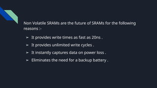
![INTRODUCTION
❖ SRAM - Static random access memory
❖ It is type of semiconductor random-access memory
❖ Uses a bistable latch circuit to store the logic
❖ Power consumption varies with frequency of operation
❖ SRAM can be used for high speed memory purpose in
microprocessors
Fig.1 A Static-RAM chip [1]](https://image.slidesharecdn.com/sram-designandfabrication-250203101652-24f0161c/85/Static-RAM-Design-and-Its-Fabrication-pptx-4-320.jpg)

![SRAM
❖ Hold data without external refresh
Fig.2 SRAM Memory Chip
[2]
❖ Simplicity : don’t require external refresh
circuitry
❖ Speed: SRAM is faster than DRAM
❖ Cost: several times more expensive than
DRAM
❖ Size: take up much more space than
DRAM
❖ Power: Consume less power than DRAM](https://image.slidesharecdn.com/sram-designandfabrication-250203101652-24f0161c/85/Static-RAM-Design-and-Its-Fabrication-pptx-8-320.jpg)
![Continued...
➢ A typical SRAM memory made up of six
MOSFETs. Each bit in SRAM is stored on 4
transistors(M1,M2,M3,M4) that forms two
cross- coupled inverter.
➢ This storage cell has two stable states which
are used to denote 0 and 1
➢ Two additional access transistors serve to
control the access to a storage cell during
read and write operation
Fig.3 6-Transistor SRAM Cell [3]](https://image.slidesharecdn.com/sram-designandfabrication-250203101652-24f0161c/85/Static-RAM-Design-and-Its-Fabrication-pptx-9-320.jpg)
![SRAM Read and Write Operation
● For write operation
● Data =1
● Datab=0
● Select=1
● For Read Operation
● Data=1
● Datab=1(Forcefully)
● Select=1
Fig. 4 Write Operation [4]
Fig. 5 Read Operation [4]](https://image.slidesharecdn.com/sram-designandfabrication-250203101652-24f0161c/85/Static-RAM-Design-and-Its-Fabrication-pptx-10-320.jpg)

![● 32,42 - Pull up
transistors
● 34,44 - Pull down
transistors
● 50,52 - NMOS
● 58 - Word line
● 54 - Bit line
● 56 - Complimentary
bit line
❏ Fig. 6 Shows the schematic diagram of one bit 6-T SRAM structure
❏ This structure is repeated over and over to form matrix of complex SRAM
IC’s
Fig. 6 [5]](https://image.slidesharecdn.com/sram-designandfabrication-250203101652-24f0161c/85/Static-RAM-Design-and-Its-Fabrication-pptx-12-320.jpg)
![● 60,62,66,68 -
Masks used for
different
purpose, placed
over one
another
● 64 - One bit of
SRAM array
❏ Fig 7 and 8 shows the relative positions of mask to be placed over one
another
❏ Perfect positioning of masks is crucial to make better quality SRAM IC’s
Fig. 8 [5]
Fig. 7 [5]](https://image.slidesharecdn.com/sram-designandfabrication-250203101652-24f0161c/85/Static-RAM-Design-and-Its-Fabrication-pptx-13-320.jpg)
![● 102 - Substrate
● 104 - Isolation
Region
● 106 - High-K gate
insulator (Hafnium
oxide)
● 108 - Another
Insulator (Titanium
Nitride)
● 110 - Dummy gate
electrode material
(Polycrystalline
silicon)
❏ Fig. 9 shows the relative positioning of one bit SRAM cell w.r.t. all masks
❏ Fig. 10 shows the cross sectional view taken along line X-X in Fig.7
❏ Basic steps of device fabrication such as oxidation, diffusion, ion implantation,
photolitiogyaphy etc are followed
Fig. 9 [5]
Fig. 10 [5]](https://image.slidesharecdn.com/sram-designandfabrication-250203101652-24f0161c/85/Static-RAM-Design-and-Its-Fabrication-pptx-14-320.jpg)
![● 116 -
Insulator
(Silicone
nitride)
● 118 -
Insulator
(SiO2)
● 120 - Hard
mask
material
❏ Two different type of insulating materials are deposited (Fig. 11)
❏ Hard mask material is deposited over dummy electrodes for selective etching
(Fig. 12)
Fig. 11 [5] Fig. 12 [5]](https://image.slidesharecdn.com/sram-designandfabrication-250203101652-24f0161c/85/Static-RAM-Design-and-Its-Fabrication-pptx-15-320.jpg)
![● 122 - Intergate
mask
● 124 - Spacer-cut
mask
❏ Intergate and Spacer-cut masks are used for patterning ‘Hard mask layer’, which
then can be used for selective etching
❏ Fig.14 shows the relative positioning of intergate and spacer-cut mask w.r.t original
arrangement
Fig. 14 [5]
Fig. 13 [5]](https://image.slidesharecdn.com/sram-designandfabrication-250203101652-24f0161c/85/Static-RAM-Design-and-Its-Fabrication-pptx-16-320.jpg)
![● 130 - Metal
Silicide
● 132 - Fill
material
(Poly-
crystalline
Si)
❏ After selective etching sharp-cornered structure is obtained (Fig.15)
❏ Implementation of metal silicide and polycrystalline Si
❏ After planarizing Fig.16 is obtained
Fig. 16 [5]
Fig. 15 [5]](https://image.slidesharecdn.com/sram-designandfabrication-250203101652-24f0161c/85/Static-RAM-Design-and-Its-Fabrication-pptx-17-320.jpg)
![● 136 - Hard
mask layer
● 142 - Gate
electrode
material
● 150,152 -
Real Gate
electrodes
● 154 -
Source
drain
contacts
❏ Hard mask layer is patterned (Fig.17), which then used for selective etching
❏ Using this Hard mask layer various connections are established, e.g. -
common gate connection between pull-up and pull-down transistors
❏ After planarizing Fig.18 is obtained
Fig. 18 [5]
Fig. 17 [5]](https://image.slidesharecdn.com/sram-designandfabrication-250203101652-24f0161c/85/Static-RAM-Design-and-Its-Fabrication-pptx-18-320.jpg)


![➢ The first solid state memory chip
➢ It is a 64-bit SRAM
➢ It applied the newly developed Schottky Bipolar technology
April 1969.
Fig. 19 Intel 3101 [6].](https://image.slidesharecdn.com/sram-designandfabrication-250203101652-24f0161c/85/Static-RAM-Design-and-Its-Fabrication-pptx-21-320.jpg)
![➢ The first MOS memory chip
➢ A 256-bit SRAM
➢ Produced in with Silicon gate MOS technology
➢ It gave intel the edge it needed to produce high density memories
July 1969
Fig. 20 Intel 1101
[7]](https://image.slidesharecdn.com/sram-designandfabrication-250203101652-24f0161c/85/Static-RAM-Design-and-Its-Fabrication-pptx-22-320.jpg)
![Fig. 21 Intel Core 2 Duo E6300
Processor [8]
Fig. 22 Latest Intel Core i9-9900T
Processor ( 16M Cache, Up to 4.40 GHz )
[9]
➢ Modern SRAM’s are generally integrated inside microprocessors](https://image.slidesharecdn.com/sram-designandfabrication-250203101652-24f0161c/85/Static-RAM-Design-and-Its-Fabrication-pptx-23-320.jpg)
![Fig. 23 SRAM
Scaling Trend [10]
➢ SRAM trends shows cell area reduced by half every two years](https://image.slidesharecdn.com/sram-designandfabrication-250203101652-24f0161c/85/Static-RAM-Design-and-Its-Fabrication-pptx-24-320.jpg)

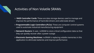
![Fig. 24 RAID Controller Card
[11]
Fig. 25 Programmable Logic
Controller [12]
Fig. 26 Network
Router [13]
Fig. 28 Electronic Gaming
Machine [14]](https://image.slidesharecdn.com/sram-designandfabrication-250203101652-24f0161c/85/Static-RAM-Design-and-Its-Fabrication-pptx-28-320.jpg)
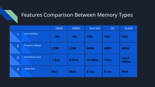
![Random Transaction Rate (RTR) - Random Transaction Rate
(RTR) is the number of fully random read or write transactions
a memory can perform every second.
➢ Cypress's QDR-IV SRAM provides RTR up to 2132 MT/s
➢ This level of performance is critical to enable the next
generation of high performance systems
Fig. 29 RTR [15]. Fig. 39 QDR SRAM
[15].](https://image.slidesharecdn.com/sram-designandfabrication-250203101652-24f0161c/85/Static-RAM-Design-and-Its-Fabrication-pptx-29-320.jpg)
![Sources
● [1]https://en.m.wikipedia.org/wiki/Static_random-access_memory
● [2]
https://encrypted-tbn0.gstatic.com/images?q=tbn%3AANd9GcTt6M5kR4jsgp9At1BE3orl2vgMXElW-ii
Cs-4blQYRSMQo2VP6
● [3]https://commons.wikimedia.org/wiki/File:6t-SRAM-cell.png
● [4]https://www.slideshare.net/tipusultan3150/sram-dram
● [5]http://www.freepatentsonline.com/20130193516.pdf
● [6]https://newsroom.intel.com/news/intel-at-50-intels-first-product-3101/
● [7]
https://commons.wikimedia.org/wiki/File:Intel_1101_1a.jpghttps://commons.wikimedia.org/wiki/File:Intel_1101_1a.
● [8]https://en.wikipedia.org/wiki/Conroe_(microprocessor)#Conroe
● [9]https://hexus.net/tech/news/cpu/133988-intel-core-i9-9900t-tested-multiple-times-geekbench-4/
● [10]https://fuse.wikichip.org/news/525/iedm-2017-isscc-2018-intels-10nm-switching-to-cobalt-interconnects/5/
● [11]https://www.esaitech.com/lsi-logic-ser523-6-port-raid-controllercard.html
● [12]https://images.app.goo.gl/p2bwpxSDR9uNsNuG6
● [13]https://www.lifewire.com/how-routers-work-816456
● [14]
http://www.emissourian.com/local_news/county/electronic-gaming-machines-in-use-in-franklin-county-not-regulated/](https://image.slidesharecdn.com/sram-designandfabrication-250203101652-24f0161c/85/Static-RAM-Design-and-Its-Fabrication-pptx-31-320.jpg)


![MID_TERM_PPT[1].pdf128228282828828282828282](https://cdn.slidesharecdn.com/ss_thumbnails/midtermppt1-250106164820-22402fb8-thumbnail.jpg?width=640&height=640&fit=bounds)


