Downloaded 2,088 times


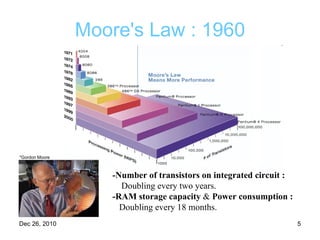
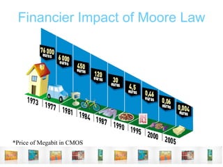
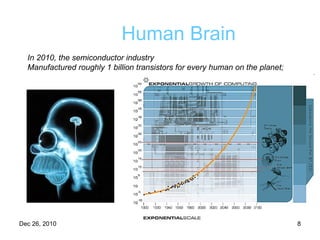


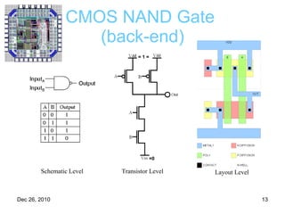
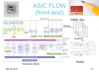
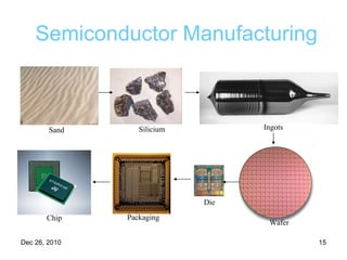


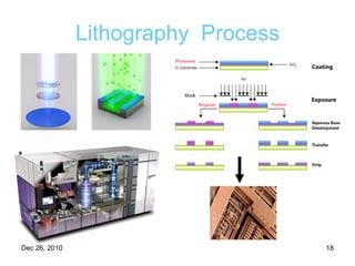


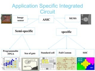
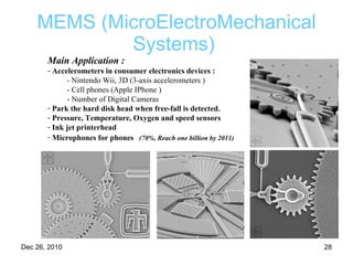
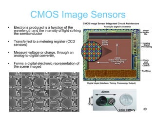
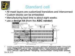
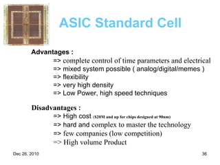
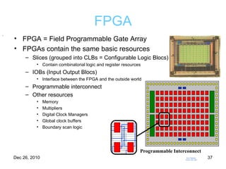
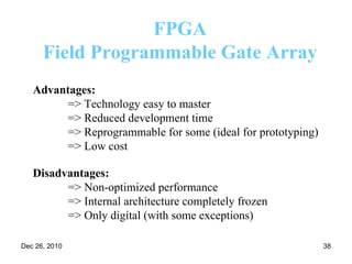
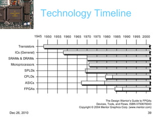
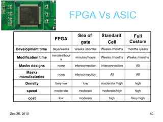
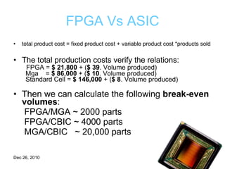
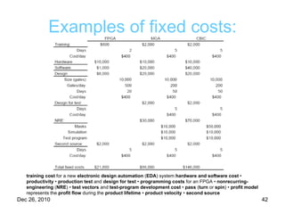
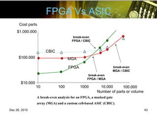
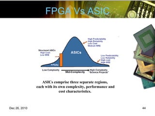
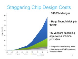

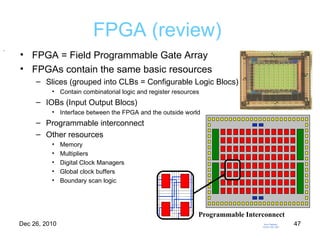


The document provides an overview of the history and evolution of semiconductors and integrated circuits from 1947 to present. It discusses key inventions and milestones such as the transistor in 1947, the integrated circuit in 1961, and Moore's Law predicting transistor doubling every two years. It also covers different chip design approaches including full custom, standard cell, gate arrays, and FPGAs, along with their relative costs, performance, and design complexities.


![Getting Started with Apache Spark: Big Data Made Simple [Free Meetup]](https://cdn.slidesharecdn.com/ss_thumbnails/apachesparkgettingstarted-260203175547-8361bcc3-thumbnail.jpg?width=640&height=640&fit=bounds)


