Introduction
Storage of largeinformation.
Low Power Memory requirement.
Advanced fabrication technologies and compact design.
On chip memories in VLSI.
4.
4
Classification of SemiconductorMemory
Based on R/W
Operation
RAM (Volatile)
ROM (Non-
volatile)
Based on Fabrication
Memory using Bipolar transistor
Memory using unipolar transistor
(MOS)
5.
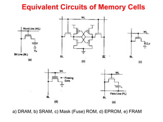
Equivalent Circuits ofMemory Cells
a) DRAM, b) SRAM, c) Mask (Fuse) ROM, d) EPROM, e) FRAM
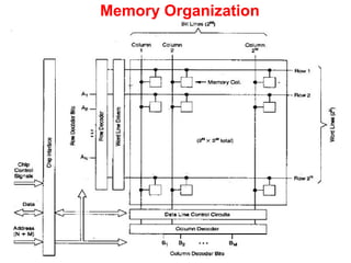
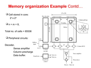
Memory organization ExampleContd…
Cell stored in core:
2n
x 2m
n = m = 8,
Total no. of cells = 65536
Peripheral circuits:
Decoder,
Sense amplifier
Column precharge
Data buffer.
8.
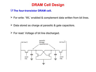
DRAM Cell Design
The four-transistor DRAM cell.
For write: ‘WL’ enabled & complement data written from bit lines.
Data stored as charge at parasitic & gate capacitors.
For read: Voltage of bit line discharged.
9.
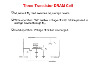
Three-Transistor DRAM Cell
M1 write & M2 read switches, M3 storage device.
Write operation: ‘WL’ enable, voltage of write bit line passed to
storage device through M1.
Read operation: Voltage of bit line discharged.
M1
M2
M3
10.
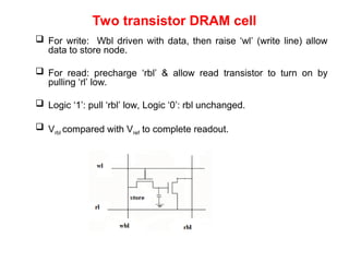
Two transistor DRAMcell
For write: Wbl driven with data, then raise ‘wl’ (write line) allow
data to store node.
For read: precharge ‘rbl’ & allow read transistor to turn on by
pulling ‘rl’ low.
Logic ‘1’: pull ‘rbl’ low, Logic ‘0’: rbl unchanged.
Vrbl compared with Vref to complete readout.
11.
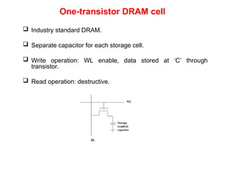
One-transistor DRAM cell
Industry standard DRAM.
Separate capacitor for each storage cell.
Write operation: WL enable, data stored at ‘C’ through
transistor.
Read operation: destructive.
12.
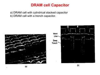
DRAM cell Capacitor
a)DRAM cell with cylindrical stacked capacitor
b) DRAM cell with a trench capacitor.
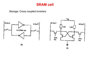
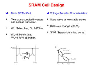
SRAM Cell Design
Basic SRAM Cell
Two cross coupled invertors
and access transistor.
WL: Select line, BL R/W line.
WL=0: Hold state,
WL=1 R/W operation.
Voltage Transfer Characteristics
Store valve at two stable states
Cell state change with Vth.
SNM: Separation in two curve.
16.
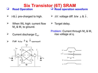
Six Transistor (6T)SRAM
Read Operation
& pre-charged to high.
When WL high: current flow
M3 & M1 to ground.
Current discharge Cbit.
Diff. b/w & sensed.
Read operation waveform
∆V: voltage diff. b/w & .
Target delay.
Problem: Current through M3 & M1
rise voltage at q.
b
b
b b
b
b
17.
Six Transistor (6T)SRAM Contd…
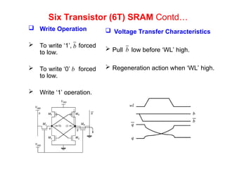
Write Operation
To write ‘1’, forced
to low.
To write ‘0’ forced
to low.
Write ‘1’ operation.
Voltage Transfer Characteristics
Pull low before ‘WL’ high.
Regeneration action when ‘WL’ high.
b
b
b
18.
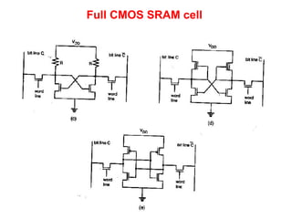
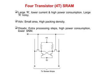
Four Transistor (4T)SRAM
Large ‘R’, lower current & high power consumption. Large
‘R’ noisy.
Adv: Small area, High packing density.
Disadv: Extra processing steps, high power consumption,
lower SNM.
19.
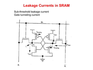
Leakage Currents inSRAM
Sub-threshold leakage current
Gate tunneling current
20.
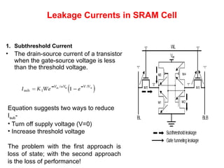
Leakage Currents inSRAM Cell
1. Subthreshold Current
• The drain-source current of a transistor
when the gate-source voltage is less
than the threshold voltage.
Equation suggests two ways to reduce
Isub-
• Turn off supply voltage (V=0)
• Increase threshold voltage
The problem with the first approach is
loss of state; with the second approach
is the loss of performance!
21.
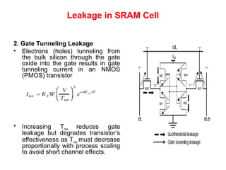
Leakage in SRAMCell
2. Gate Tunneling Leakage
• Electrons (holes) tunneling from
the bulk silicon through the gate
oxide into the gate results in gate
tunneling current in an NMOS
(PMOS) transistor
• Increasing Tox reduces gate
leakage but degrades transistor’s
effectiveness as Tox must decrease
proportionally with process scaling
to avoid short channel effects.
22.
Static Noise Margin(SNM)
• SNM quantifies the amount of voltage noise required at the internal
nodes of a bitcell to flip the cell’s content.
• Degraded SNM limits voltage scaling for SRAM designs.
23.
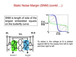
Static Noise Margin(SNM) (contd …)
Inverter
Inverter 1
WL
BLB
BL
Q QB
M1
M2
M3
M4
M5
M6
VN
VN
To obtain it, the voltage at Q is plotted
against QB for the sweep from left to right
and then right to left
SNM is length of side of the
largest embedded square
on the butterfly curve
24.
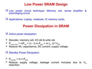
Low Power SRAMDesign
Low power circuit technique: Memory cell, sense amplifier &
precharging circuit.
Applications: Laptop, notebook, IC memory cards.
Power Dissipation in SRAM
Active power dissipation:
Decoder, memory cell, I/O ckt & write ckt.
Pmem-array = mPact + (n - l) m Pleak + m Idc ∆t f VDD.
Reduce WL capacitance, DC current, supply voltage.
Standby Power Dissipation
Pstandby = m n Pleak
Reduce supply voltage, leakage current increase due to Vth
reduction.
25.
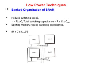
Low Power Techniques
Banked Organization of SRAM
Reduce switching speed.
n = R x C, Total switching capacitance = R x C x Ccell
Splitting memory reduce switching capacitance.
(R x C x Ccell)/B
26.
Low Power TechniquesContd…
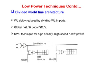
Divided world line architecture
WL delay reduced by dividing WL in parts.
Global ‘WL’ & Local ‘WL’s.
DWL technique for high density, high speed & low power.
27.
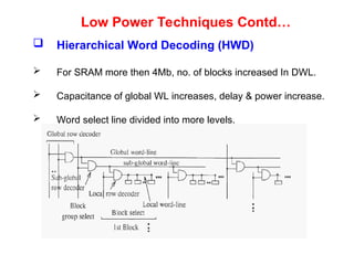
Low Power TechniquesContd…
Hierarchical Word Decoding (HWD)
For SRAM more then 4Mb, no. of blocks increased In DWL.
Capacitance of global WL increases, delay & power increase.
Word select line divided into more levels.
28.
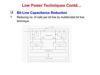
Low Power TechniquesContd…
Bit-Line Capacitance Reduction
Reducing no. of cells per bit line by multidivided bit line
technique.
29.
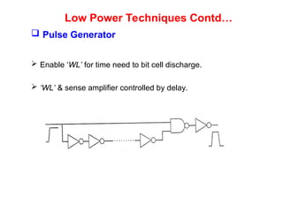
Low Power TechniquesContd…
Pulse Generator
Enable ‘WL’ for time need to bit cell discharge.
‘WL’ & sense amplifier controlled by delay.
30.
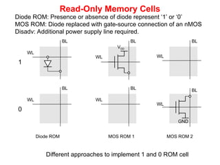
Read-Only Memory Cells
WL
BL
WL
BL
1
WL
BL
WL
BL
WL
BL
0
VDD
WL
BL
GND
DiodeROM MOS ROM 1 MOS ROM 2
Diode ROM: Presence or absence of diode represent ‘1’ or ‘0’
MOS ROM: Diode replaced with gate-source connection of an nMOS
Disadv: Additional power supply line required.
Different approaches to implement 1 and 0 ROM cell
31.
MOS ROM
WL [0]
VDD
BL[0]
WL [1]
WL [2]
WL [3]
Vbias
BL [1]
Pull-down loads
BL [2] BL [3]
VDD
4x4 Array: Overhead of supply lines reduced by sharing b/w cells. This
requires the mirroring of the odd cells around the horizontal axis.
32.
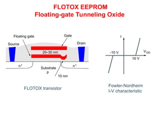
Non-Volatile Memories
The Floating-gateAvalanche-injection transistor (FAMOS)
Floating gate
Source
Substrate
Gate
Drain
n+ n+_
p
tox
tox
Device cross-section Schematic symbol
G
S
D
An extra polysilicon strip is inserted b/w gate and channel.
Double the oxide thickness, Vth increased.
High Vds create high electric field and causes avalanche injection.
Hot electron effect.
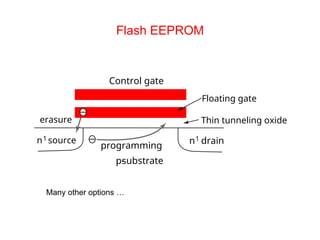
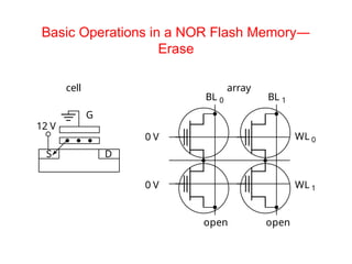
Basic Operations ina NOR Flash Memory―
Erase
S D
12 V
G
cell array
BL 0 BL 1
open open
WL 0
WL 1
0 V
0 V
39.
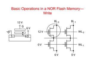
Basic Operations ina NOR Flash Memory―
Write
S D
12 V
6 V
G
BL 0 BL 1
6 V 0 V
WL 0
WL 1
12 V
0 V
40.
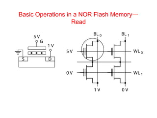
Basic Operations ina NOR Flash Memory―
Read
5 V
1 V
G
S D
BL 0 BL 1
1 V 0 V
WL 0
WL 1
5 V
0 V
41.
Memory Architecture: Decoders
Word0
Word 1
Word 2
WordN22
WordN21
Storage
cell
M bits M bits
N
words
S0
S1
S2
SN22
A0
A1
AK 21
K 5 log2N
SN21
Word 0
Word 1
Word 2
WordN22
WordN21
Storage
cell
S0
Input-Output
(M bits)
Intuitive architecture for N x M memory
Too many select signals:
N words == N select signals
K = log2N
Decoder reduces the number of select signals
Input-Output
(M bits)
Decoder
42.
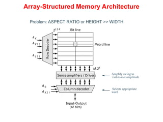
Row
Decoder
Bit line
2L 2K
Word line
A K
A K 1 1
A L 2 1
A 0
M.2K
A K 2 1
Sense amplifiers / Drivers
Column decoder
Input-Output
(M bits)
Array-Structured Memory Architecture
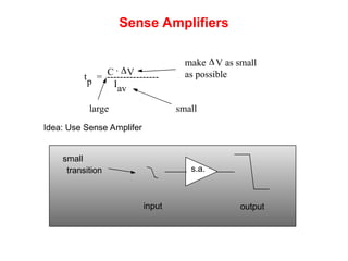
Problem: ASPECT RATIO or HEIGHT >> WIDTH
Amplify swing to
rail-to-rail amplitude
Selects appropriate
word
43.
Row Decoders
Collection of2M
complex logic gates
Organized in regular and dense fashion
(N)AND Decoder
NOR Decoder
4-input pass-transistor basedcolumn decoder
Advantages: speed (tpd does not add to overall memory access time)
Only one extra transistor in signal path
Disadvantage: Large transistor count
2-input NOR decoder
A0
S0
BL 0 BL 1 BL 2 BL 3
A1
S1
S2
S3
D
47.
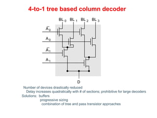
4-to-1 tree basedcolumn decoder
Number of devices drastically reduced
Delay increases quadratically with # of sections; prohibitive for large decoders
buffers
progressive sizing
combination of tree and pass transistor approaches
Solutions:
BL 0 BL 1 BL 2 BL 3
D
A0
A0
A1
A1
48.
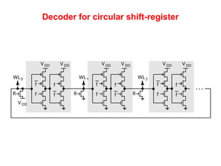
Decoder for circularshift-register
V DD
V DD
R
WL0
V DD
f
f
f
f
V DD
R
WL1
V DD
f
f
f
f
V DD
R
WL2
V DD
f
f
f
f
• • •
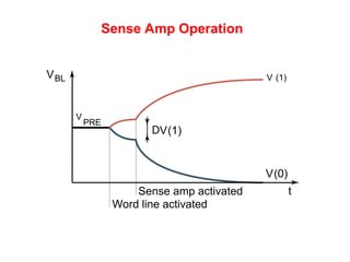
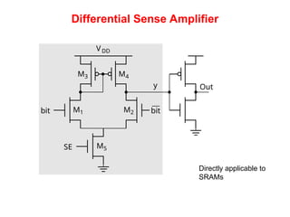
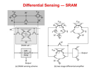
Differential Sensing ―SRAM
V DD
V DD
V DD
V DD
BL
EQ
Diff.
Sense
Amp
(a) SRAM sensing scheme (b) two stage differential amplifier
SRAM cell i
WL i
2
x
x
V DD
Output
BL
PC
M3
M1
M5
M2
M4
x
SE
SE
SE
Output
SE
x
2
x 2
x
53.
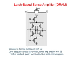
Latch-Based Sense Amplifier(DRAM)
Initialized in its meta-stable point with EQ
Once adequate voltage gap created, sense amp enabled with SE
Positive feedback quickly forces output to a stable operating point.
EQ
VDD
BL BL
SE
SE


![MOS ROM
WL [0]
VDD
BL [0]
WL [1]
WL [2]
WL [3]
Vbias
BL [1]
Pull-down loads
BL [2] BL [3]
VDD
4x4 Array: Overhead of supply lines reduced by sharing b/w cells. This
requires the mirroring of the odd cells around the horizontal axis.](https://image.slidesharecdn.com/mosmemoryguiderflankteritfita-251113084410-b3f30fbf/85/mos-memory-guider-flank-teritfita-luxor-gratunity-31-320.jpg)