Downloaded 951 times
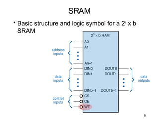

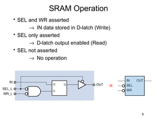
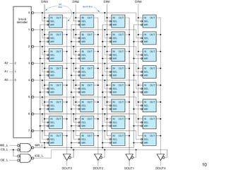
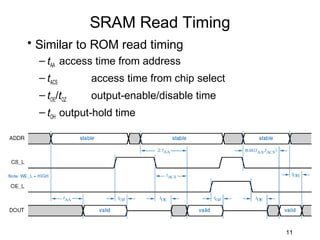
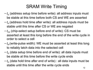
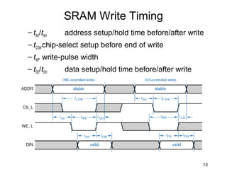
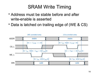
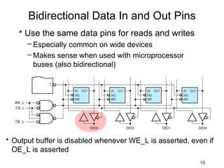
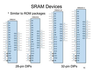
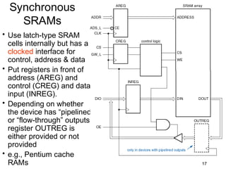


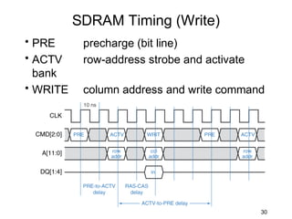
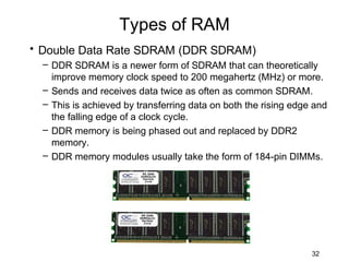

This document summarizes different types of random access memory (RAM), including static RAM (SRAM), dynamic RAM (DRAM), synchronous DRAM (SDRAM), and double data rate SDRAM (DDR SDRAM). It describes the basic operation and characteristics of each type of RAM, such as the use of transistors and capacitors, refresh requirements, packaging, and timing. Key details covered include the differences between SRAM and DRAM, DRAM refresh requirements, DRAM and SDRAM timing diagrams, and how DDR SDRAM transfers data on both clock edges.