Downloaded 109 times


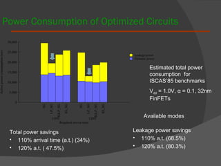


1. FinFETs allow for independent control of transistor gates, enabling new low-power circuit techniques like unusual logic styles and dual-Vdd circuits. 2. Simulation shows these FinFET circuit techniques can reduce total power consumption in ISCAS'85 benchmarks by up to 80% compared to traditional static CMOS designs. 3. FinFETs also enable architectural optimizations like variation-tolerant SRAM and novel non-volatile reconfigurable logic that could provide over an order of magnitude improvements in density and performance.