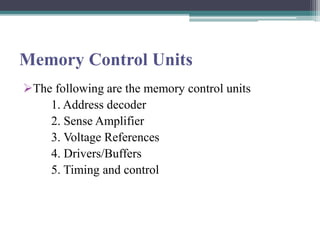
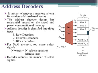
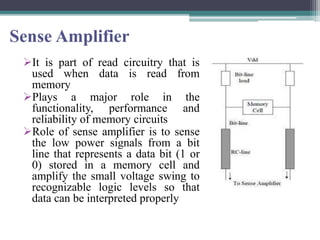
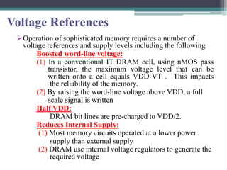
Academic Year 2017-18
EC6601 VLSI Design
Memory Circuits
Mrs.R.Chitra, AP/ECE,
Ramco Institute of Technology,
Rajapalayam.
Memory Control Units
The following are the memory control units
1. Address decoder
2. Sense Amplifier
3. Voltage References
4. Drivers/Buffers
5. Timing and control
Address Decoders
 It present whenever a memory allows
for random address-based access.
This address decoder design has
substantial impact on the speed and
power consumption of memory.
Address decoder is classified into three
types
1. Row Decoders
2. Column Decoders
3. Block decoders
For NxM memory, too many select
signals
N words = 'N' select signals or
address lines
Decoder reduces the number of select
signals.
M bits
A0
A1
AK2 1
K 5 log2N
Word 0
Word 1
Word 2
Word N2 2
Word N2 1
Storage
cell
S0
Input-Output
(M bits)
De
co
der
Sense Amplifier
It is part of read circuitry that is
used when data is read from
memory
Plays a major role in the
functionality, performance and
reliability of memory circuits
Role of sense amplifier is to sense
the low power signals from a bit
line that represents a data bit (1 or
0) stored in a memory cell and
amplify the small voltage swing to
recognizable logic levels so that
data can be interpreted properly
Voltage References
Operation of sophisticated memory requires a number of
voltage references and supply levels including the following
Boosted word-line voltage:
(1) In a conventional IT DRAM cell, using nMOS pass
transistor, the maximum voltage level that can be
written onto a cell equals VDD-VT . This impacts
the reliability of the memory.
(2) By raising the word-line voltage above VDD, a full
scale signal is written
Half VDD:
DRAM bit lines are pre-charged to VDD/2.
Reduces Internal Supply:
(1) Most memory circuits operated at a lower power
supply than external supply
(2) DRAM use internal voltage regulators to generate the
required voltage
Drivers/Buffers
Length of word and bit line increases with
increasing memory sizes
A major part of memory-periphery area is
allocated to the drivers, in particular the address
buffers and I/O drivers
Timing and Control
To achieve maximum performance, careful
timing is needed
Timing and control circuitry occupies a minimal
amount of area
Its design is an integral part and major part of
memory design process
Low Power Memory Circuits
 Reduction of power dissipation in
memories is becoming importance
 Memory designers have been remarkably
good in keeping power dissipation in check,
even while increasing the memory capacity
Source of power dissipation in memories
Power consumption in a memory chip is
attributed to the following three major sources.
1. Memory cell array
2. Decoders (row, column, block)
3. Periphery
IDD = Iarray+Idecoder+Iperiphery
= [miact+m(n-1)ihld]+[(n+m)CDE VINT f] +
[CPTVINTf+IDCP]
Contd…
Power dissipation is proportional to the size of
the memory (n,m)
Active power dissipation of the peripheral
circuits is small compared with other
components
However, standby power will be high
Partitioning of the memory
Proper memory division in sub modules give
active power dissipation to limited areas of the
overall memory
Memory units that are not in use should
consume only power necessary for data
retention
Memory units partitioning is accomplished by
reducing m and/or n
Contd…
By dividing word line into several sub-word-
lines that are enabled only when addressed, the
overall switched capacitance per access is
reduced
Partitioning of bit line reduces the capacitance
switched at every read/write operation
Addressing the Active Power Dissipation
Reducing the voltage levels is one of the most
effectively techniques to reduce power
dissipation.
SRAM Active Power Reduction
To obtain a fast read operation, the voltage swing
on the bit line is made between 0.1 and 0.3V
Resulting signal is transmitted to the sense
amplifier for restoration
A current flows through the bit line as long as the
word line is activated (∆t)
Limiting ∆t and bit line swing helps to keep the
active dissipation of SRAM low
In write operation, core voltage is reduced for power
reduction
Reducing supply voltage also impacts the memory
access time
DRAM Active Power Reduction
 Active readout process of a DRAM cell necessitates
successive operations of readout, amplification and
restoration for the selected cells
The bit lines are charges and discharged over the full
voltage swing for every read operation
Care should be given to reduce the bit line
dissipation charge
Voltage reduction has to be accompanied by either
an increase in the size of the storage capacitor.
The following techniques are quite effective
Contd…
Half VDD Precharge: Precharging the bit lines to
VDD /2 to reduce active
power dissipation in
DRAM
Boosted word line: raising the value of word
line above VDD during a
write operation eliminate
threshold drop over
access transistor increase in
stored charge
Contd…
Increased Capacitance area or value:
vertical capacitors used are very
effective in increasing the capacitance value
reduces voltage across capacitor C
Increased the cell size:
ultra-low voltage DRAM memory
operation require reduced area especially for
memories used in SOC
Data Retention Dissipation –
Data Retention in SRAM
In principle, SRAM array should not have any
static power dissipation. Yet, leakage current of
cell transistors is becoming a major source of
retention current
1. Turning off unused memory blocks
2. Increasing the threshold by using body
biasing
3. Inserting extra resistance in leakage path
4. Lowering the supply voltage
Data Retention in DRAM
Standby power in DRAMs is attributed to leakage
DRAM has to be refreshed continuously when in
data-retention mode
Refresh operation is performed by reading the m-
cells connected to a word line and restoring them
Standby power is proportional to bit line dissipation
charge and refresh frequency
Contd…
Leakage minimization in DRAM memories is VT
control and is accomplished at design time
One option to reduce leakage through the access
transistor in the DRAM cell is to turn OFF the
device hard by applying a negative voltage to the
word lines of non-active cells
References:
• Jan Rabaey, Anantha Chandrakasan, B.Nikolic,
“Digital Integrated Circuits: A Design Perspective”,
Second Edition, Prentice Hall of India, 2003.
• M.J. Smith, “Application Specific Integrated
Circuits”, Addisson Wesley, 1997.
• N.Weste, K.Eshraghian, “Principles of CMOS VLSI
Design”, Second Edition, Addision Wesley 1993.

EC6601 VLSI Design Memory Circuits

  • 1.
    Academic Year 2017-18 EC6601VLSI Design Memory Circuits Mrs.R.Chitra, AP/ECE, Ramco Institute of Technology, Rajapalayam.
  • 2.
    Memory Control Units Thefollowing are the memory control units 1. Address decoder 2. Sense Amplifier 3. Voltage References 4. Drivers/Buffers 5. Timing and control
  • 3.
    Address Decoders  Itpresent whenever a memory allows for random address-based access. This address decoder design has substantial impact on the speed and power consumption of memory. Address decoder is classified into three types 1. Row Decoders 2. Column Decoders 3. Block decoders For NxM memory, too many select signals N words = 'N' select signals or address lines Decoder reduces the number of select signals. M bits A0 A1 AK2 1 K 5 log2N Word 0 Word 1 Word 2 Word N2 2 Word N2 1 Storage cell S0 Input-Output (M bits) De co der
  • 4.
    Sense Amplifier It ispart of read circuitry that is used when data is read from memory Plays a major role in the functionality, performance and reliability of memory circuits Role of sense amplifier is to sense the low power signals from a bit line that represents a data bit (1 or 0) stored in a memory cell and amplify the small voltage swing to recognizable logic levels so that data can be interpreted properly
  • 5.
    Voltage References Operation ofsophisticated memory requires a number of voltage references and supply levels including the following Boosted word-line voltage: (1) In a conventional IT DRAM cell, using nMOS pass transistor, the maximum voltage level that can be written onto a cell equals VDD-VT . This impacts the reliability of the memory. (2) By raising the word-line voltage above VDD, a full scale signal is written Half VDD: DRAM bit lines are pre-charged to VDD/2. Reduces Internal Supply: (1) Most memory circuits operated at a lower power supply than external supply (2) DRAM use internal voltage regulators to generate the required voltage
  • 6.
    Drivers/Buffers Length of wordand bit line increases with increasing memory sizes A major part of memory-periphery area is allocated to the drivers, in particular the address buffers and I/O drivers
  • 7.
    Timing and Control Toachieve maximum performance, careful timing is needed Timing and control circuitry occupies a minimal amount of area Its design is an integral part and major part of memory design process
  • 8.
    Low Power MemoryCircuits  Reduction of power dissipation in memories is becoming importance  Memory designers have been remarkably good in keeping power dissipation in check, even while increasing the memory capacity
  • 9.
    Source of powerdissipation in memories Power consumption in a memory chip is attributed to the following three major sources. 1. Memory cell array 2. Decoders (row, column, block) 3. Periphery
  • 10.
    IDD = Iarray+Idecoder+Iperiphery =[miact+m(n-1)ihld]+[(n+m)CDE VINT f] + [CPTVINTf+IDCP]
  • 11.
    Contd… Power dissipation isproportional to the size of the memory (n,m) Active power dissipation of the peripheral circuits is small compared with other components However, standby power will be high
  • 12.
    Partitioning of thememory Proper memory division in sub modules give active power dissipation to limited areas of the overall memory Memory units that are not in use should consume only power necessary for data retention Memory units partitioning is accomplished by reducing m and/or n
  • 13.
    Contd… By dividing wordline into several sub-word- lines that are enabled only when addressed, the overall switched capacitance per access is reduced Partitioning of bit line reduces the capacitance switched at every read/write operation
  • 14.
    Addressing the ActivePower Dissipation Reducing the voltage levels is one of the most effectively techniques to reduce power dissipation.
  • 15.
    SRAM Active PowerReduction To obtain a fast read operation, the voltage swing on the bit line is made between 0.1 and 0.3V Resulting signal is transmitted to the sense amplifier for restoration A current flows through the bit line as long as the word line is activated (∆t) Limiting ∆t and bit line swing helps to keep the active dissipation of SRAM low In write operation, core voltage is reduced for power reduction Reducing supply voltage also impacts the memory access time
  • 16.
    DRAM Active PowerReduction  Active readout process of a DRAM cell necessitates successive operations of readout, amplification and restoration for the selected cells The bit lines are charges and discharged over the full voltage swing for every read operation Care should be given to reduce the bit line dissipation charge Voltage reduction has to be accompanied by either an increase in the size of the storage capacitor. The following techniques are quite effective
  • 17.
    Contd… Half VDD Precharge:Precharging the bit lines to VDD /2 to reduce active power dissipation in DRAM Boosted word line: raising the value of word line above VDD during a write operation eliminate threshold drop over access transistor increase in stored charge
  • 18.
    Contd… Increased Capacitance areaor value: vertical capacitors used are very effective in increasing the capacitance value reduces voltage across capacitor C Increased the cell size: ultra-low voltage DRAM memory operation require reduced area especially for memories used in SOC
  • 19.
    Data Retention Dissipation– Data Retention in SRAM In principle, SRAM array should not have any static power dissipation. Yet, leakage current of cell transistors is becoming a major source of retention current 1. Turning off unused memory blocks 2. Increasing the threshold by using body biasing 3. Inserting extra resistance in leakage path 4. Lowering the supply voltage
  • 20.
    Data Retention inDRAM Standby power in DRAMs is attributed to leakage DRAM has to be refreshed continuously when in data-retention mode Refresh operation is performed by reading the m- cells connected to a word line and restoring them Standby power is proportional to bit line dissipation charge and refresh frequency
  • 21.
    Contd… Leakage minimization inDRAM memories is VT control and is accomplished at design time One option to reduce leakage through the access transistor in the DRAM cell is to turn OFF the device hard by applying a negative voltage to the word lines of non-active cells
  • 22.
    References: • Jan Rabaey,Anantha Chandrakasan, B.Nikolic, “Digital Integrated Circuits: A Design Perspective”, Second Edition, Prentice Hall of India, 2003. • M.J. Smith, “Application Specific Integrated Circuits”, Addisson Wesley, 1997. • N.Weste, K.Eshraghian, “Principles of CMOS VLSI Design”, Second Edition, Addision Wesley 1993.