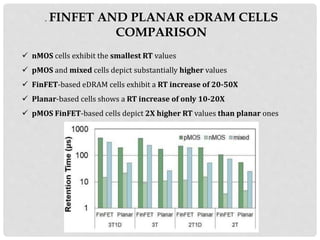
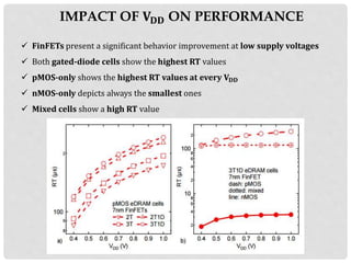
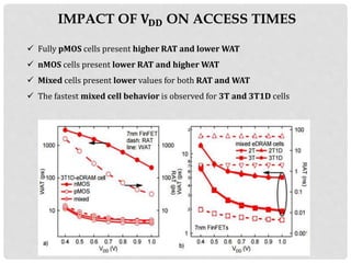
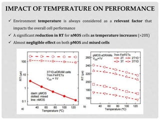
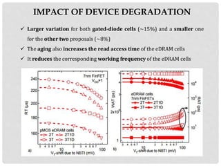
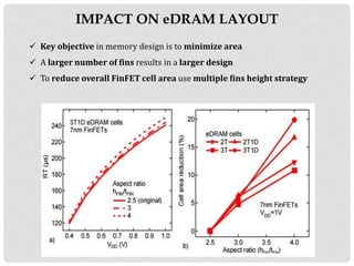
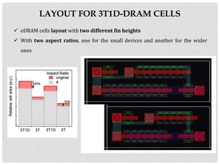
EMBEDDED DRAM CELLS
USING FINFET TECHNOLOGY
CONTENTS
 INTRODUCTION
 WHY FinFET AND FIN DESIGN CONSIDERATIONS
 RELIABILITY ISSUES
 eDRAM USING FinFET
 eDRAM CELL PARAMETERS
 FINFET AND PLANAR eDRAM CELLS COMPARISON
 IMPACT OF 𝐕 𝐃𝐃 ON PERFORMANCE AND ACCESS TIMES
 IMPACT OF TEMPERATURE ON PERFORMANCE
 IMPACT OF DEVICE DEGRADATION
 IMPACT ON eDRAM LAYOUT
 CONCLUSION
 REFERENCES
INTRODUCTION
 FinFET is a MOSFET whose body is a thin piece of silicon with gates
above and below it
 The distinguishing characteristic of the FinFET is that the conducting
channel is wrapped by a thin silicon "fin", which forms the body of the
device
WHY FINFET?
 As the gate length shrinks, the MOSFET’s Id-Vg characteristics degrade in two
major ways:
♦ Subthreshold swing (S) degrades and Threshold voltage (𝑉𝑡)
decreases
♦ S and 𝑉𝑡 become increasingly sensitive to Gate length (𝐿 𝑔)
variations
short-channel
effect
 MOSFET becomes “resistor” at small L
 Gate cannot control the leakage current
paths that are far from the gate
IDSAT ∝ (VDD - VT)η 1 < η < 2
FIN DESIGN CONSIDERATIONS
 Fin Width
– Determines DIBL
 Fin Height
– Limited by etch technology
– Trade-off: layout efficiency vs. design flexibility
 Fin Pitch
– Determines layout area
– Limits S/D implant tilt angle
– Trade-off: performance vs. layout efficiency
RELIABILITY ISSUES
 Self-heating
 Device degradation
 Bias Temperature Instability (BTI)
 Larger layout area
eDRAM USING FinFET
 eDRAMs are promising memory cells to substitute static memories
 eDRAMs can achieve:
♦ higher densities(2X)
♦ smaller cell leakage current
2T 2T1D
3T 3T1D
eDRAM CELL PARAMETERS
 Retention Time (RT): It is the time required for the storage node voltage
(VS) in the cell to decay to VSmin
 Write Access Time (WAT): It is defined as the time elapsed between
V(WLwrite)=(0.5*VDD) and VS=(0.9*(VDD-VT))
 Read Access Time (RAT): It is defined as the time elapsed between
V(WLwrite)=(0.5*VDD) and V(BLread)=(0.9*VDD)
. FINFET AND PLANAR eDRAM CELLS
COMPARISON
 nMOS cells exhibit the smallest RT values
 pMOS and mixed cells depict substantially higher values
 FinFET-based eDRAM cells exhibit a RT increase of 20-50X
 Planar-based cells shows a RT increase of only 10-20X
 pMOS FinFET-based cells depict 2X higher RT values than planar ones
IMPACT OF 𝐕 𝐃𝐃 ON PERFORMANCE
 FinFETs present a significant behavior improvement at low supply voltages
 Both gated-diode cells show the highest RT values
 pMOS-only shows the highest RT values at every 𝐕 𝐃𝐃
 nMOS-only depicts always the smallest ones
 Mixed cells show a high RT value
IMPACT OF 𝐕 𝐃𝐃 ON ACCESS TIMES
 Fully pMOS cells present higher RAT and lower WAT
 nMOS cells present lower RAT and higher WAT
 Mixed cells present lower values for both RAT and WAT
 The fastest mixed cell behavior is observed for 3T and 3T1D cells
IMPACT OF TEMPERATURE ON PERFORMANCE
 Environment temperature is always considered as a relevant factor that
impacts the overall cell performance
 A significant reduction in RT for nMOS cells as temperature increases (>20X)
 Almost negligible effect on both pMOS and mixed cells
IMPACT OF DEVICE DEGRADATION
 Larger variation for both gated-diode cells (~15%) and a smaller one
for the other two proposals (~8%)
 The aging also increases the read access time of the eDRAM cells
 It reduces the corresponding working frequency of the eDRAM cells
IMPACT ON eDRAM LAYOUT
 Key objective in memory design is to minimize area
 A larger number of fins results in a larger design
 To reduce overall FinFET cell area use multiple fins height strategy
LAYOUT FOR 3T1D-DRAM CELLS
 eDRAM cells layout with two different fin heights
 With two aspect ratios, one for the small devices and another for the wider
ones
CONCLUSION
 FinFETs avoid problems faced by conventional MOSFETs such as subthreshold
swing degradation and leakage
 The eDRAM cells based on multiple-gate devices show a 2X improvement of
the retention time
 The eDRAM cells fully based on pMOS FinFETs achieve the largest retention
time values, under low VDD and high temperature
 FinFETs are very promising candidate for future nano-scale CMOS technology
and high-density memory application
REFERENCES
1. K. J. Kuhn, “CMOS scaling for the 22nm node and beyond: Device physics and
technology,” in Proceedings of the International Symposium on VLSI Technology,
Systems and Applications (VLSI-TSA ’11), pp. 1–2, April 2011.
2. N. Bhoj and N. K. Jha, “Gated-diode FinFET DRAMs: Device and circuit design-
considerations,” J. Emerg. Technol. Comput. Syst., vol. 6, no. 4, pp. 12:1– 12:32,
2010.
3. Xinyun Xie, “14nm FinFET device electronic study”, China Semiconductor
Technology International Conference (CSTIC), pp. 1-3, 2016.
4. Kai-Lin Lee ; Ren-Yu He ; Hung-Wen Huang ; Chih-Chieh Yeh, “A study of fin width
effect on the performance of FinFET”, IEEE 22nd International Symposium on the
Physical and Failure Analysis of Integrated Circuits, pp. 503 – 504, 2015.
THANK YOU

eDRAM Cells using FinFET Technology

  • 1.
    EMBEDDED DRAM CELLS USINGFINFET TECHNOLOGY
  • 2.
    CONTENTS  INTRODUCTION  WHYFinFET AND FIN DESIGN CONSIDERATIONS  RELIABILITY ISSUES  eDRAM USING FinFET  eDRAM CELL PARAMETERS  FINFET AND PLANAR eDRAM CELLS COMPARISON  IMPACT OF 𝐕 𝐃𝐃 ON PERFORMANCE AND ACCESS TIMES  IMPACT OF TEMPERATURE ON PERFORMANCE  IMPACT OF DEVICE DEGRADATION  IMPACT ON eDRAM LAYOUT  CONCLUSION  REFERENCES
  • 3.
    INTRODUCTION  FinFET isa MOSFET whose body is a thin piece of silicon with gates above and below it  The distinguishing characteristic of the FinFET is that the conducting channel is wrapped by a thin silicon "fin", which forms the body of the device
  • 4.
    WHY FINFET?  Asthe gate length shrinks, the MOSFET’s Id-Vg characteristics degrade in two major ways: ♦ Subthreshold swing (S) degrades and Threshold voltage (𝑉𝑡) decreases ♦ S and 𝑉𝑡 become increasingly sensitive to Gate length (𝐿 𝑔) variations short-channel effect  MOSFET becomes “resistor” at small L  Gate cannot control the leakage current paths that are far from the gate IDSAT ∝ (VDD - VT)η 1 < η < 2
  • 5.
    FIN DESIGN CONSIDERATIONS Fin Width – Determines DIBL  Fin Height – Limited by etch technology – Trade-off: layout efficiency vs. design flexibility  Fin Pitch – Determines layout area – Limits S/D implant tilt angle – Trade-off: performance vs. layout efficiency
  • 6.
    RELIABILITY ISSUES  Self-heating Device degradation  Bias Temperature Instability (BTI)  Larger layout area
  • 7.
    eDRAM USING FinFET eDRAMs are promising memory cells to substitute static memories  eDRAMs can achieve: ♦ higher densities(2X) ♦ smaller cell leakage current 2T 2T1D 3T 3T1D
  • 8.
    eDRAM CELL PARAMETERS Retention Time (RT): It is the time required for the storage node voltage (VS) in the cell to decay to VSmin  Write Access Time (WAT): It is defined as the time elapsed between V(WLwrite)=(0.5*VDD) and VS=(0.9*(VDD-VT))  Read Access Time (RAT): It is defined as the time elapsed between V(WLwrite)=(0.5*VDD) and V(BLread)=(0.9*VDD)
  • 9.
    . FINFET ANDPLANAR eDRAM CELLS COMPARISON  nMOS cells exhibit the smallest RT values  pMOS and mixed cells depict substantially higher values  FinFET-based eDRAM cells exhibit a RT increase of 20-50X  Planar-based cells shows a RT increase of only 10-20X  pMOS FinFET-based cells depict 2X higher RT values than planar ones
  • 10.
    IMPACT OF 𝐕𝐃𝐃 ON PERFORMANCE  FinFETs present a significant behavior improvement at low supply voltages  Both gated-diode cells show the highest RT values  pMOS-only shows the highest RT values at every 𝐕 𝐃𝐃  nMOS-only depicts always the smallest ones  Mixed cells show a high RT value
  • 11.
    IMPACT OF 𝐕𝐃𝐃 ON ACCESS TIMES  Fully pMOS cells present higher RAT and lower WAT  nMOS cells present lower RAT and higher WAT  Mixed cells present lower values for both RAT and WAT  The fastest mixed cell behavior is observed for 3T and 3T1D cells
  • 12.
    IMPACT OF TEMPERATUREON PERFORMANCE  Environment temperature is always considered as a relevant factor that impacts the overall cell performance  A significant reduction in RT for nMOS cells as temperature increases (>20X)  Almost negligible effect on both pMOS and mixed cells
  • 13.
    IMPACT OF DEVICEDEGRADATION  Larger variation for both gated-diode cells (~15%) and a smaller one for the other two proposals (~8%)  The aging also increases the read access time of the eDRAM cells  It reduces the corresponding working frequency of the eDRAM cells
  • 14.
    IMPACT ON eDRAMLAYOUT  Key objective in memory design is to minimize area  A larger number of fins results in a larger design  To reduce overall FinFET cell area use multiple fins height strategy
  • 15.
    LAYOUT FOR 3T1D-DRAMCELLS  eDRAM cells layout with two different fin heights  With two aspect ratios, one for the small devices and another for the wider ones
  • 16.
    CONCLUSION  FinFETs avoidproblems faced by conventional MOSFETs such as subthreshold swing degradation and leakage  The eDRAM cells based on multiple-gate devices show a 2X improvement of the retention time  The eDRAM cells fully based on pMOS FinFETs achieve the largest retention time values, under low VDD and high temperature  FinFETs are very promising candidate for future nano-scale CMOS technology and high-density memory application
  • 17.
    REFERENCES 1. K. J.Kuhn, “CMOS scaling for the 22nm node and beyond: Device physics and technology,” in Proceedings of the International Symposium on VLSI Technology, Systems and Applications (VLSI-TSA ’11), pp. 1–2, April 2011. 2. N. Bhoj and N. K. Jha, “Gated-diode FinFET DRAMs: Device and circuit design- considerations,” J. Emerg. Technol. Comput. Syst., vol. 6, no. 4, pp. 12:1– 12:32, 2010. 3. Xinyun Xie, “14nm FinFET device electronic study”, China Semiconductor Technology International Conference (CSTIC), pp. 1-3, 2016. 4. Kai-Lin Lee ; Ren-Yu He ; Hung-Wen Huang ; Chih-Chieh Yeh, “A study of fin width effect on the performance of FinFET”, IEEE 22nd International Symposium on the Physical and Failure Analysis of Integrated Circuits, pp. 503 – 504, 2015.
  • 18.