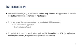
This document provides an overview of phase locked loops (PLL) including:
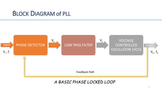
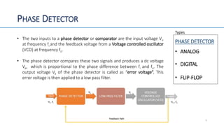
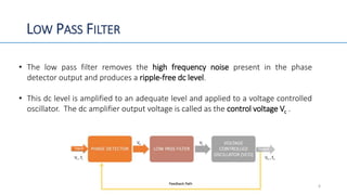
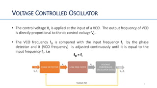
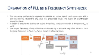
1. The basic components of a PLL including a phase detector, low pass filter, and voltage controlled oscillator that work together in a closed loop to lock the output frequency and phase to the input signal.
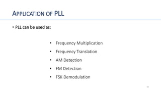
2. Examples of PLL applications such as frequency multiplication, FM demodulation, and motor speed control.
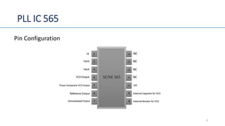
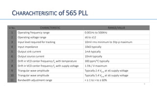
3. A more detailed description of the 565 PLL IC including its pin configuration and characteristics such as operating frequency range and drift with temperature/voltage.