Downloaded 1,067 times


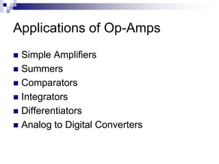

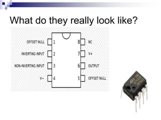
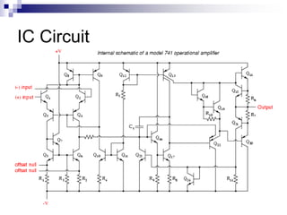
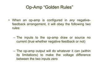
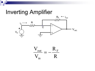
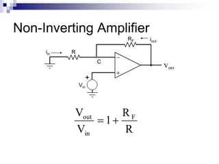
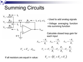


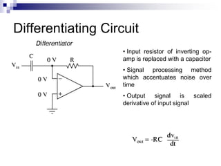


An operational amplifier (op-amp) is an integrated circuit that can amplify or compare signals. It consists of transistors, resistors, and capacitors. Op-amps are used to build amplifiers, summers, integrators, differentiators, and comparators. They obey golden rules to make the difference between their input pins zero. Op-amps are also used in analog to digital converters, which sample analog signals and convert them to digital signals for processing.


