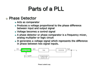
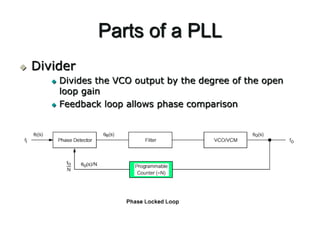
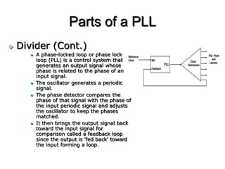
A PLL consists of a phase detector, filter, voltage controlled oscillator (VCO), and optional divider. The phase detector compares the phase of the input signal to the VCO output signal and generates an error voltage. The filter smooths the error voltage which is fed to the VCO. The VCO then adjusts its output frequency according to the error voltage to minimize the phase difference between its output and the input signal. An optional divider may be included to scale the VCO output frequency before feeding it back to the phase detector for comparison to the input signal. In this way, the PLL is able to lock its output phase to the input phase or some multiple of the input phase.
THIS PPT IS GIVEN BY EC FINAL YEAR STUDENTS OF BCE-MANDIDEEP TO PROF. RAVITESH MISHRA ON CHARGED PUMP PLLS AS AN ASSIGNMENT FROM RAZAVI,DESIGN OF ANALOG CMOS INTEGRATED CIRCUITS
Originally presented at DesignCon 2013.
Jitter is a very important topic in signal integrity for high speed serial data links. The jitter performance of clock signals used in generating the serial data signal is critical to the overall performance of these signals.
Phase noise is the most sensitive and accurate measurement of the performance of precision clocks.
This presentation covers the theory and practice for making phase noise measurements on clock signals as well as the relationship between phase noise and total jitter, random jitter and deterministic jitter. Measurements on a typical clock signal is also included.
For more information, visit http://rohde-schwarz-scopes.com or call (888) 837-8772 to speak to a local Rohde & Schwarz expert.
In telecommunication, an eye pattern, also known as an eye diagram, is an oscilloscope display in which a digital signal from a receiver is repetitively sampled and applied to the vertical input, while the data rate is used to trigger the horizontal sweep. It is so called because, for several types of coding, the pattern looks like a series of eyes between a pair of rails. It is a tool for the evaluation of the combined effects of channel noise and intersymbol interference on the performance of a baseband pulse-transmission system. It is the synchronised superposition of all possible realisations of the signal of interest viewed within a particular signaling interval.
In communication system, intersymbol interference (ISI) is a form of distortion of a signal in which one symbol interferes with subsequent symbols. This is an unwanted phenomenon as the previous symbols have similar effect as noise, thus making the communication less reliable.
In communication system, the Nyquist ISI criterion describes the conditions which when satisfied by a communication channel (including responses of transmit and receive filters), result in no intersymbol interference(ISI). It provides a method for constructing band-limited functions to overcome the effects of intersymbol interference.
Salient Features:
The magnitude response is nearly constant(equal to 1) at lower frequencies
There are no ripples in passband and stop band
The maximum gain occurs at Ω=0 and it is H(Ω)=1
The magnitude response is monotonically decreasing
As the order of the filter ‘N’ increases, the response of the filter is more close to the ideal response
In this video, I will explain what is QAM modulation and what is 16QAM.
QAM Stands for Quadrature Amplitude Modulation. QAM is both an analog and a digital modulation method. But here, we are only talking about QAM as a digital modulation.
Quadrature means that two carrier waves are being used, one sine wave and one cosine wave. These two waves are out of phase with each other by 90°, this is called quadrature.
At the receiving end, the sine and cosine wave can be decoded independently, this means that by using both a sine wave and a cosine wave, the communication channel's capacity is doubled comparing to using only one sine or one cosine wave. That is why quadrature is such a popular technique for digital modulation.
QAM modulation is a combination of Amplitude Shift Keying and Phase Shift Keying, both carrier wave is modulated by changing both its amplitude and phase. As shown in this 8QAM waveform, the top is the sine wave carrier, for bit 000, the sin wave has a phase shift of 0°, and an amplitude of 2. While for bit 110, the phase shift is 180°, and the amplitude now is 1. So both phase and amplitude are changed.
In 16QAM, the input binary data is combined into groups of 4 bits called QUADBITS.
As shown in this picture, the I and I' bits are sent to the sine wave modulation path, and the Q and Q' bits are sent to the cosine wave path. Since the bits are split and sent in parallel, so the symbol rate has been reduced to a quarter of the input binary bit rate. If the input binary data rate is 100 Gbps, then the symbol rate is reduced to only 25 Gbaud/second. This is the reason why 16QAM is under hot research for 100Gbps fiber optic communication.
The I and Q bits control the carrier wave's phase shift, if the bit is 0, then the phase shift is 180°, if the bit is 1, then the phase shift is 0°.
The I' and Q' bits control the carrier wave's amplitude, if bit is 0, then the amplitude is 0.22 volt, if the bit is 1, then the amplitude is 0.821 volt.
So each pair of bits has 4 different outputs. Then they are added up at the linear summer. 4X4 is 16, so there is a total of 16 different combinations at the output, that is why this is called 16QAM.
This illustration shows an example of how the QUADBIT 0000 is modulated onto the carrier waves.
Here I and I' is 00, so the output is -0.22 Volt at the 2-to-4-level converter, when timed with the sine wave carrier, we get -0.22sin(2πfct), here fc is the carrier wave's frequency. QQ' is also 00, so the other carrier wave output is -0.22cos(2πfct).
Here is the proof that quadbit 0000 is modulated as a sine wave with an amplitude of 0.311volt and a phase shift of -135°. You can now pause for a moment to study the proof.
This list shows the 16QAM modulation output with different amplitude and phase change for all 16 quadbits. On the right side is the constellation diagram which shows the positions of these quadbits on a I-Q diagram.
You can visit FO4SALE.com f
Phase Locked Loop with Filter Banks for High Data Rate Satellite Linkchiragwarty
Satellite communication systems operate in the
presence of path loss and atmospherically induced fading,
which results in waveform distortion, altering phase and bit
time period. After penetrating through several atmospheric
layers, the signal experiences Doppler shift which results in
frequency change and phase reversal, thus to sync the
receiver to the incoming signal we make use of the Phase
Locked Loop (PLL) with a filter at its core functioning.
To recover and reconstruct the original signal, the use of
filter banks in the loop filter block of the PLL will be added
and discussed. The idea of using M-channel uniform filter
banks is to minimize the error by optimizing the
performance in decomposition and reconstruction of signals.
Using different types of fundamental coherent digital
modulation schemes like, M-ary Amplitude/Frequency
/Phase shift keying (MASK, MFSK, MPSK), the best
optimized solution can be determined for all M-channels for
high data rates and bandwidth constraints.
The presentation studies the design of a digital PLL system by
using a variable filter block for several digital modulation
schemes used in ground to space communication links. Two
basic designs will be developed, first model with a fixed set
of filters, those seen in traditional legacy systems and the
second model, which consist of a filtering block made up of
Quadrature Mirror Filter banks (QMF). The method is based
on the strength of the incoming signal and modulation
scheme, which in turn decides the number of filter banks, to
be used to recover the signal.
In this presentation, the focus on pseudo-adaptive nature of the
filter banks is to reconstruct the original signal, considering
the effects of Doppler shift for fast moving airborne
platforms. Subsequently, the comparison between the
performance of the fixed filter based architecture and the
additional design with the variable pseudo-adaptive filter
banks design includes the QMF and Discrete Cosine
Transform Filter banks (DCT). This will follow with the
software oriented simulation of the performance of the
proposed design method, in different scenarios experienced
in satellite links.
Optimization of Digitally Controlled Oscillator with Low Poweriosrjce
IOSR journal of VLSI and Signal Processing (IOSRJVSP) is a double blind peer reviewed International Journal that publishes articles which contribute new results in all areas of VLSI Design & Signal Processing. The goal of this journal is to bring together researchers and practitioners from academia and industry to focus on advanced VLSI Design & Signal Processing concepts and establishing new collaborations in these areas.
Design and realization of microelectronic systems using VLSI/ULSI technologies require close collaboration among scientists and engineers in the fields of systems architecture, logic and circuit design, chips and wafer fabrication, packaging, testing and systems applications. Generation of specifications, design and verification must be performed at all abstraction levels, including the system, register-transfer, logic, circuit, transistor and process levels
What is PLL and elements of PLL??
What is Analog PLL??
What is Digital PLL??
What are the components of Digital PLL??
Applications of PLL
PLL as 565 IC pin diagram
PLL as Frequency Synthesizer (Frequency Translator)
PLL as Frequency Division
PLL as Frequency Multiplication
PLL as FM Demodulator
IJERA (International journal of Engineering Research and Applications) is International online, ... peer reviewed journal. For more detail or submit your article, please visit www.ijera.com
This section discusses the most
important PLL conept, block diagram , fucntions and gives guidelines for the design of these circuits. It discuss the Monolithic PLL IC, centre frequency.
Student information management system project report ii.pdfKamal Acharya
Our project explains about the student management. This project mainly explains the various actions related to student details. This project shows some ease in adding, editing and deleting the student details. It also provides a less time consuming process for viewing, adding, editing and deleting the marks of the students.
Welcome to WIPAC Monthly the magazine brought to you by the LinkedIn Group Water Industry Process Automation & Control.
In this month's edition, along with this month's industry news to celebrate the 13 years since the group was created we have articles including
A case study of the used of Advanced Process Control at the Wastewater Treatment works at Lleida in Spain
A look back on an article on smart wastewater networks in order to see how the industry has measured up in the interim around the adoption of Digital Transformation in the Water Industry.
Water scarcity is the lack of fresh water resources to meet the standard water demand. There are two type of water scarcity. One is physical. The other is economic water scarcity.
2. What is a PLL?
Digital frequency control system
Generate high speed oscillations
Acquire and track signals
• Radio Frequency Demodulation
• DX-ing
• RF communications
6. Parts of a PLL
Phase Detector
Filter
Voltage Controlled Oscillator
Programmable Counter
7. Parts of a PLL
Phase Detector
Acts as comparator
Produces a voltage proportional to the phase difference
between input and output signal
Voltage becomes a control signal
A phase detector or phase comparator is a frequency mixer,
analog multiplier or logic circuit
It generates a voltage signal which represents the difference
in phase between two signal inputs.
8. Parts of a PLL
Filter
Determines dynamic characteristics of PLL
Specify Capture Range (bandwidth)
Specify Tracking Range
Receives signal from Phase Detector and filters
accordingly
9. Parts of a PLL
Filter (Cont.)
It provides a smoother form of a signal, removing
the short-term fluctuations, and leaving the
longer-term trend.
PLL loop filter (usually a low pass filter) generally
has two distinct functions.
The primary function is to determine loop
dynamics, also called stability. This is how the
loop responds to disturbances, such as changes in
the reference frequency.
10. Parts of a PLL
Filter (Cont.)
The most common and
easily understood active
filter is the Active Low Pass
Filter.
It uses an op-amp for
amplification and gain
control.
The simplest form of a low
pass active filter is to
connect an inverting or non-inverting
amplifier.
The advantage of this
configuration is that the op-amps
high input impedance
prevents excessive loading
on the filters output .
11. Parts of a PLL
Voltage Controlled Oscillator
Changes a DC input voltage into a pulsed waveform.
The output frequency is proportional to the
magnitude of input control voltage.
Its output can be of any waveshape.
12. Parts of a PLL
Voltage Controlled Oscillator (Cont.)
The ouput frequency of a VCO is given by:
fout = fmin + KVCOVin
where fmin = output frequency when Vin=0
KVCO = VCO conversion gain, Hz/V
In PLL, the VCO output frequency (fo) is fed to one
input of the phase detector.
Phase detector compares it with the frequency of
input signal (fi) which is at its other input.
13. Parts of a PLL
Divider
Divides the VCO output by the degree of the open
loop gain
Feedback loop allows phase comparison
14. Parts of a PLL
Divider (Cont.)
A phase-locked loop or phase lock
loop (PLL) is a control system that
generates an output signal whose
phase is related to the phase of an
input signal.
The oscillator generates a periodic
signal.
The phase detector compares the
phase of that signal with the phase of
the input periodic signal and adjusts
the oscillator to keep the phases
matched.
It then brings the output signal back
toward the input signal for
comparison called a feedback loop
since the output is 'fed back' toward
the input forming a loop.