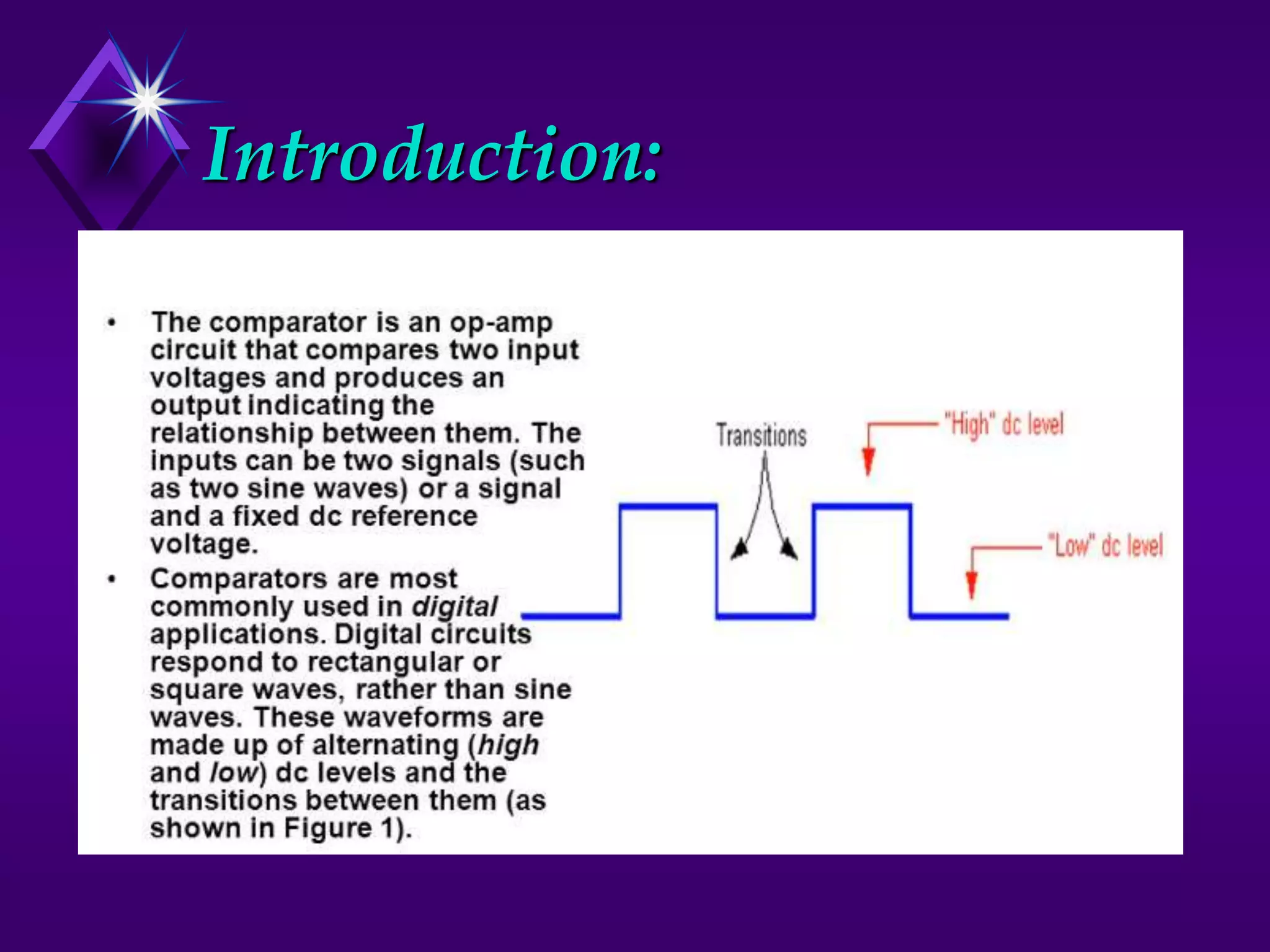
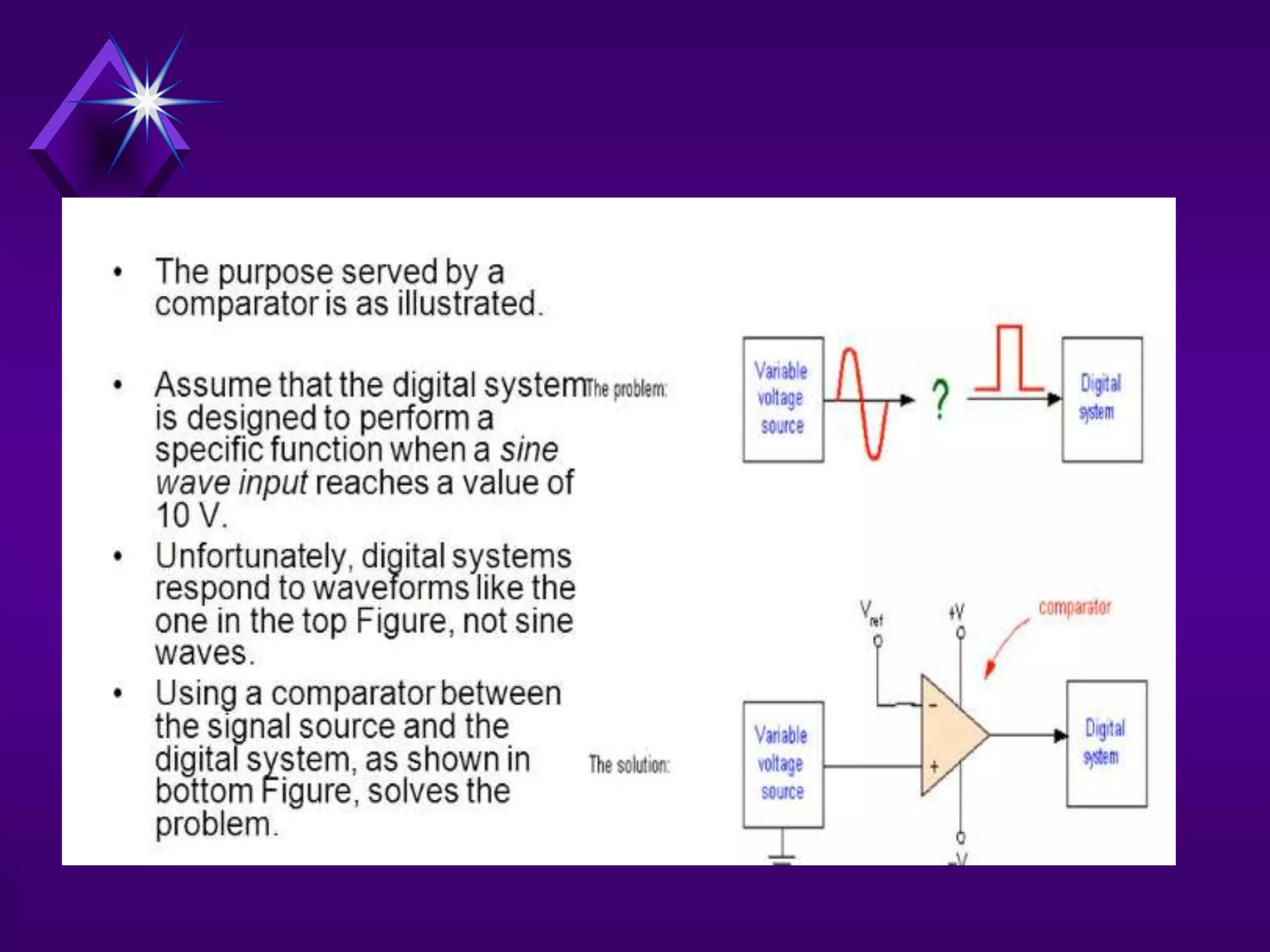
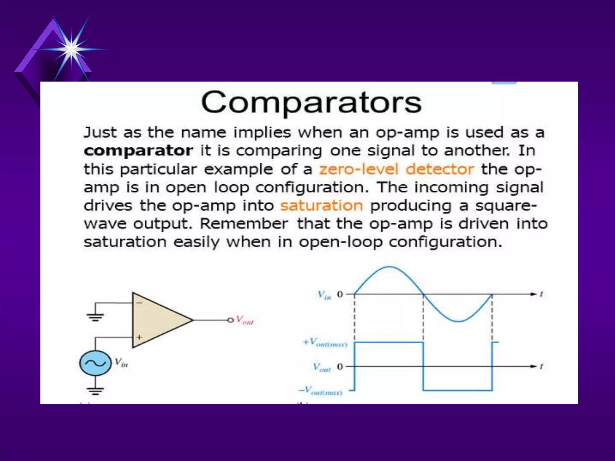
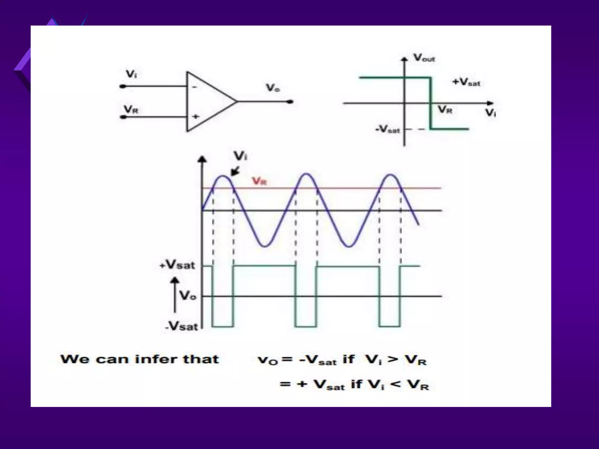
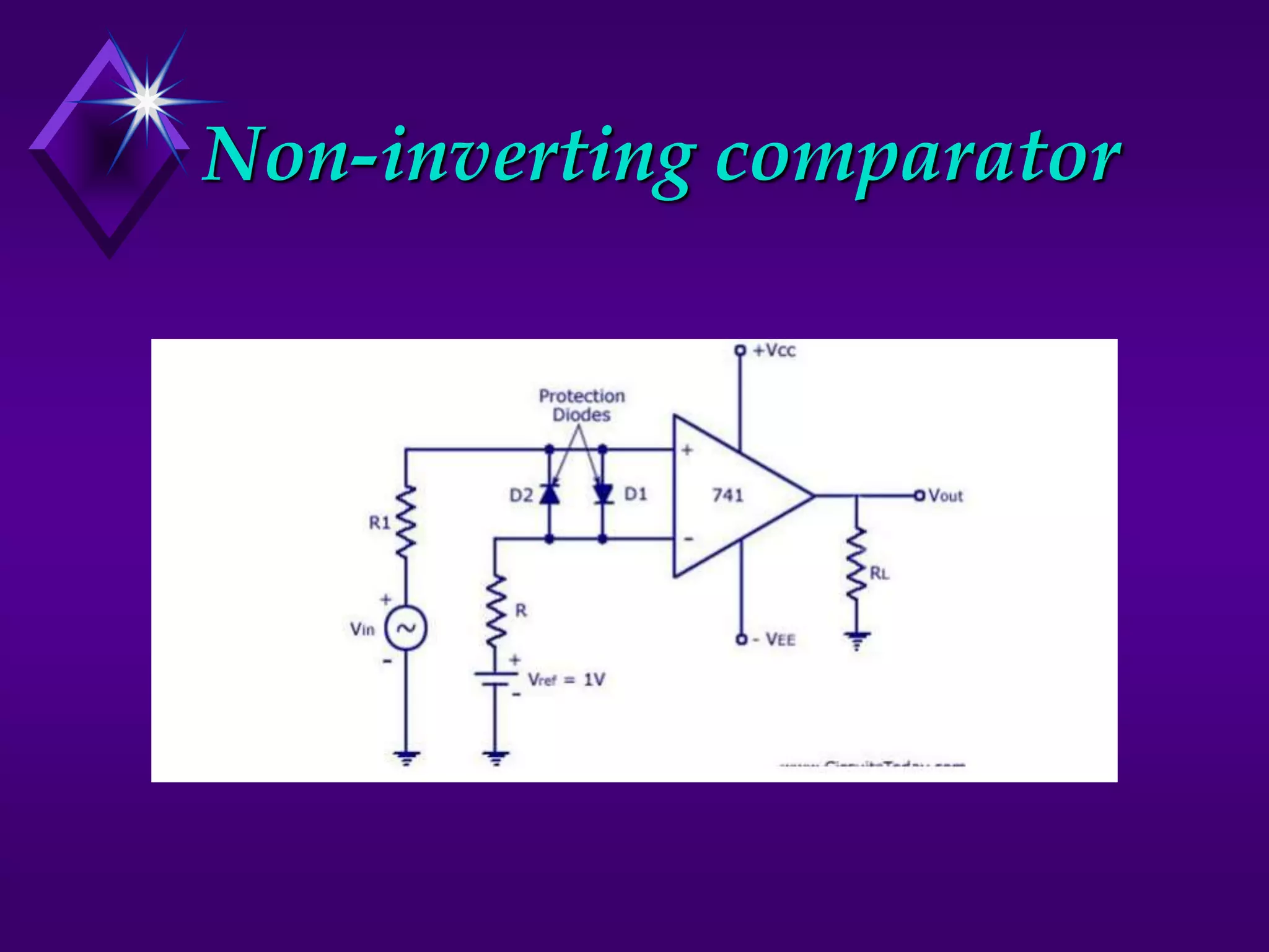
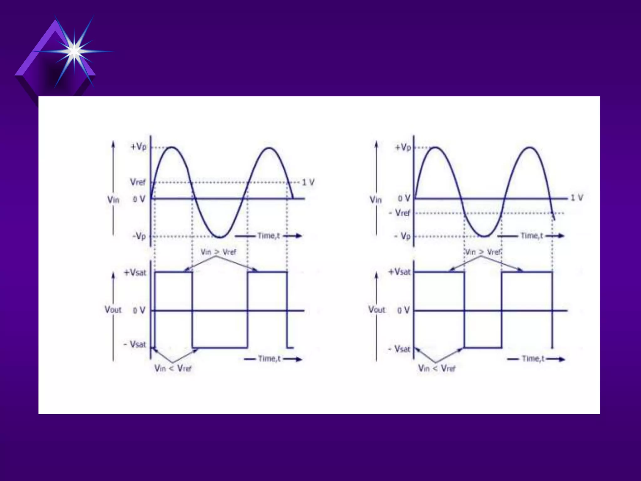
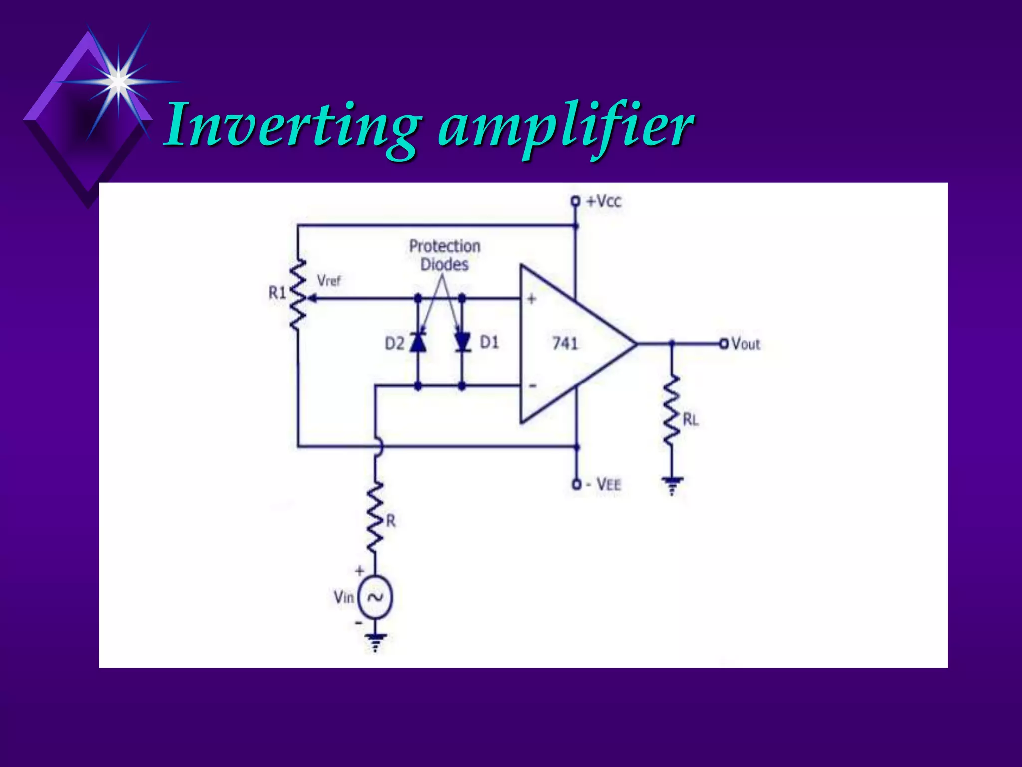
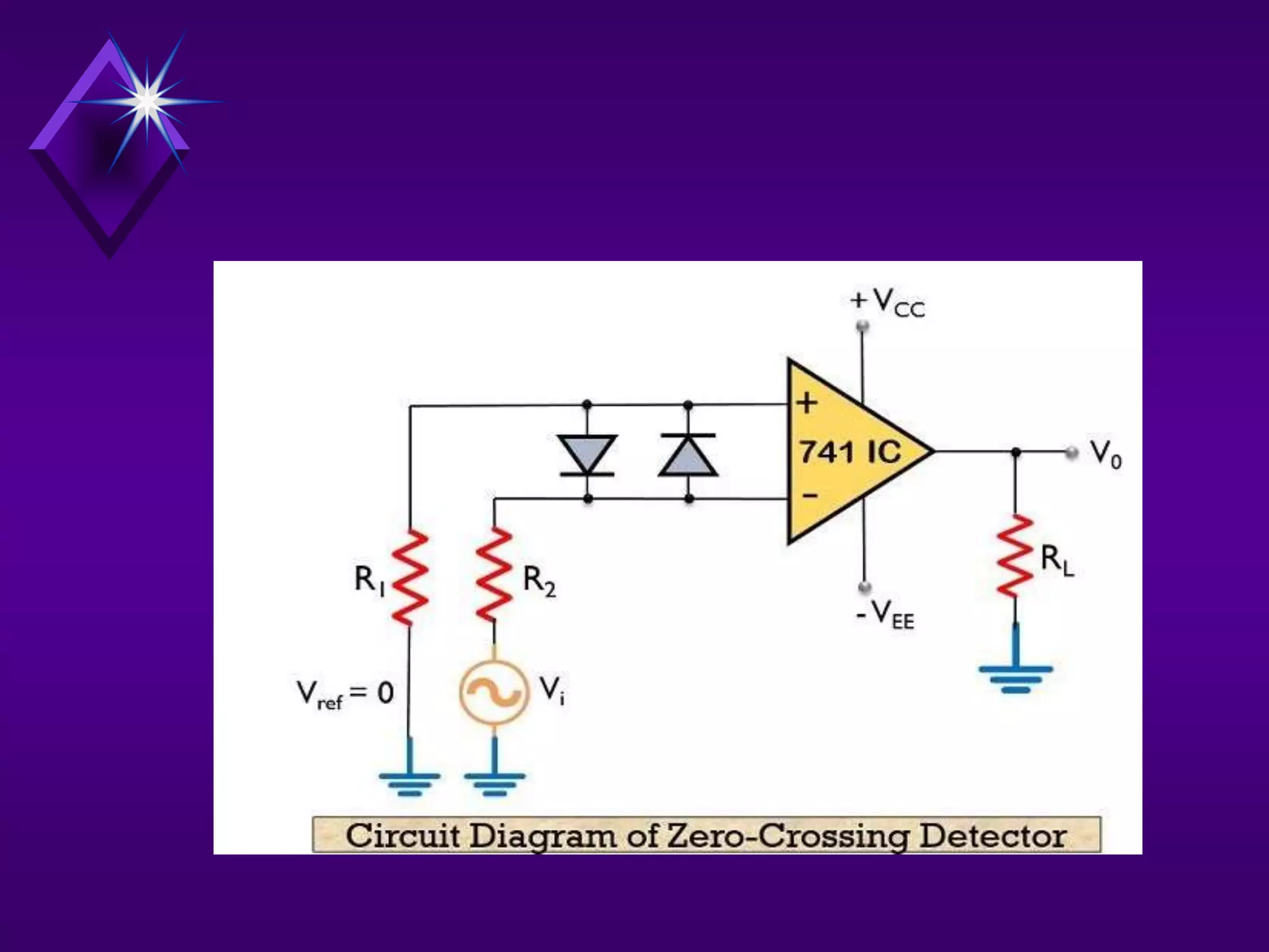
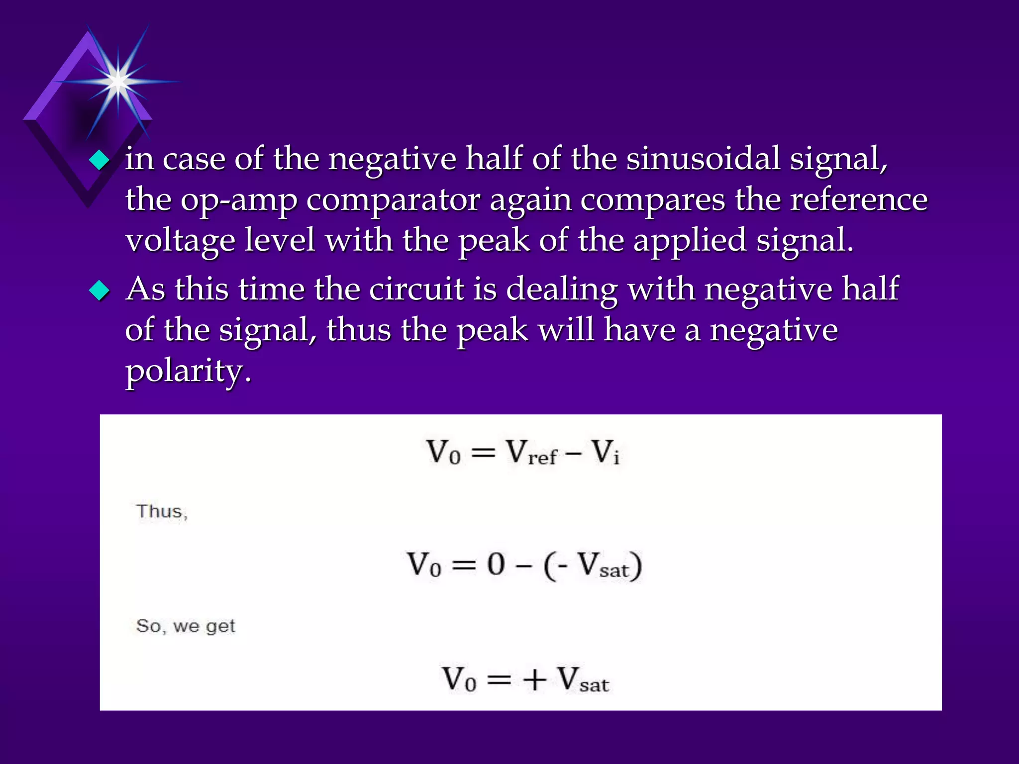
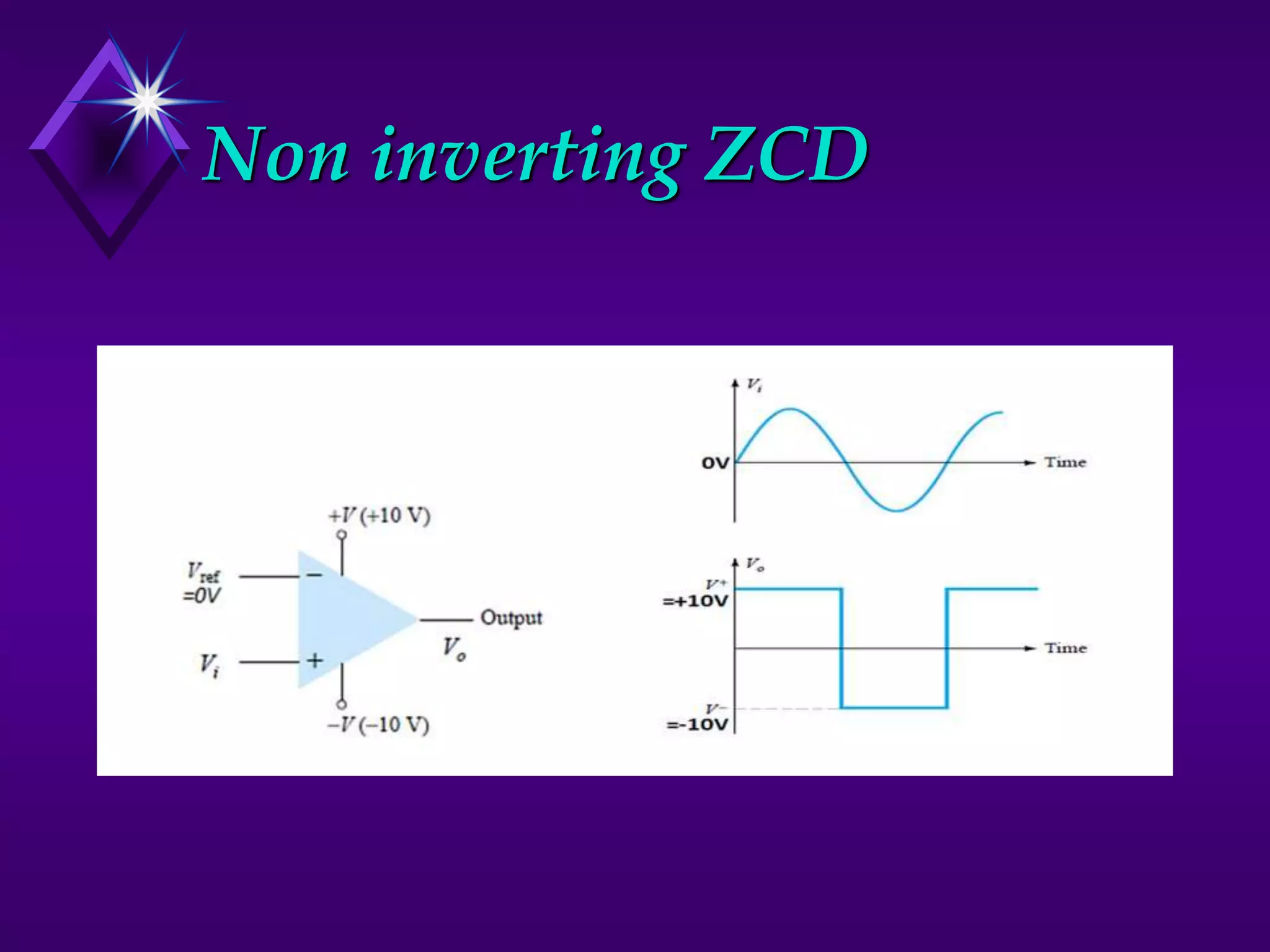
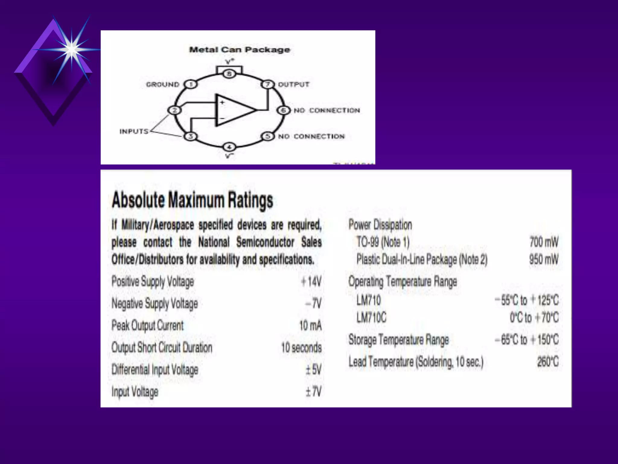
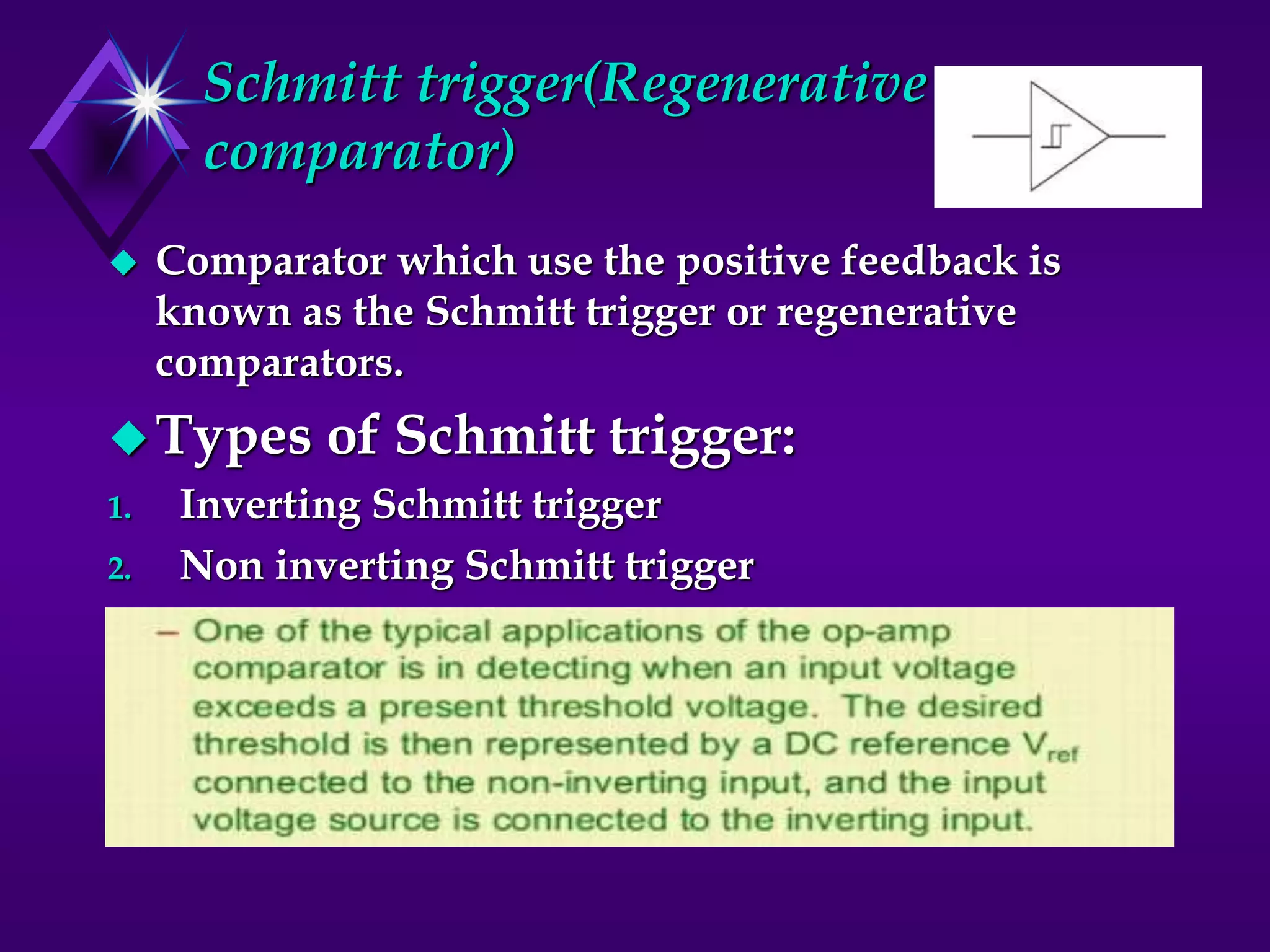
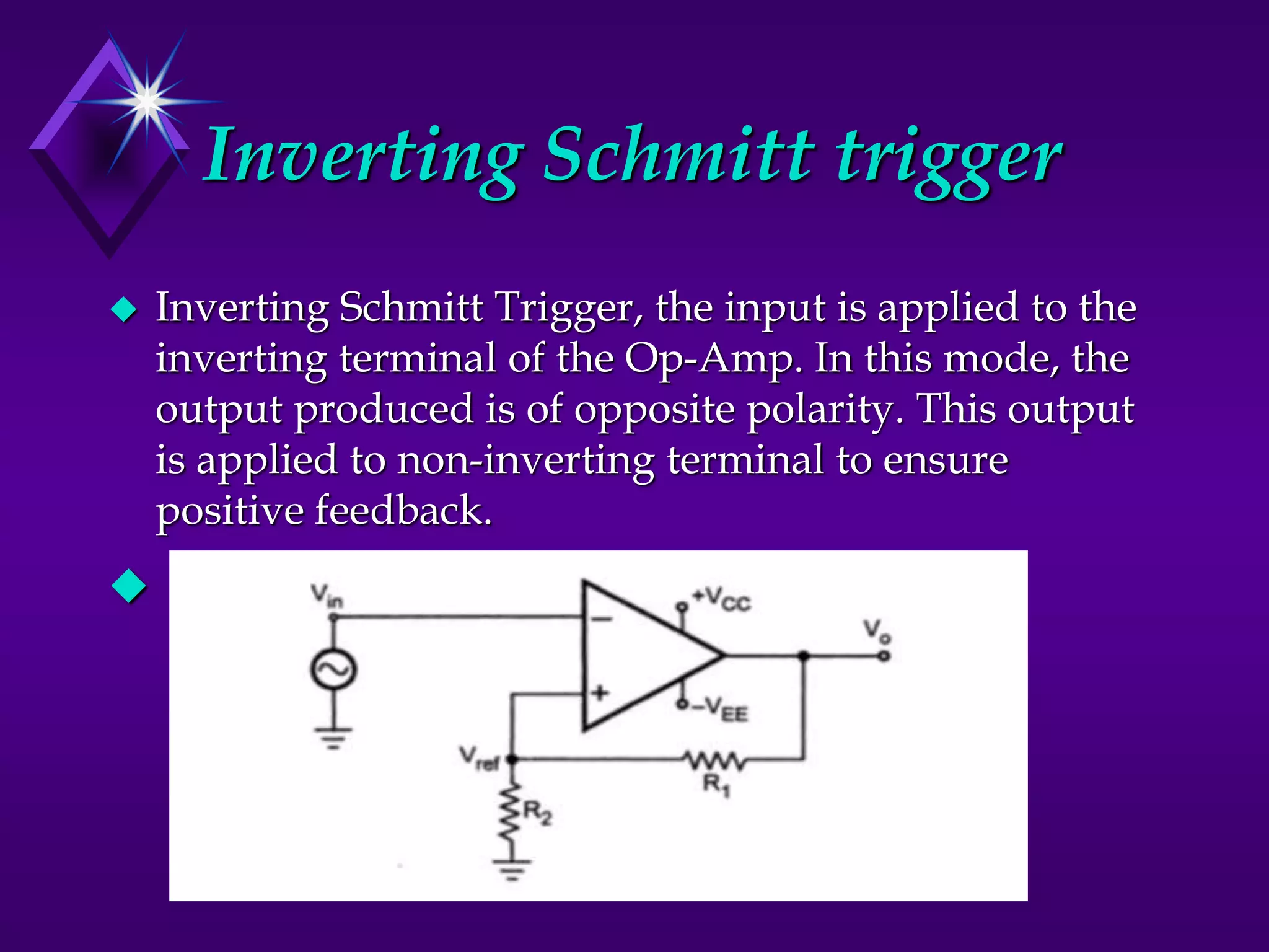
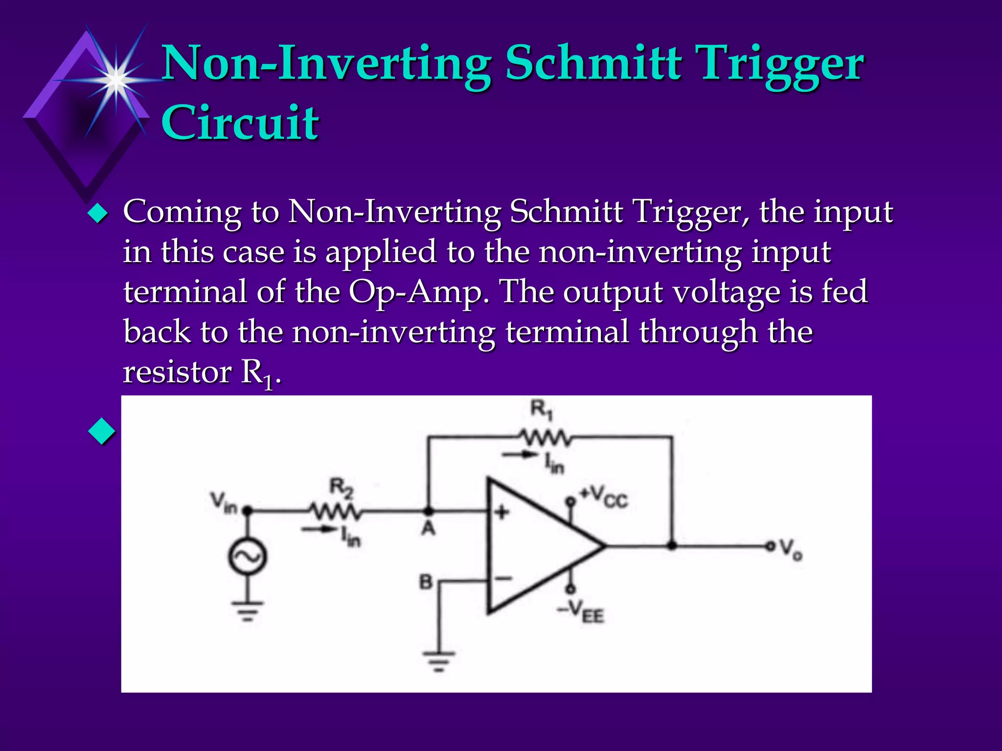
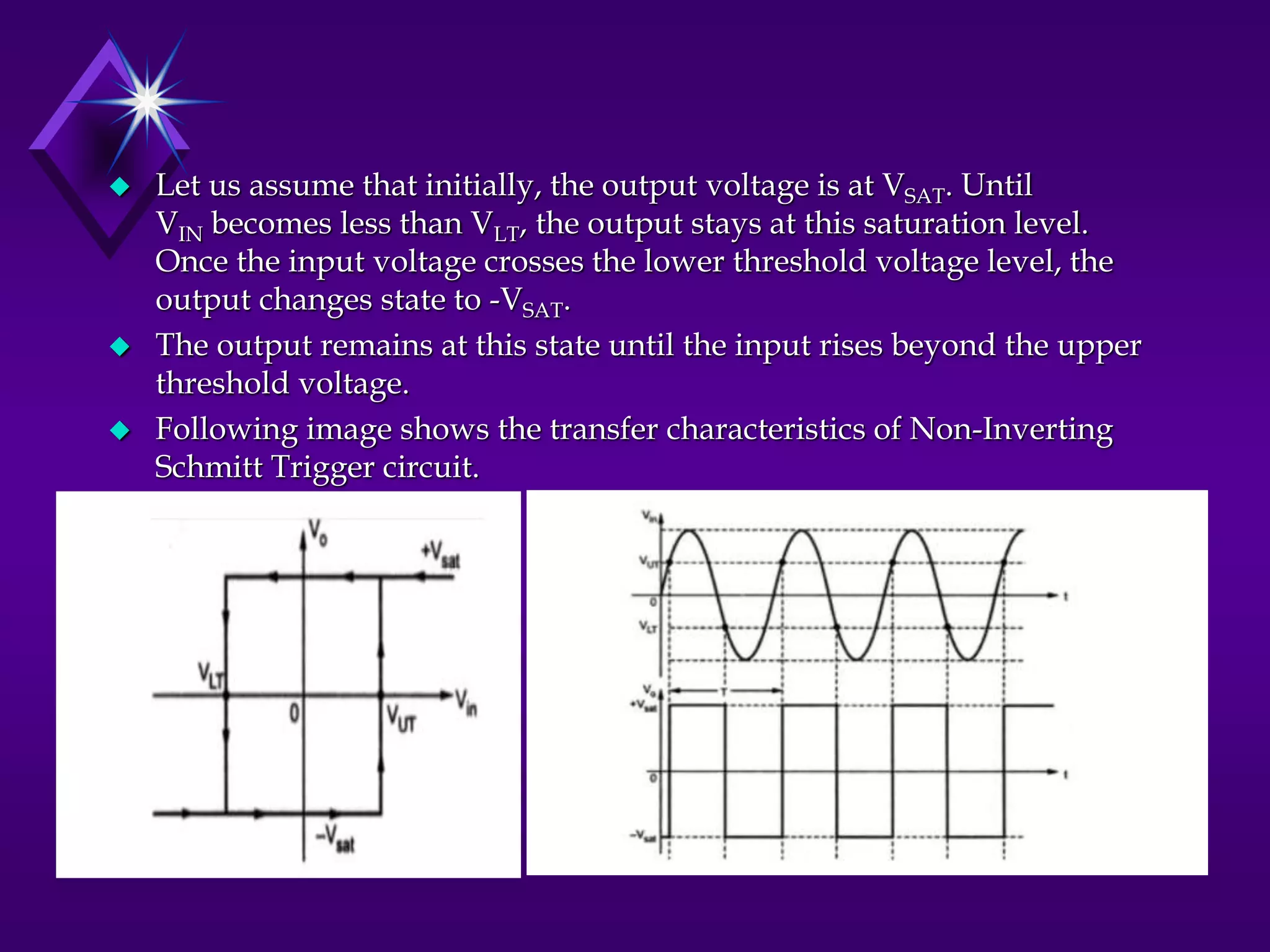
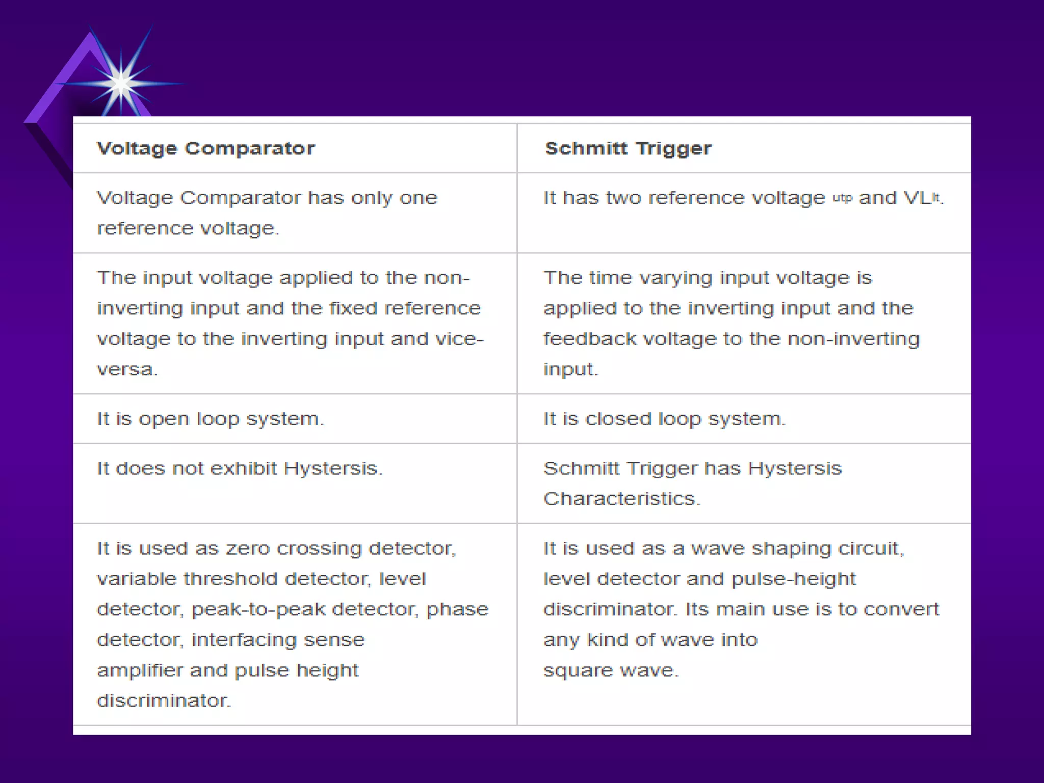
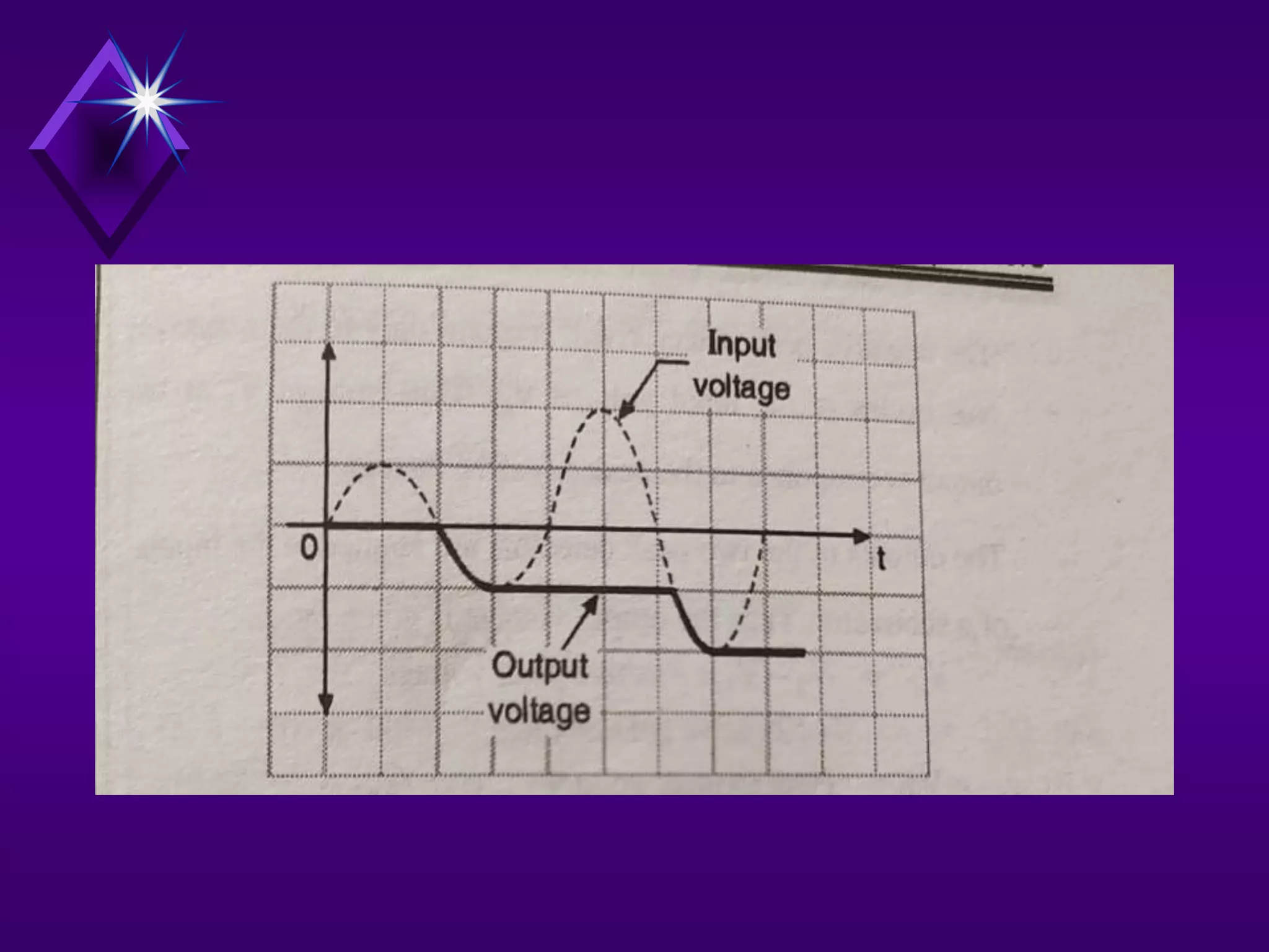
SlideShare a Scribd company logo
Comparators
S.S.Chhatwani
Introduction:
Transfer characteristics
 A comparator compares a signal voltage on one input of
an opamp with a known reference voltage on the other
input. We can say A comparator has two inputs one is
usually a constant reference voltage VR and other is a
time varying signal Vi and one output VO. We know
that in an op-amp with an open loop configuration with
a differential or single input signal has a value greater
than 0, the high gain which goes to infinity drives the
output of the op-amp into saturation. Thus, an op-amp
operating in open loop configuration will have an
output that goes to positive saturation or negative
saturation level or switch between positive and negative
saturation levels. This principle is used in a comparator
circuit with two inputs and an output.
Types of comparator
Depending on which input terminal
receives the signal input the
comparator are classified into two
categories:
Non inverting comparator
Inverting comparator
Applications:
ZCD(zero crossing detector)
Window comparator
Level detector
Phase detector
Schmitt trigger
Peak detector
Non-inverting comparator
 It is called a non-inverting comparator
circuit as the sinusoidal input signal Vin is
applied to the non-inverting terminal. The
fixed reference voltage Vref is connected to
the inverting terminal of the op-amp.
 When the value of the input voltage Vin is
greater than the reference voltage Vref the
output voltage Vo goes to positive
saturation. This is because the voltage at the
non-inverting input is greater than the
voltage at the inverting input.
 When the value of the input voltage Vin is
lesser than the reference voltage Vref, the
output voltage Vo goes to negative
saturation. This is because the voltage at the
non inverting input is smaller than the
voltage at the inverting input. Thus, output
voltage Vo changes from positive saturation
point to negative saturation point whenever
the difference between Vin and Vref
changes.
 The comparator can be called a voltage level detector,
as for a fixed value of Vref, the voltage level of Vin
can be detected. The circuit diagram shows the diodes
D1and D2.
 These two diodes are used to protect the op-amp from
damage due to increase in input voltage. These diodes
are called clamp diodes as they clamp the differential
input voltages to either 0.7V or -0.7V.
 Most op-amps do not need clamp diodes as most of
them already have built in protection.
 Resistance R1 is connected in series with input
voltage Vin and R is connected between the inverting
input and reference voltage Vref.
 R1 limits the current through the clamp diodes and R
reduces the offset problem.
Inverting amplifier
 It is called a inverting comparator circuit as
the sinusoidal input signal Vin is applied to
the inverting terminal.
 The fixed reference voltage Vref is given to
the non-inverting terminal (+) of the op-
amp. A potentiometer is used as a voltage
divider circuit to obtain the reference
voltage in the non-inverting input terminal.
 Both ends of the Potentiometer are
connected to the dc supply voltage +VCC
and -VEE. The wiper is connected to the non
inverting input terminal.
When the wiper is moved to a value near +VCC,
Vref becomes more positive, and when the wiper is
moved towards -VEE, the value of Vref becomes
more negative. The waveforms are shown below.
Inverting Comparator
 The transfer characteristics are basically a graph of output
voltage versus input voltage. From the above characteristics, it
is observed that the reference voltage (or reference point) is the
point at which the state change occurs i.e. the transition from
one state to other state. In other words, the circuit is triggered at
the reference point hence it is also called as triggering point. The
reference voltage can be changed externally and also can be
either positive or negative as discussed above. Thus the
reference point can have a trip on input axis anywhere, and
hence it is also referred as trip point or trip voltage. Also at the
reference point the state change occurs at the output when input
signal crosses the reference voltage. Thus reference voltage is
also called as threshold voltage at which the comparator is
changing its output state.
ZERO CROSSING
DETECTOR
 The zero crossing detector circuit is an
important application of the op-amp
comparator circuit. It can also be called as the
sine to square wave converter. Anyone of the
inverting or non-inverting comparators can
be used as a zero-crossing detector. The only
change to be brought in is the reference
voltage with which the input voltage is to be
compared, must be made zero (Vref = 0V).
An input sine wave is given as Vin.
 it detects the point where the input signal crosses
zero of the reference voltage level. For every crossing,
the saturation level of the output signal changes from
one to another.
 the reference level is set at 0 and applied at the non-
inverting terminal of the op-amp. The sine wave
applied at the inverting terminal of the op-amp is
compared with the reference level each time the
phase of the wave changes either from positive to
negative or negative to positive.
Firstly, when positive half of the
sinusoidal signal appears at the input.
Then the op-amp comparator compares
the reference voltage level with the
peak level of the applied signal
 in case of the negative half of the sinusoidal signal,
the op-amp comparator again compares the reference
voltage level with the peak of the applied signal.
 As this time the circuit is dealing with negative half
of the signal, thus the peak will have a negative
polarity.
 It can be seen in the above waveform that whenever
the sine wave crosses zero, the output of the Op-
amp will shift either from negative to positive or
from positive to negative.
 It shifts negative to positive when sine wave
crosses positive to negative and vice versa. This is
how a Zero Crossing Detector detects when the
waveform is crossing zero every time. As you can
observe that the output waveform is a square wave,
so a Zero Crossing Detector is also called a Square
wave Generator Circuit.
Non inverting ZCD
Limitations:
 If the input to a comparator contains noise, the output may
show error when Vin is near a trip point.
 For instance, with a zero crossing, the output is low when vin
is positive and high when vin is negative. If the input
contains a noise voltage with a peak of 1mV or more, then the
comparator will detect the zero crossing produced by the
noise. Figure below, shows the output of zero crossing
detector if the input contains noise.
Operation:

Case I:Vin<VLT & Vin<VUT
With the above two conditions, output of op-amp A1 is negative (i.e. -
Vsat) which will make the diode D1 reverse biased. Similarly output of
op-amp A2 is positive (i.e. +Vsat) which will make the diode D2
forward biased. The positive voltage, +Vsat is now applied through
potential divider formed by resistance R1 and R2 to a base of transistor
Q. Due to the positive voltage at base the npn transistor Q moves into
the saturation. Thus the output voltage is zero.
Thus upto VLT output voltage is zero.
 Case II:Vin>VLT & Vin>VUT
With the above two conditions, output of op-amp A1 is positive (i.e.
+Vsat) which will make the diode D1 forward biased. Similarly output
of op-amp A2 is negative (i.e. -Vsat) which will make the diode D2
reverse biased.
The positive voltage, +Vsat is now applied through potential divider
formed by resistance R1 and R2 to a base of transistor Q. Due to the
positive voltage at base the npn transistor Q moves into the saturation.
Thus the output voltage is zero.
Thus above VUT output voltage is zero.
 Case III:VLT<Vin<VUT
With this combined condition, both the op-amps A1
and A2 goes into negative saturation (i.e. -Vsat). Both
the diodes are reverse biased. So there is no voltage
applied for transistor Q. Thus transistor is in cut-off
and there no collector current and hence no drop
across resistance R. Thus the output voltage is
∴Vo=+5V
Thus between VLT and VUT (window of two
voltages) output voltage is high i.e. +5V and outside
this window it is zero. Therefore the circuit is called
as a window detector or comparator.
The transfer characteristic of such a window
comparator is shown below.
IC Comparators
 OPAMP IC 741 has slew rate equal to 0.5 v/µs which
is too low for its use as a comparator.
 Specially designed IC are LM311,LM339 etc.
Feature:
1. Fast switching speed due to higher slew rate
2. Output is compatible with any digital IC family
3. They have built in noise immunity .
LM 710 Voltage
comparator
 General Description:
 The LM710 series are high-speed voltage
comparators intended for use as an accurate, low-
level digital level sensor or as a replacement for
operational amplifiers in comparator applications
where speed is of prime importance. The circuit has
a differential input and a single-ended output, with
saturated output levels compatible with practically
all types of integrated logic. The device is built on a
single silicon chip which insures low offset and
thermal drift.
Features and applications
Features:
1. High accuracy
2. High speed
3. Low response time
4. Low cost
Applications:
1. Schmitt trigger
2. ADC
3. Level detector
4. Pulse width modulator
Schmitt trigger(Regenerative
comparator)
 Comparator which use the positive feedback is
known as the Schmitt trigger or regenerative
comparators.
Types of Schmitt trigger:
1. Inverting Schmitt trigger
2. Non inverting Schmitt trigger
Inverting Schmitt trigger
 Inverting Schmitt Trigger, the input is applied to the
inverting terminal of the Op-Amp. In this mode, the
output produced is of opposite polarity. This output
is applied to non-inverting terminal to ensure
positive feedback.

 When VIN is slightly greater than VREF, the output becomes -
VSAT and if VIN is slightly less that -VREF (more negative than -
VREF), then output becomes VSAT. Hence, the output voltage
VO is either at VSAT or -VSAT and the input voltage at which these
state changes occur can be controlled using R1 and R2.
 The values of VREF and -VREF can be formulated as follows:
VREF = (VO * R2) / (R1 + R2)
But VO = VSAT .
Hence,
VREF = (VSAT * R2) / (R1 + R2)
-VREF = (VO * R2) / (R1 + R2)
But VO = -VSAT . Hence,
-VREF = (-VSAT * R2) / (R1 + R2)
 The reference voltages VREF and -VREF are called
Upper Threshold Voltage VUT and Lower Threshold
Voltage VLT. The following image shows the output
voltage versus input voltage graph. It is also known
as the Transfer Characteristic of Schmitt Trigger.
Non-Inverting Schmitt Trigger
Circuit
 Coming to Non-Inverting Schmitt Trigger, the input
in this case is applied to the non-inverting input
terminal of the Op-Amp. The output voltage is fed
back to the non-inverting terminal through the
resistor R1.

 Let us assume that initially, the output voltage is at VSAT. Until
VIN becomes less than VLT, the output stays at this saturation level.
Once the input voltage crosses the lower threshold voltage level, the
output changes state to -VSAT.
 The output remains at this state until the input rises beyond the upper
threshold voltage.
 Following image shows the transfer characteristics of Non-Inverting
Schmitt Trigger circuit.
 Applications
1. One important application of Schmitt
Trigger is to convert Sine waves into Square
waves.
2. They can be used to eliminate chatter in
Comparators (a phenomenon where
multiple output transitions are produced
due to swinging of input signal through the
threshold region).
3. They can also act as simple ON / OFF
Controllers (for example, temperature based
switches).
Hysteresis
 When the input is below a different (lower) chosen
threshold the output is low, and when the input is
between the two levels the output retains its value.
This dual threshold action is called hysteresis
 Effects of hystresis:
1. It improves noise immunity
2. It reduces the response time and the operation becomes
faster.
3. It reduces the possibility of triggering produced by noise.
examples
R2=150Ω,R1=100K Ω,Vin=500mv sine
wave saturation
voltage=±15v.determine the threshold
voltages.
Peak detector using OPAMP
 Peak detector circuits are used to determine the peak
(maximum) value of an input signal. It stores the
peak value of input voltages for infinite time
duration until it comes to reset condition. Usually,
the peak of non-sinusoidal waveforms is measured
using a peak detector. As traditional ac voltmeter
cannot measure the peak of such signals.
 i) During the positive half cycle of Vin:
 the o/p of the op-amp drives D1 on. (Forward biased)
 Charging capacitor C to the positive peak value Vp of
the input volt Vin.

 ii) During the negative half cycle of Vin:
 D1 is reverse biased and voltage across C is retained.
 The only discharge path for C is through RL since the
input bias IB is negligible.
 Applications of Peak detector
 It is used in the analysis of spectral and mass
spectrometer.
 Peak detector finds its application in destructive
testing.
 It is used for instrumentation measurement, mostly
in amplitude modulated wave communication.
 It widely finds applications in sound measuring
instruments.
Negative peak detector
Peak to peak detector
Phase detector
Comparator

More Related Content

What's hot

Unit-I Characteristics of opamp
Unit-I Characteristics of opampUnit-I Characteristics of opamp
Unit-I Characteristics of opamp
Dr.Raja R
 
Integrator OP Amp
Integrator OP AmpIntegrator OP Amp
Integrator OP Amp
Dr.Raja R
 
Operational Amplifier (OpAmp)
Operational Amplifier (OpAmp)Operational Amplifier (OpAmp)
Operational Amplifier (OpAmp)
Mohammed Bamatraf
 
Instrumentation amplifier
Instrumentation amplifierInstrumentation amplifier
Instrumentation amplifier
mohdabuzar5
 
Basics of op amp
Basics of op ampBasics of op amp
Basics of op amp
Shushma Kalkura
 
Negative feedback Amplifiers
Negative feedback AmplifiersNegative feedback Amplifiers
Negative feedback Amplifiers
Yeshudas Muttu
 
Differential amplifier
Differential amplifierDifferential amplifier
Differential amplifier
sarunkutti
 
Hybrid model for Transistor, small signal Analysis
Hybrid model for Transistor, small signal AnalysisHybrid model for Transistor, small signal Analysis
Hybrid model for Transistor, small signal Analysis
Abhishek Choksi
 
Ditial to Analog Converter
Ditial to Analog ConverterDitial to Analog Converter
Ditial to Analog Converter
Gauravsinh Parmar
 
Inverting amplifier
Inverting amplifierInverting amplifier
Inverting amplifier
hepzijustin
 
Oscillators
OscillatorsOscillators
Oscillators
Neha Mannewar
 
Differential amplifier
Differential amplifierDifferential amplifier
Differential amplifier
srirenga
 
Analog to digital converters, adc
Analog to digital converters, adcAnalog to digital converters, adc
Analog to digital converters, adc
Saumya Ranjan Behura
 
Schmitt trigger circuit
Schmitt trigger circuitSchmitt trigger circuit
Schmitt trigger circuit
taranjeet10
 
Operational amplifier
Operational amplifierOperational amplifier
Operational amplifier
Muhd Iqwan Mustaffa
 
Phase locked loop
Phase locked loopPhase locked loop
Phase locked loop
Preet_patel
 
Dual Slope ADC.pptx
Dual Slope ADC.pptxDual Slope ADC.pptx
Dual Slope ADC.pptx
hepzijustin
 
Comparator, Zero Crossing Detector and schmitt trigger using opamp
Comparator, Zero Crossing Detector and schmitt trigger using opampComparator, Zero Crossing Detector and schmitt trigger using opamp
Comparator, Zero Crossing Detector and schmitt trigger using opamp
Divyanshu Rai
 
3.bipolar junction transistor (bjt)
3.bipolar junction transistor (bjt)3.bipolar junction transistor (bjt)
3.bipolar junction transistor (bjt)
firozamin
 
Presentation on Op-amp by Sourabh kumar
Presentation on Op-amp by Sourabh kumarPresentation on Op-amp by Sourabh kumar
Presentation on Op-amp by Sourabh kumar
Sourabh Kumar
 

What's hot (20)

Unit-I Characteristics of opamp
Unit-I Characteristics of opampUnit-I Characteristics of opamp
Unit-I Characteristics of opamp
 
Integrator OP Amp
Integrator OP AmpIntegrator OP Amp
Integrator OP Amp
 
Operational Amplifier (OpAmp)
Operational Amplifier (OpAmp)Operational Amplifier (OpAmp)
Operational Amplifier (OpAmp)
 
Instrumentation amplifier
Instrumentation amplifierInstrumentation amplifier
Instrumentation amplifier
 
Basics of op amp
Basics of op ampBasics of op amp
Basics of op amp
 
Negative feedback Amplifiers
Negative feedback AmplifiersNegative feedback Amplifiers
Negative feedback Amplifiers
 
Differential amplifier
Differential amplifierDifferential amplifier
Differential amplifier
 
Hybrid model for Transistor, small signal Analysis
Hybrid model for Transistor, small signal AnalysisHybrid model for Transistor, small signal Analysis
Hybrid model for Transistor, small signal Analysis
 
Ditial to Analog Converter
Ditial to Analog ConverterDitial to Analog Converter
Ditial to Analog Converter
 
Inverting amplifier
Inverting amplifierInverting amplifier
Inverting amplifier
 
Oscillators
OscillatorsOscillators
Oscillators
 
Differential amplifier
Differential amplifierDifferential amplifier
Differential amplifier
 
Analog to digital converters, adc
Analog to digital converters, adcAnalog to digital converters, adc
Analog to digital converters, adc
 
Schmitt trigger circuit
Schmitt trigger circuitSchmitt trigger circuit
Schmitt trigger circuit
 
Operational amplifier
Operational amplifierOperational amplifier
Operational amplifier
 
Phase locked loop
Phase locked loopPhase locked loop
Phase locked loop
 
Dual Slope ADC.pptx
Dual Slope ADC.pptxDual Slope ADC.pptx
Dual Slope ADC.pptx
 
Comparator, Zero Crossing Detector and schmitt trigger using opamp
Comparator, Zero Crossing Detector and schmitt trigger using opampComparator, Zero Crossing Detector and schmitt trigger using opamp
Comparator, Zero Crossing Detector and schmitt trigger using opamp
 
3.bipolar junction transistor (bjt)
3.bipolar junction transistor (bjt)3.bipolar junction transistor (bjt)
3.bipolar junction transistor (bjt)
 
Presentation on Op-amp by Sourabh kumar
Presentation on Op-amp by Sourabh kumarPresentation on Op-amp by Sourabh kumar
Presentation on Op-amp by Sourabh kumar
 

Similar to Comparator

04.ppt
04.ppt04.ppt
Non linear applications of op amp
Non linear applications of op amp Non linear applications of op amp
Non linear applications of op amp
AsheeshKumar67
 
linear5 circuit analysis Charateristics of Op-Amp.ppt
linear5 circuit analysis Charateristics of Op-Amp.pptlinear5 circuit analysis Charateristics of Op-Amp.ppt
linear5 circuit analysis Charateristics of Op-Amp.ppt
daminiuvarani
 
zero cross detector.pptx
zero cross detector.pptxzero cross detector.pptx
zero cross detector.pptx
Aman bharti
 
analog elecronic designLecture 2 (1).pptx
analog elecronic designLecture 2 (1).pptxanalog elecronic designLecture 2 (1).pptx
analog elecronic designLecture 2 (1).pptx
YonaCastro1
 
UNIT-3 OPAMP.pptx
UNIT-3 OPAMP.pptxUNIT-3 OPAMP.pptx
UNIT-3 OPAMP.pptx
yogitapatil87
 
Operation amplifier
Operation amplifierOperation amplifier
Operation amplifier
Djukarna Djapri
 
Operationamplifier
OperationamplifierOperationamplifier
Operationamplifier
Ahmad Al-Jmal
 
Chapter 7: Operational Amplifier (Op-Amp)
Chapter 7: Operational Amplifier (Op-Amp)Chapter 7: Operational Amplifier (Op-Amp)
Chapter 7: Operational Amplifier (Op-Amp)
JeremyLauKarHei
 
1&2.pptx
1&2.pptx1&2.pptx
1&2.pptx
ragu nath
 
Unit-6 ae 3rd sem by Prof Priyanka Jain.pptx
Unit-6 ae 3rd sem by Prof Priyanka Jain.pptxUnit-6 ae 3rd sem by Prof Priyanka Jain.pptx
Unit-6 ae 3rd sem by Prof Priyanka Jain.pptx
amitthory13012003
 
Basic Electronics 5 by Dr. Mathivanan Velumani
Basic Electronics 5 by Dr. Mathivanan VelumaniBasic Electronics 5 by Dr. Mathivanan Velumani
Basic Electronics 5 by Dr. Mathivanan Velumani
Mathivanan Velumani
 
Operational Amplifiers
Operational AmplifiersOperational Amplifiers
Operational Amplifiers
Mahesh_Naidu
 
Agdon
AgdonAgdon
opamp
opampopamp
Electrical signal processing and transmission
Electrical signal processing and transmissionElectrical signal processing and transmission
Electrical signal processing and transmission
Bishal Rimal
 
Op-Amp 1
Op-Amp 1Op-Amp 1
ppt ac.pptx
ppt ac.pptxppt ac.pptx
ppt ac.pptx
BitEte
 
Peakdetector
PeakdetectorPeakdetector
Peakdetector
Manjunath Achari
 
Operating Amplifier
Operating AmplifierOperating Amplifier
Operating Amplifier
BalajiK109
 

Similar to Comparator (20)

04.ppt
04.ppt04.ppt
04.ppt
 
Non linear applications of op amp
Non linear applications of op amp Non linear applications of op amp
Non linear applications of op amp
 
linear5 circuit analysis Charateristics of Op-Amp.ppt
linear5 circuit analysis Charateristics of Op-Amp.pptlinear5 circuit analysis Charateristics of Op-Amp.ppt
linear5 circuit analysis Charateristics of Op-Amp.ppt
 
zero cross detector.pptx
zero cross detector.pptxzero cross detector.pptx
zero cross detector.pptx
 
analog elecronic designLecture 2 (1).pptx
analog elecronic designLecture 2 (1).pptxanalog elecronic designLecture 2 (1).pptx
analog elecronic designLecture 2 (1).pptx
 
UNIT-3 OPAMP.pptx
UNIT-3 OPAMP.pptxUNIT-3 OPAMP.pptx
UNIT-3 OPAMP.pptx
 
Operation amplifier
Operation amplifierOperation amplifier
Operation amplifier
 
Operationamplifier
OperationamplifierOperationamplifier
Operationamplifier
 
Chapter 7: Operational Amplifier (Op-Amp)
Chapter 7: Operational Amplifier (Op-Amp)Chapter 7: Operational Amplifier (Op-Amp)
Chapter 7: Operational Amplifier (Op-Amp)
 
1&2.pptx
1&2.pptx1&2.pptx
1&2.pptx
 
Unit-6 ae 3rd sem by Prof Priyanka Jain.pptx
Unit-6 ae 3rd sem by Prof Priyanka Jain.pptxUnit-6 ae 3rd sem by Prof Priyanka Jain.pptx
Unit-6 ae 3rd sem by Prof Priyanka Jain.pptx
 
Basic Electronics 5 by Dr. Mathivanan Velumani
Basic Electronics 5 by Dr. Mathivanan VelumaniBasic Electronics 5 by Dr. Mathivanan Velumani
Basic Electronics 5 by Dr. Mathivanan Velumani
 
Operational Amplifiers
Operational AmplifiersOperational Amplifiers
Operational Amplifiers
 
Agdon
AgdonAgdon
Agdon
 
opamp
opampopamp
opamp
 
Electrical signal processing and transmission
Electrical signal processing and transmissionElectrical signal processing and transmission
Electrical signal processing and transmission
 
Op-Amp 1
Op-Amp 1Op-Amp 1
Op-Amp 1
 
ppt ac.pptx
ppt ac.pptxppt ac.pptx
ppt ac.pptx
 
Peakdetector
PeakdetectorPeakdetector
Peakdetector
 
Operating Amplifier
Operating AmplifierOperating Amplifier
Operating Amplifier
 

Recently uploaded

Exception Handling notes in java exception
Exception Handling notes in java exceptionException Handling notes in java exception
Exception Handling notes in java exception
Ratnakar Mikkili
 
14 Template Contractual Notice - EOT Application
14 Template Contractual Notice - EOT Application14 Template Contractual Notice - EOT Application
14 Template Contractual Notice - EOT Application
SyedAbiiAzazi1
 
Generative AI leverages algorithms to create various forms of content
Generative AI leverages algorithms to create various forms of contentGenerative AI leverages algorithms to create various forms of content
Generative AI leverages algorithms to create various forms of content
Hitesh Mohapatra
 
Presentation of IEEE Slovenia CIS (Computational Intelligence Society) Chapte...
Presentation of IEEE Slovenia CIS (Computational Intelligence Society) Chapte...Presentation of IEEE Slovenia CIS (Computational Intelligence Society) Chapte...
Presentation of IEEE Slovenia CIS (Computational Intelligence Society) Chapte...
University of Maribor
 
5214-1693458878915-Unit 6 2023 to 2024 academic year assignment (AutoRecovere...
5214-1693458878915-Unit 6 2023 to 2024 academic year assignment (AutoRecovere...5214-1693458878915-Unit 6 2023 to 2024 academic year assignment (AutoRecovere...
5214-1693458878915-Unit 6 2023 to 2024 academic year assignment (AutoRecovere...
ihlasbinance2003
 
Wearable antenna for antenna applications
Wearable antenna for antenna applicationsWearable antenna for antenna applications
Wearable antenna for antenna applications
Madhumitha Jayaram
 
ACRP 4-09 Risk Assessment Method to Support Modification of Airfield Separat...
ACRP 4-09 Risk Assessment Method to Support Modification of Airfield Separat...ACRP 4-09 Risk Assessment Method to Support Modification of Airfield Separat...
ACRP 4-09 Risk Assessment Method to Support Modification of Airfield Separat...
Mukeshwaran Balu
 
Swimming pool mechanical components design.pptx
Swimming pool  mechanical components design.pptxSwimming pool  mechanical components design.pptx
Swimming pool mechanical components design.pptx
yokeleetan1
 
Low power architecture of logic gates using adiabatic techniques
Low power architecture of logic gates using adiabatic techniquesLow power architecture of logic gates using adiabatic techniques
Low power architecture of logic gates using adiabatic techniques
nooriasukmaningtyas
 
22CYT12-Unit-V-E Waste and its Management.ppt
22CYT12-Unit-V-E Waste and its Management.ppt22CYT12-Unit-V-E Waste and its Management.ppt
22CYT12-Unit-V-E Waste and its Management.ppt
KrishnaveniKrishnara1
 
Harnessing WebAssembly for Real-time Stateless Streaming Pipelines
Harnessing WebAssembly for Real-time Stateless Streaming PipelinesHarnessing WebAssembly for Real-time Stateless Streaming Pipelines
Harnessing WebAssembly for Real-time Stateless Streaming Pipelines
Christina Lin
 
Properties Railway Sleepers and Test.pptx
Properties Railway Sleepers and Test.pptxProperties Railway Sleepers and Test.pptx
Properties Railway Sleepers and Test.pptx
MDSABBIROJJAMANPAYEL
 
KuberTENes Birthday Bash Guadalajara - K8sGPT first impressions
KuberTENes Birthday Bash Guadalajara - K8sGPT first impressionsKuberTENes Birthday Bash Guadalajara - K8sGPT first impressions
KuberTENes Birthday Bash Guadalajara - K8sGPT first impressions
Victor Morales
 
Manufacturing Process of molasses based distillery ppt.pptx
Manufacturing Process of molasses based distillery ppt.pptxManufacturing Process of molasses based distillery ppt.pptx
Manufacturing Process of molasses based distillery ppt.pptx
Madan Karki
 
Recycled Concrete Aggregate in Construction Part III
Recycled Concrete Aggregate in Construction Part IIIRecycled Concrete Aggregate in Construction Part III
Recycled Concrete Aggregate in Construction Part III
Aditya Rajan Patra
 
Heat Resistant Concrete Presentation ppt
Heat Resistant Concrete Presentation pptHeat Resistant Concrete Presentation ppt
Heat Resistant Concrete Presentation ppt
mamunhossenbd75
 
sieving analysis and results interpretation
sieving analysis and results interpretationsieving analysis and results interpretation
sieving analysis and results interpretation
ssuser36d3051
 
Electric vehicle and photovoltaic advanced roles in enhancing the financial p...
Electric vehicle and photovoltaic advanced roles in enhancing the financial p...Electric vehicle and photovoltaic advanced roles in enhancing the financial p...
Electric vehicle and photovoltaic advanced roles in enhancing the financial p...
IJECEIAES
 
IEEE Aerospace and Electronic Systems Society as a Graduate Student Member
IEEE Aerospace and Electronic Systems Society as a Graduate Student MemberIEEE Aerospace and Electronic Systems Society as a Graduate Student Member
IEEE Aerospace and Electronic Systems Society as a Graduate Student Member
VICTOR MAESTRE RAMIREZ
 
Technical Drawings introduction to drawing of prisms
Technical Drawings introduction to drawing of prismsTechnical Drawings introduction to drawing of prisms
Technical Drawings introduction to drawing of prisms
heavyhaig
 

Recently uploaded (20)

Exception Handling notes in java exception
Exception Handling notes in java exceptionException Handling notes in java exception
Exception Handling notes in java exception
 
14 Template Contractual Notice - EOT Application
14 Template Contractual Notice - EOT Application14 Template Contractual Notice - EOT Application
14 Template Contractual Notice - EOT Application
 
Generative AI leverages algorithms to create various forms of content
Generative AI leverages algorithms to create various forms of contentGenerative AI leverages algorithms to create various forms of content
Generative AI leverages algorithms to create various forms of content
 
Presentation of IEEE Slovenia CIS (Computational Intelligence Society) Chapte...
Presentation of IEEE Slovenia CIS (Computational Intelligence Society) Chapte...Presentation of IEEE Slovenia CIS (Computational Intelligence Society) Chapte...
Presentation of IEEE Slovenia CIS (Computational Intelligence Society) Chapte...
 
5214-1693458878915-Unit 6 2023 to 2024 academic year assignment (AutoRecovere...
5214-1693458878915-Unit 6 2023 to 2024 academic year assignment (AutoRecovere...5214-1693458878915-Unit 6 2023 to 2024 academic year assignment (AutoRecovere...
5214-1693458878915-Unit 6 2023 to 2024 academic year assignment (AutoRecovere...
 
Wearable antenna for antenna applications
Wearable antenna for antenna applicationsWearable antenna for antenna applications
Wearable antenna for antenna applications
 
ACRP 4-09 Risk Assessment Method to Support Modification of Airfield Separat...
ACRP 4-09 Risk Assessment Method to Support Modification of Airfield Separat...ACRP 4-09 Risk Assessment Method to Support Modification of Airfield Separat...
ACRP 4-09 Risk Assessment Method to Support Modification of Airfield Separat...
 
Swimming pool mechanical components design.pptx
Swimming pool  mechanical components design.pptxSwimming pool  mechanical components design.pptx
Swimming pool mechanical components design.pptx
 
Low power architecture of logic gates using adiabatic techniques
Low power architecture of logic gates using adiabatic techniquesLow power architecture of logic gates using adiabatic techniques
Low power architecture of logic gates using adiabatic techniques
 
22CYT12-Unit-V-E Waste and its Management.ppt
22CYT12-Unit-V-E Waste and its Management.ppt22CYT12-Unit-V-E Waste and its Management.ppt
22CYT12-Unit-V-E Waste and its Management.ppt
 
Harnessing WebAssembly for Real-time Stateless Streaming Pipelines
Harnessing WebAssembly for Real-time Stateless Streaming PipelinesHarnessing WebAssembly for Real-time Stateless Streaming Pipelines
Harnessing WebAssembly for Real-time Stateless Streaming Pipelines
 
Properties Railway Sleepers and Test.pptx
Properties Railway Sleepers and Test.pptxProperties Railway Sleepers and Test.pptx
Properties Railway Sleepers and Test.pptx
 
KuberTENes Birthday Bash Guadalajara - K8sGPT first impressions
KuberTENes Birthday Bash Guadalajara - K8sGPT first impressionsKuberTENes Birthday Bash Guadalajara - K8sGPT first impressions
KuberTENes Birthday Bash Guadalajara - K8sGPT first impressions
 
Manufacturing Process of molasses based distillery ppt.pptx
Manufacturing Process of molasses based distillery ppt.pptxManufacturing Process of molasses based distillery ppt.pptx
Manufacturing Process of molasses based distillery ppt.pptx
 
Recycled Concrete Aggregate in Construction Part III
Recycled Concrete Aggregate in Construction Part IIIRecycled Concrete Aggregate in Construction Part III
Recycled Concrete Aggregate in Construction Part III
 
Heat Resistant Concrete Presentation ppt
Heat Resistant Concrete Presentation pptHeat Resistant Concrete Presentation ppt
Heat Resistant Concrete Presentation ppt
 
sieving analysis and results interpretation
sieving analysis and results interpretationsieving analysis and results interpretation
sieving analysis and results interpretation
 
Electric vehicle and photovoltaic advanced roles in enhancing the financial p...
Electric vehicle and photovoltaic advanced roles in enhancing the financial p...Electric vehicle and photovoltaic advanced roles in enhancing the financial p...
Electric vehicle and photovoltaic advanced roles in enhancing the financial p...
 
IEEE Aerospace and Electronic Systems Society as a Graduate Student Member
IEEE Aerospace and Electronic Systems Society as a Graduate Student MemberIEEE Aerospace and Electronic Systems Society as a Graduate Student Member
IEEE Aerospace and Electronic Systems Society as a Graduate Student Member
 
Technical Drawings introduction to drawing of prisms
Technical Drawings introduction to drawing of prismsTechnical Drawings introduction to drawing of prisms
Technical Drawings introduction to drawing of prisms
 

Comparator

  • 3.
  • 4.
  • 5.
  • 7.
  • 8.  A comparator compares a signal voltage on one input of an opamp with a known reference voltage on the other input. We can say A comparator has two inputs one is usually a constant reference voltage VR and other is a time varying signal Vi and one output VO. We know that in an op-amp with an open loop configuration with a differential or single input signal has a value greater than 0, the high gain which goes to infinity drives the output of the op-amp into saturation. Thus, an op-amp operating in open loop configuration will have an output that goes to positive saturation or negative saturation level or switch between positive and negative saturation levels. This principle is used in a comparator circuit with two inputs and an output.
  • 9.
  • 10. Types of comparator Depending on which input terminal receives the signal input the comparator are classified into two categories: Non inverting comparator Inverting comparator
  • 11. Applications: ZCD(zero crossing detector) Window comparator Level detector Phase detector Schmitt trigger Peak detector
  • 13.  It is called a non-inverting comparator circuit as the sinusoidal input signal Vin is applied to the non-inverting terminal. The fixed reference voltage Vref is connected to the inverting terminal of the op-amp.  When the value of the input voltage Vin is greater than the reference voltage Vref the output voltage Vo goes to positive saturation. This is because the voltage at the non-inverting input is greater than the voltage at the inverting input.
  • 14.  When the value of the input voltage Vin is lesser than the reference voltage Vref, the output voltage Vo goes to negative saturation. This is because the voltage at the non inverting input is smaller than the voltage at the inverting input. Thus, output voltage Vo changes from positive saturation point to negative saturation point whenever the difference between Vin and Vref changes.
  • 15.  The comparator can be called a voltage level detector, as for a fixed value of Vref, the voltage level of Vin can be detected. The circuit diagram shows the diodes D1and D2.  These two diodes are used to protect the op-amp from damage due to increase in input voltage. These diodes are called clamp diodes as they clamp the differential input voltages to either 0.7V or -0.7V.  Most op-amps do not need clamp diodes as most of them already have built in protection.  Resistance R1 is connected in series with input voltage Vin and R is connected between the inverting input and reference voltage Vref.  R1 limits the current through the clamp diodes and R reduces the offset problem.
  • 16.
  • 18.  It is called a inverting comparator circuit as the sinusoidal input signal Vin is applied to the inverting terminal.  The fixed reference voltage Vref is given to the non-inverting terminal (+) of the op- amp. A potentiometer is used as a voltage divider circuit to obtain the reference voltage in the non-inverting input terminal.  Both ends of the Potentiometer are connected to the dc supply voltage +VCC and -VEE. The wiper is connected to the non inverting input terminal.
  • 19. When the wiper is moved to a value near +VCC, Vref becomes more positive, and when the wiper is moved towards -VEE, the value of Vref becomes more negative. The waveforms are shown below.
  • 21.  The transfer characteristics are basically a graph of output voltage versus input voltage. From the above characteristics, it is observed that the reference voltage (or reference point) is the point at which the state change occurs i.e. the transition from one state to other state. In other words, the circuit is triggered at the reference point hence it is also called as triggering point. The reference voltage can be changed externally and also can be either positive or negative as discussed above. Thus the reference point can have a trip on input axis anywhere, and hence it is also referred as trip point or trip voltage. Also at the reference point the state change occurs at the output when input signal crosses the reference voltage. Thus reference voltage is also called as threshold voltage at which the comparator is changing its output state.
  • 22.
  • 23. ZERO CROSSING DETECTOR  The zero crossing detector circuit is an important application of the op-amp comparator circuit. It can also be called as the sine to square wave converter. Anyone of the inverting or non-inverting comparators can be used as a zero-crossing detector. The only change to be brought in is the reference voltage with which the input voltage is to be compared, must be made zero (Vref = 0V). An input sine wave is given as Vin.
  • 24.
  • 25.
  • 26.  it detects the point where the input signal crosses zero of the reference voltage level. For every crossing, the saturation level of the output signal changes from one to another.  the reference level is set at 0 and applied at the non- inverting terminal of the op-amp. The sine wave applied at the inverting terminal of the op-amp is compared with the reference level each time the phase of the wave changes either from positive to negative or negative to positive.
  • 27. Firstly, when positive half of the sinusoidal signal appears at the input. Then the op-amp comparator compares the reference voltage level with the peak level of the applied signal
  • 28.  in case of the negative half of the sinusoidal signal, the op-amp comparator again compares the reference voltage level with the peak of the applied signal.  As this time the circuit is dealing with negative half of the signal, thus the peak will have a negative polarity.
  • 29.  It can be seen in the above waveform that whenever the sine wave crosses zero, the output of the Op- amp will shift either from negative to positive or from positive to negative.  It shifts negative to positive when sine wave crosses positive to negative and vice versa. This is how a Zero Crossing Detector detects when the waveform is crossing zero every time. As you can observe that the output waveform is a square wave, so a Zero Crossing Detector is also called a Square wave Generator Circuit.
  • 31. Limitations:  If the input to a comparator contains noise, the output may show error when Vin is near a trip point.  For instance, with a zero crossing, the output is low when vin is positive and high when vin is negative. If the input contains a noise voltage with a peak of 1mV or more, then the comparator will detect the zero crossing produced by the noise. Figure below, shows the output of zero crossing detector if the input contains noise.
  • 32.
  • 33.
  • 34. Operation:  Case I:Vin<VLT & Vin<VUT With the above two conditions, output of op-amp A1 is negative (i.e. - Vsat) which will make the diode D1 reverse biased. Similarly output of op-amp A2 is positive (i.e. +Vsat) which will make the diode D2 forward biased. The positive voltage, +Vsat is now applied through potential divider formed by resistance R1 and R2 to a base of transistor Q. Due to the positive voltage at base the npn transistor Q moves into the saturation. Thus the output voltage is zero. Thus upto VLT output voltage is zero.  Case II:Vin>VLT & Vin>VUT With the above two conditions, output of op-amp A1 is positive (i.e. +Vsat) which will make the diode D1 forward biased. Similarly output of op-amp A2 is negative (i.e. -Vsat) which will make the diode D2 reverse biased. The positive voltage, +Vsat is now applied through potential divider formed by resistance R1 and R2 to a base of transistor Q. Due to the positive voltage at base the npn transistor Q moves into the saturation. Thus the output voltage is zero. Thus above VUT output voltage is zero.
  • 35.  Case III:VLT<Vin<VUT With this combined condition, both the op-amps A1 and A2 goes into negative saturation (i.e. -Vsat). Both the diodes are reverse biased. So there is no voltage applied for transistor Q. Thus transistor is in cut-off and there no collector current and hence no drop across resistance R. Thus the output voltage is ∴Vo=+5V Thus between VLT and VUT (window of two voltages) output voltage is high i.e. +5V and outside this window it is zero. Therefore the circuit is called as a window detector or comparator. The transfer characteristic of such a window comparator is shown below.
  • 36.
  • 37. IC Comparators  OPAMP IC 741 has slew rate equal to 0.5 v/µs which is too low for its use as a comparator.  Specially designed IC are LM311,LM339 etc. Feature: 1. Fast switching speed due to higher slew rate 2. Output is compatible with any digital IC family 3. They have built in noise immunity .
  • 38. LM 710 Voltage comparator  General Description:  The LM710 series are high-speed voltage comparators intended for use as an accurate, low- level digital level sensor or as a replacement for operational amplifiers in comparator applications where speed is of prime importance. The circuit has a differential input and a single-ended output, with saturated output levels compatible with practically all types of integrated logic. The device is built on a single silicon chip which insures low offset and thermal drift.
  • 39.
  • 40. Features and applications Features: 1. High accuracy 2. High speed 3. Low response time 4. Low cost Applications: 1. Schmitt trigger 2. ADC 3. Level detector 4. Pulse width modulator
  • 41. Schmitt trigger(Regenerative comparator)  Comparator which use the positive feedback is known as the Schmitt trigger or regenerative comparators. Types of Schmitt trigger: 1. Inverting Schmitt trigger 2. Non inverting Schmitt trigger
  • 42. Inverting Schmitt trigger  Inverting Schmitt Trigger, the input is applied to the inverting terminal of the Op-Amp. In this mode, the output produced is of opposite polarity. This output is applied to non-inverting terminal to ensure positive feedback. 
  • 43.  When VIN is slightly greater than VREF, the output becomes - VSAT and if VIN is slightly less that -VREF (more negative than - VREF), then output becomes VSAT. Hence, the output voltage VO is either at VSAT or -VSAT and the input voltage at which these state changes occur can be controlled using R1 and R2.  The values of VREF and -VREF can be formulated as follows: VREF = (VO * R2) / (R1 + R2) But VO = VSAT . Hence, VREF = (VSAT * R2) / (R1 + R2) -VREF = (VO * R2) / (R1 + R2) But VO = -VSAT . Hence, -VREF = (-VSAT * R2) / (R1 + R2)
  • 44.  The reference voltages VREF and -VREF are called Upper Threshold Voltage VUT and Lower Threshold Voltage VLT. The following image shows the output voltage versus input voltage graph. It is also known as the Transfer Characteristic of Schmitt Trigger.
  • 45. Non-Inverting Schmitt Trigger Circuit  Coming to Non-Inverting Schmitt Trigger, the input in this case is applied to the non-inverting input terminal of the Op-Amp. The output voltage is fed back to the non-inverting terminal through the resistor R1. 
  • 46.  Let us assume that initially, the output voltage is at VSAT. Until VIN becomes less than VLT, the output stays at this saturation level. Once the input voltage crosses the lower threshold voltage level, the output changes state to -VSAT.  The output remains at this state until the input rises beyond the upper threshold voltage.  Following image shows the transfer characteristics of Non-Inverting Schmitt Trigger circuit.
  • 47.  Applications 1. One important application of Schmitt Trigger is to convert Sine waves into Square waves. 2. They can be used to eliminate chatter in Comparators (a phenomenon where multiple output transitions are produced due to swinging of input signal through the threshold region). 3. They can also act as simple ON / OFF Controllers (for example, temperature based switches).
  • 48. Hysteresis  When the input is below a different (lower) chosen threshold the output is low, and when the input is between the two levels the output retains its value. This dual threshold action is called hysteresis  Effects of hystresis: 1. It improves noise immunity 2. It reduces the response time and the operation becomes faster. 3. It reduces the possibility of triggering produced by noise.
  • 49.
  • 50. examples R2=150Ω,R1=100K Ω,Vin=500mv sine wave saturation voltage=±15v.determine the threshold voltages.
  • 51. Peak detector using OPAMP  Peak detector circuits are used to determine the peak (maximum) value of an input signal. It stores the peak value of input voltages for infinite time duration until it comes to reset condition. Usually, the peak of non-sinusoidal waveforms is measured using a peak detector. As traditional ac voltmeter cannot measure the peak of such signals.
  • 52.
  • 53.  i) During the positive half cycle of Vin:  the o/p of the op-amp drives D1 on. (Forward biased)  Charging capacitor C to the positive peak value Vp of the input volt Vin.   ii) During the negative half cycle of Vin:  D1 is reverse biased and voltage across C is retained.  The only discharge path for C is through RL since the input bias IB is negligible.
  • 54.  Applications of Peak detector  It is used in the analysis of spectral and mass spectrometer.  Peak detector finds its application in destructive testing.  It is used for instrumentation measurement, mostly in amplitude modulated wave communication.  It widely finds applications in sound measuring instruments.
  • 56.
  • 57. Peak to peak detector