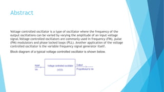
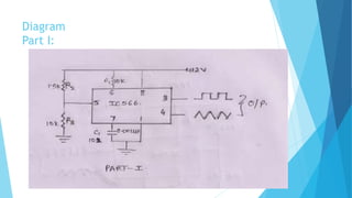
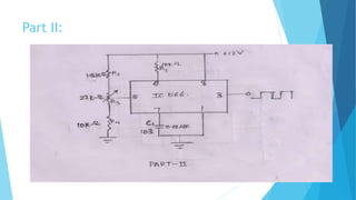
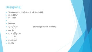
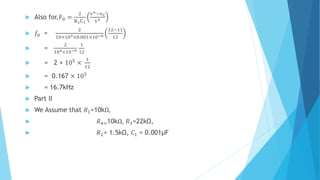
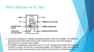
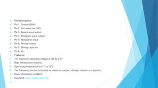
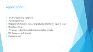
Study of VCO
Physics Department
Msc 1
Swapnil Barve
Neha Mannewar
Abstract
Voltage controlled oscillator is a type of oscillator where the frequency of the
output oscillations can be varied by varying the amplitude of an input voltage
signal.Voltage controlled oscillators are commonly used in frequency (FM), pulse
(PM) modulators and phase locked loops (PLL). Another application of the voltage
controlled oscillator is the variable frequency signal generator itself.
Block diagram of a typical voltage controlled oscillator is shown below.
Introduction
 LM566 is a monolithic voltage controlled oscillator from National
semiconductors. It can be used to generates square and triangle waveforms
simultaneously.
 The frequency of the output waveform can be adjusted using an external
control voltage.
 The output frequency can be also programmed using a set of external resistor
and capacitor.
 Typical applications of LM566 IC are signal generators, FM modulators, FSK
modulators, tone generators etc.
 While using single supply, the supply voltage range is from 10V to 24V. The IC
has a very linear modulation characteristics and has excellent thermal
stability.
Diagram
Part I:
Part II:
Working:
 IC566 contains current sources to charge and discharge an external capacitor at rate set by an
external resisitor R1 and the modulating DC input voltage V.
 A 0.001 uf capacitor is connected to pin5 and pin6. A Schmitt trigger circuit is used to switch
current sources between charging and discharging and the triangular voltage produced accross
the capacitor and square wave from scmitt trigger action are provided as outputs through
buffer amplifiers
 The Schmitt trigger swiches the current from charging and discharging the capacitor
 The IC charges and discharges the external capacitorC1 through external resistor R1. A
traingular waveform is obtained by passing the voltage accross the Capacitor C1 through
buffer amplifier 2 and obtained as output through pin4
 The voltage waveform accross the capacitor when passed through a Schmitt trigger which
passed through Buffer amplifier1 produces square waveform at pin 3
 Modulating voltage Vcc should be in range of 3/4Vcc <Vc<Vcc where Vcc is supply DC voltage
 Vcc should be on range of 10 - 24 volts.
 VCO is commonly used in low-frequency signals such as ECG (Electrocardiograms) into an audio
frequency range.

Designing:
 We assume 𝑅1= 10 kΩ, 𝑅3= 10 kΩ, 𝑅2= 1.5 kΩ
 𝐶1= 0.001µF
 𝑉+
= +12V

 We have,
 𝑣𝑐 =
𝑅3
𝑅2+𝑅3
𝑣+
(By Voltage Divider Theorem)
 And So,
 𝑉𝑐 =
10
1⋅5+10
× 12
 =
120
11⋅5
 𝑉𝑐= 10.4347
 𝑉𝑐≈ 11V
 Also for,F0 =
2
R1C1
v+−vC
v+
 𝑓0 =
2
10×103×0.001×10−6
12−11
12
 =
2
104×10−9
1
12
 = 2 × 105 ×
1
12
 = 0.167 × 10⁵
 = 16.7kHz
 Part II
 We Assume that 𝑅1=10kΩ,
 𝑅4=10kΩ, 𝑅3=22kΩ,
 𝑅2= 1.5kΩ, 𝐶1 = 0.001µF
Observation Table:
 Part I:
Types of Wave Time Amplitude Frequency
Square wave
Triangular wave
 Part II:
Sr.
No
Value of 𝑅3 Types of
Wave
Amplitude Time(T) Frequency
𝑓0
1 Sqaure
2 Sqaure
3 Sqaure
Trace:
T= 2 * 10µs
A=1* 5v
T= 3.4 * 10µs
A= 6v
Block Diagram of IC 566:
 A practical example of a voltage controlled oscillator (VCO) is the LM566. The LM566 is a
general purpose VCO which may be used to generate square wave and triangular
waveforms as a function input voltage.
 The LM566 is specified for operation over 0˚C to 70˚C temperature range. The frequency
of which is a linear function of a controlling voltage. The frequency is also controlled by
an external resistor and capacitor, whose values control the free running frequency.
 Pin Description:
 Pin 1: Ground (GND)
 Pin 2: No connection (NC)
 Pin 3: Square wave output
 Pin 4: Triangular wave output
 Pin 5: Modulation input
 Pin 6: Timing resistor
 Pin 7: Timing capacitor
 Pin 8: Vcc
 Features:
 The maximum operating voltage is 10V to 24V
 High temperature stability
 Operating temperature is 0˚C to 70˚C
 The frequency can be controlled by means of current, voltage, resistor or capacitor
 Power dissipation is 300mV
 Excellent power supply rejection

Application:
 Electronic jamming equipment.
 Function generator.
 Production of electronic music, for production of different types of noise.
 Phase locked loop.
 Frequency synthesizers, used in communication circuits.
 FSK (Frequency shift keying)
 Clock generator

Study of vco_Voltage controlled Oscillator

  • 1.
    Study of VCO PhysicsDepartment Msc 1 Swapnil Barve Neha Mannewar
  • 2.
    Abstract Voltage controlled oscillatoris a type of oscillator where the frequency of the output oscillations can be varied by varying the amplitude of an input voltage signal.Voltage controlled oscillators are commonly used in frequency (FM), pulse (PM) modulators and phase locked loops (PLL). Another application of the voltage controlled oscillator is the variable frequency signal generator itself. Block diagram of a typical voltage controlled oscillator is shown below.
  • 3.
    Introduction  LM566 isa monolithic voltage controlled oscillator from National semiconductors. It can be used to generates square and triangle waveforms simultaneously.  The frequency of the output waveform can be adjusted using an external control voltage.  The output frequency can be also programmed using a set of external resistor and capacitor.  Typical applications of LM566 IC are signal generators, FM modulators, FSK modulators, tone generators etc.  While using single supply, the supply voltage range is from 10V to 24V. The IC has a very linear modulation characteristics and has excellent thermal stability.
  • 4.
  • 5.
  • 6.
  • 7.
     IC566 containscurrent sources to charge and discharge an external capacitor at rate set by an external resisitor R1 and the modulating DC input voltage V.  A 0.001 uf capacitor is connected to pin5 and pin6. A Schmitt trigger circuit is used to switch current sources between charging and discharging and the triangular voltage produced accross the capacitor and square wave from scmitt trigger action are provided as outputs through buffer amplifiers  The Schmitt trigger swiches the current from charging and discharging the capacitor  The IC charges and discharges the external capacitorC1 through external resistor R1. A traingular waveform is obtained by passing the voltage accross the Capacitor C1 through buffer amplifier 2 and obtained as output through pin4  The voltage waveform accross the capacitor when passed through a Schmitt trigger which passed through Buffer amplifier1 produces square waveform at pin 3  Modulating voltage Vcc should be in range of 3/4Vcc <Vc<Vcc where Vcc is supply DC voltage  Vcc should be on range of 10 - 24 volts.  VCO is commonly used in low-frequency signals such as ECG (Electrocardiograms) into an audio frequency range. 
  • 8.
    Designing:  We assume𝑅1= 10 kΩ, 𝑅3= 10 kΩ, 𝑅2= 1.5 kΩ  𝐶1= 0.001µF  𝑉+ = +12V   We have,  𝑣𝑐 = 𝑅3 𝑅2+𝑅3 𝑣+ (By Voltage Divider Theorem)  And So,  𝑉𝑐 = 10 1⋅5+10 × 12  = 120 11⋅5  𝑉𝑐= 10.4347  𝑉𝑐≈ 11V
  • 9.
     Also for,F0= 2 R1C1 v+−vC v+  𝑓0 = 2 10×103×0.001×10−6 12−11 12  = 2 104×10−9 1 12  = 2 × 105 × 1 12  = 0.167 × 10⁵  = 16.7kHz  Part II  We Assume that 𝑅1=10kΩ,  𝑅4=10kΩ, 𝑅3=22kΩ,  𝑅2= 1.5kΩ, 𝐶1 = 0.001µF
  • 10.
    Observation Table:  PartI: Types of Wave Time Amplitude Frequency Square wave Triangular wave
  • 11.
     Part II: Sr. No Valueof 𝑅3 Types of Wave Amplitude Time(T) Frequency 𝑓0 1 Sqaure 2 Sqaure 3 Sqaure
  • 12.
    Trace: T= 2 *10µs A=1* 5v T= 3.4 * 10µs A= 6v
  • 13.
    Block Diagram ofIC 566:  A practical example of a voltage controlled oscillator (VCO) is the LM566. The LM566 is a general purpose VCO which may be used to generate square wave and triangular waveforms as a function input voltage.  The LM566 is specified for operation over 0˚C to 70˚C temperature range. The frequency of which is a linear function of a controlling voltage. The frequency is also controlled by an external resistor and capacitor, whose values control the free running frequency.
  • 14.
     Pin Description: Pin 1: Ground (GND)  Pin 2: No connection (NC)  Pin 3: Square wave output  Pin 4: Triangular wave output  Pin 5: Modulation input  Pin 6: Timing resistor  Pin 7: Timing capacitor  Pin 8: Vcc  Features:  The maximum operating voltage is 10V to 24V  High temperature stability  Operating temperature is 0˚C to 70˚C  The frequency can be controlled by means of current, voltage, resistor or capacitor  Power dissipation is 300mV  Excellent power supply rejection 
  • 15.
    Application:  Electronic jammingequipment.  Function generator.  Production of electronic music, for production of different types of noise.  Phase locked loop.  Frequency synthesizers, used in communication circuits.  FSK (Frequency shift keying)  Clock generator