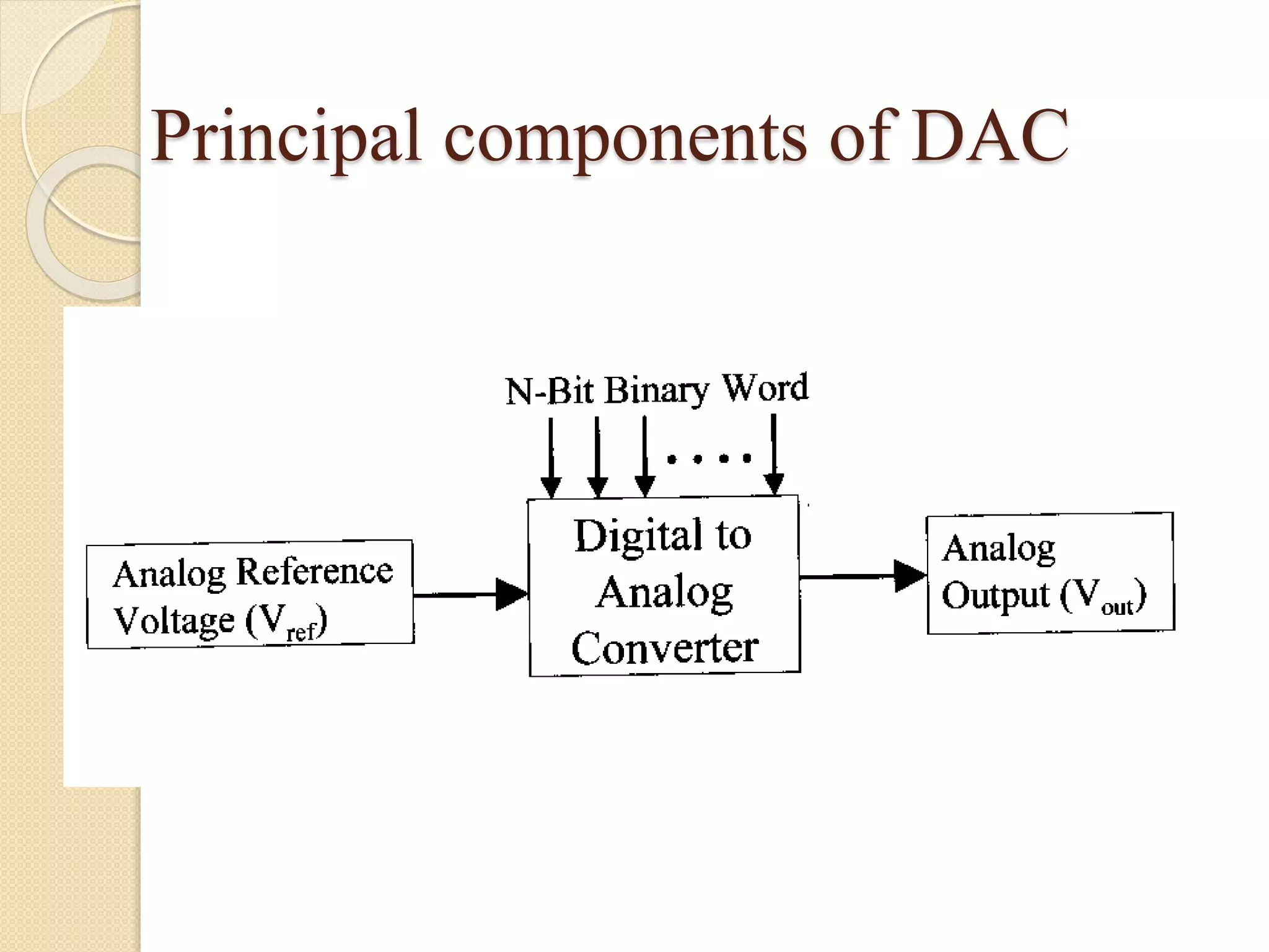
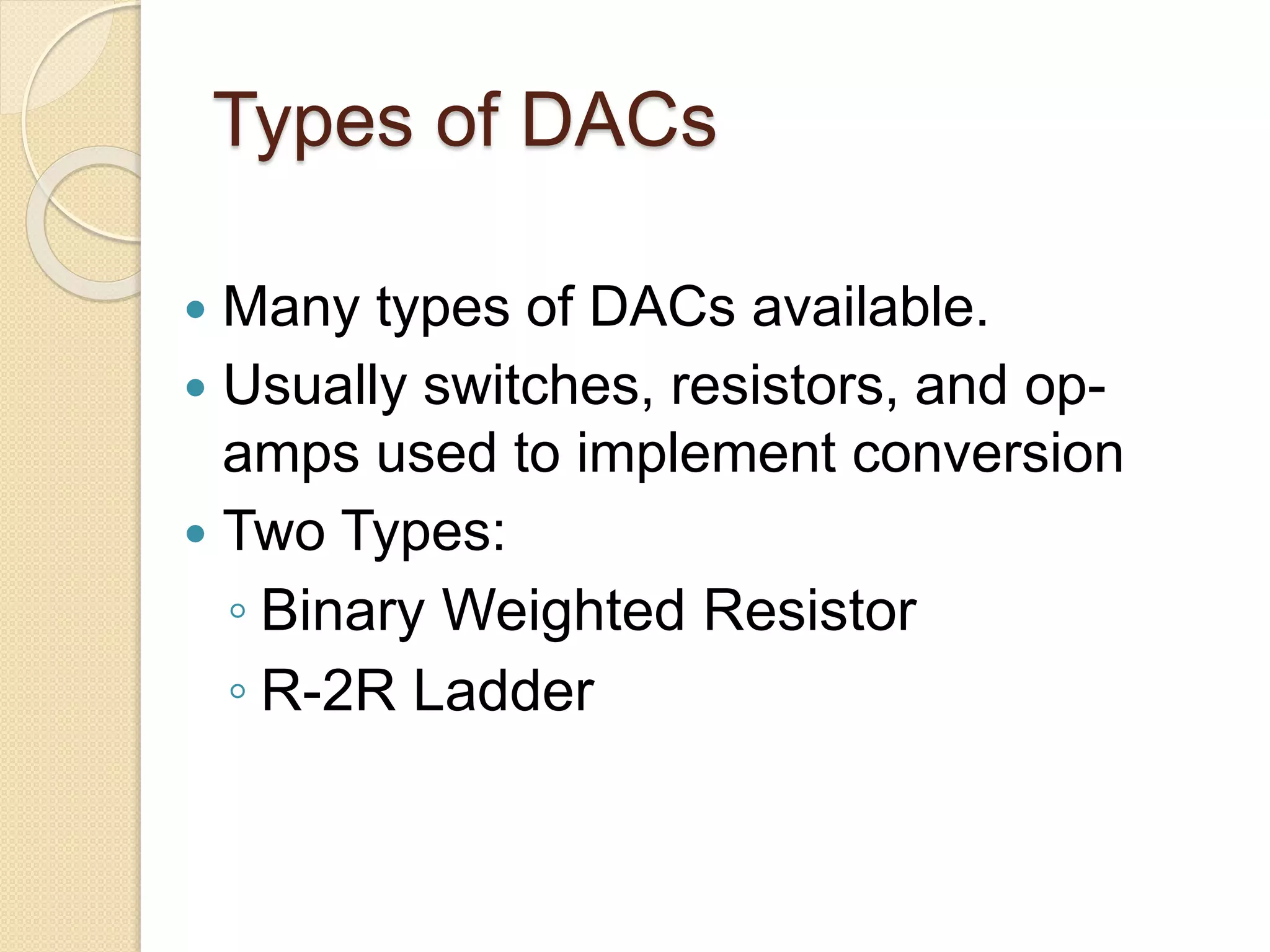
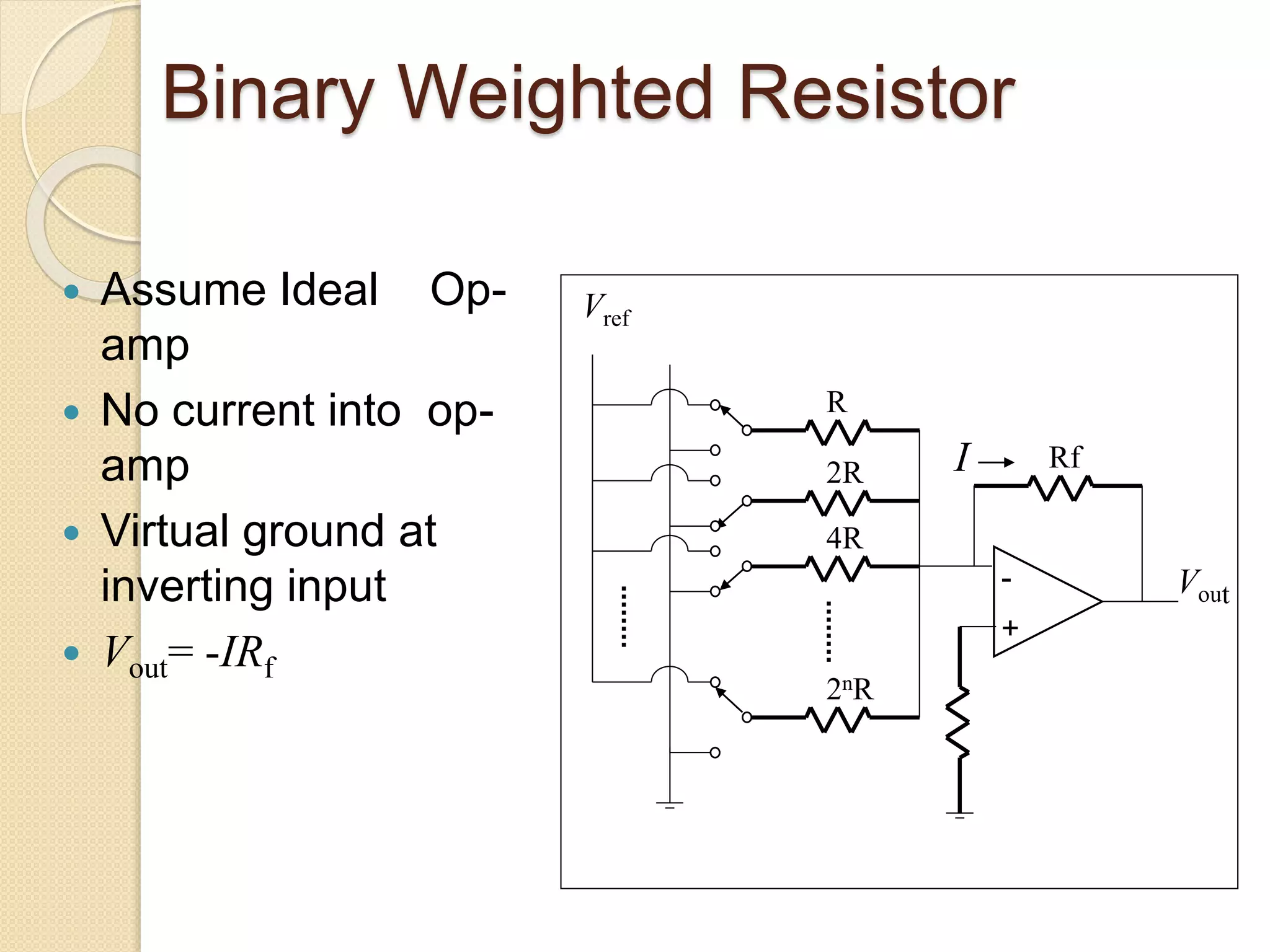
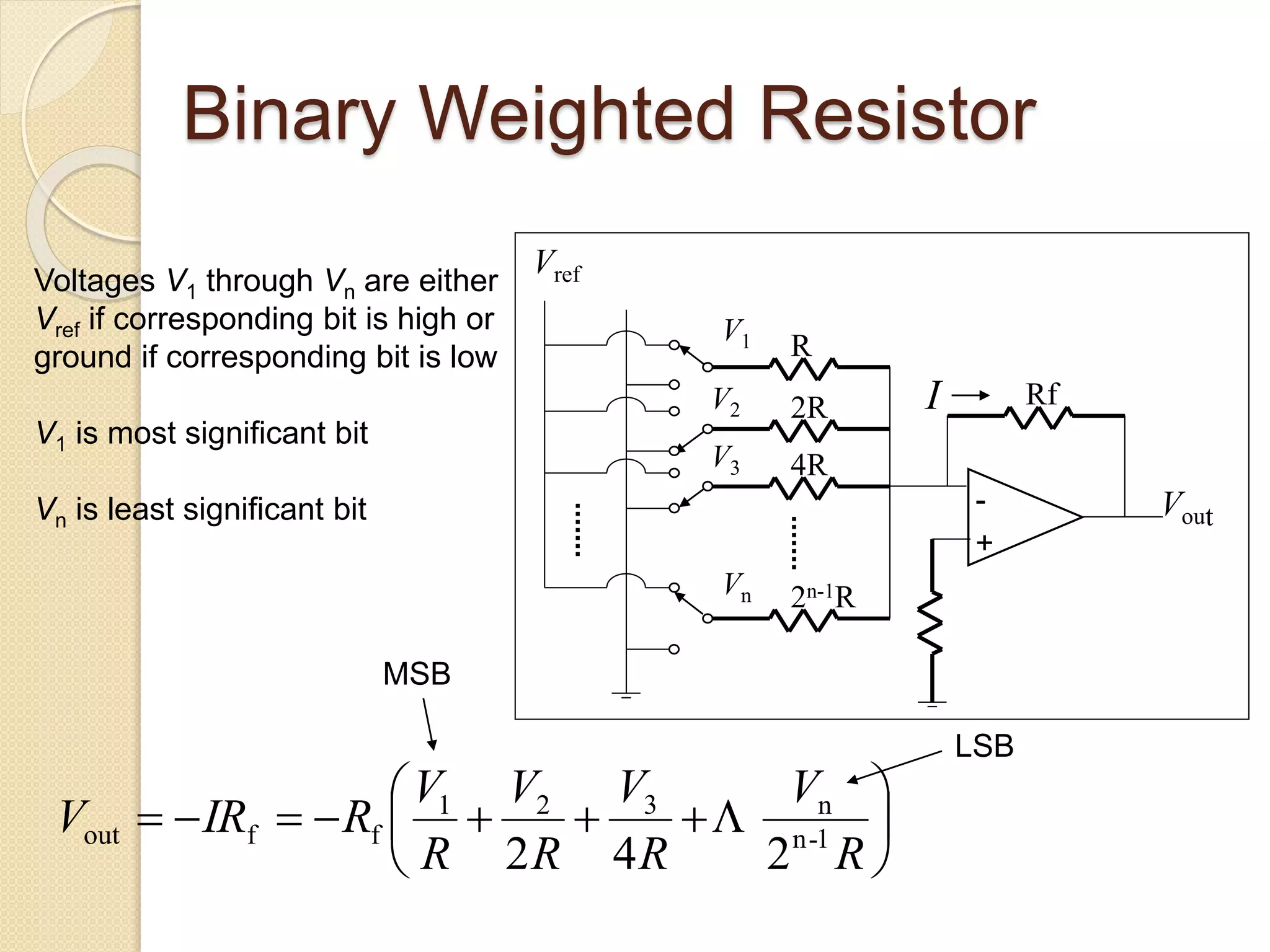
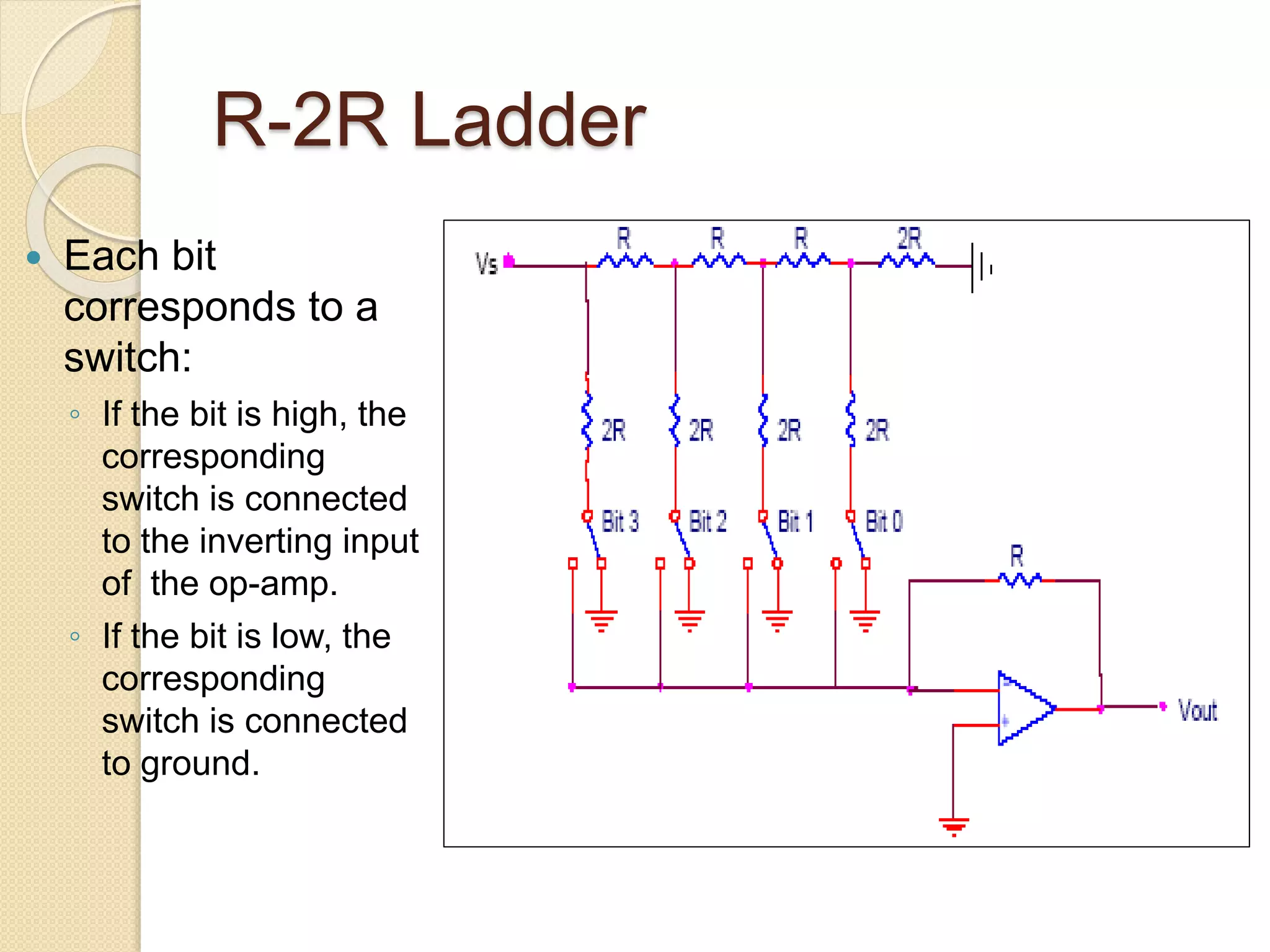
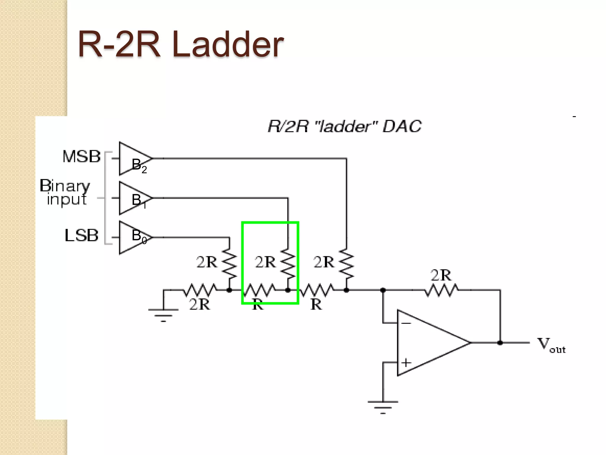
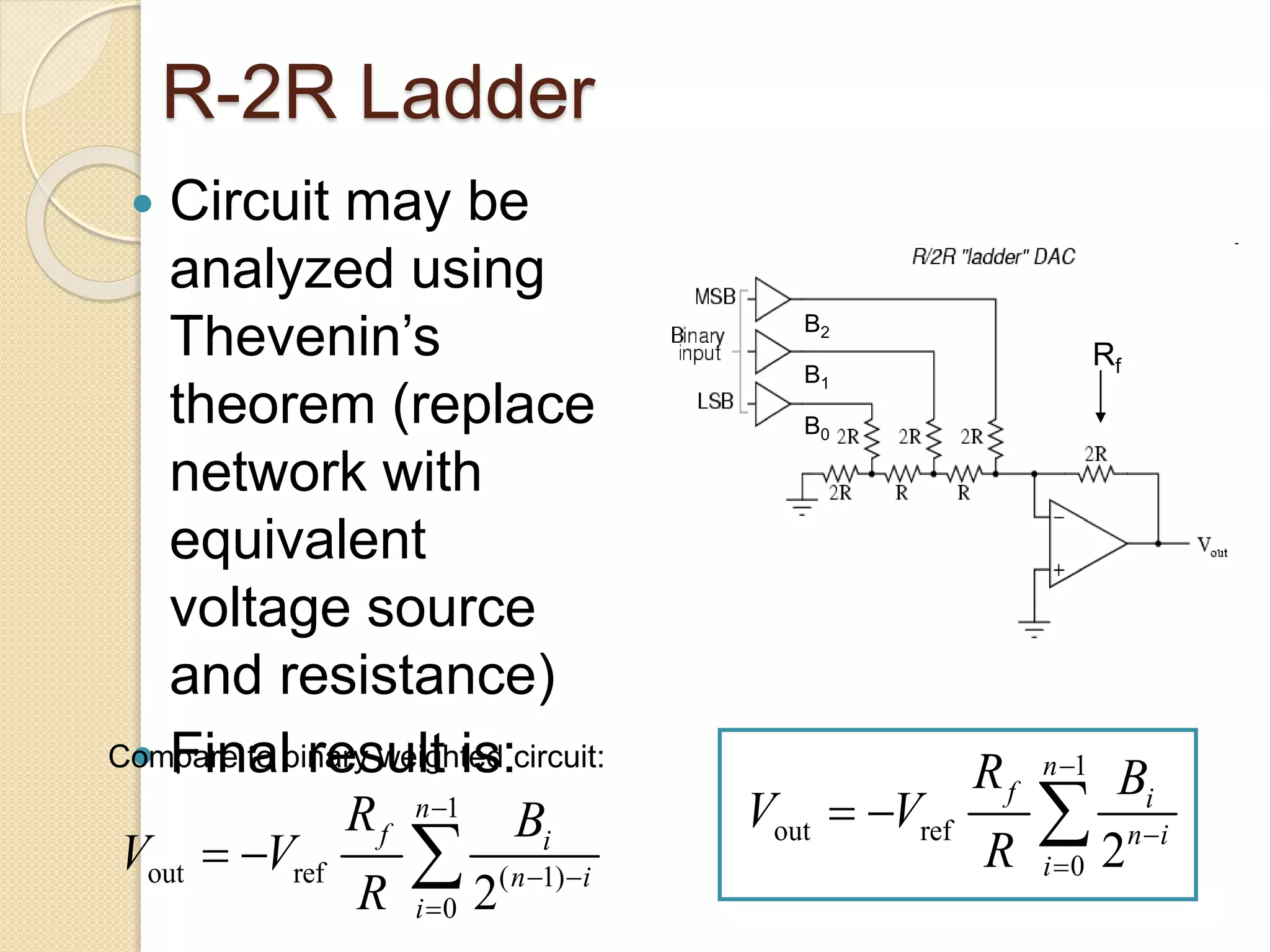
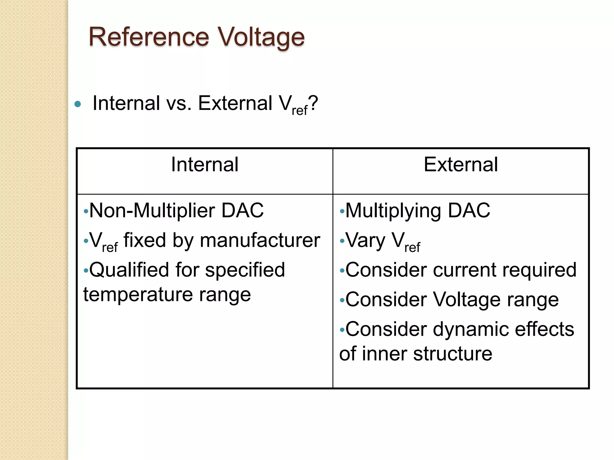
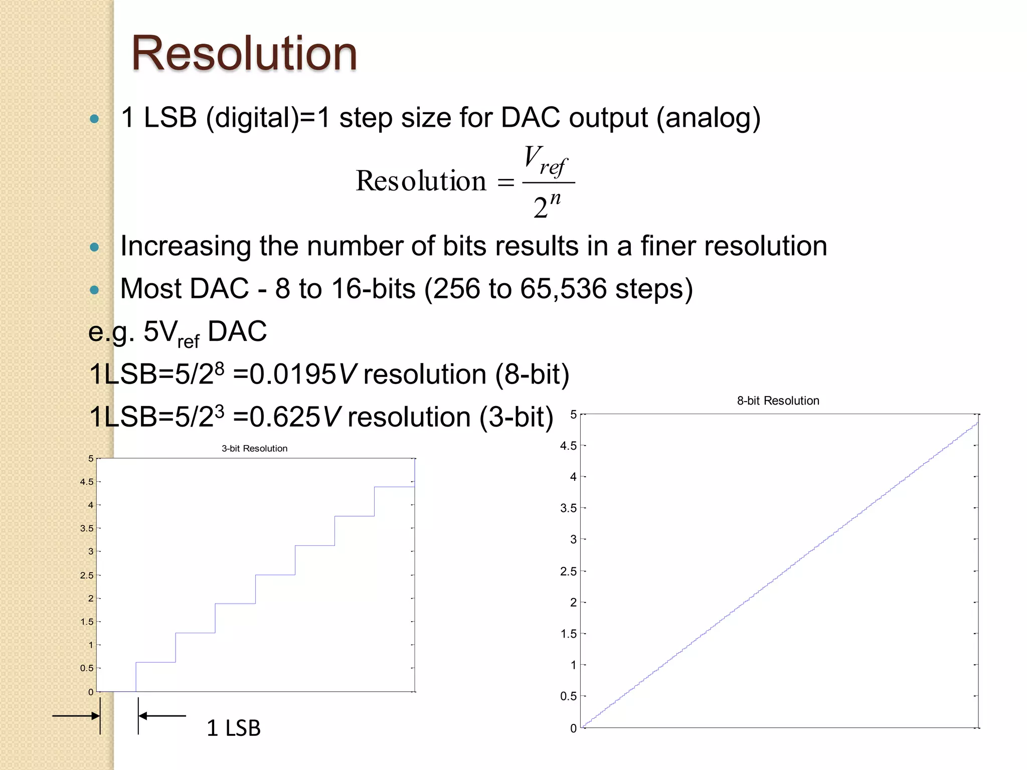
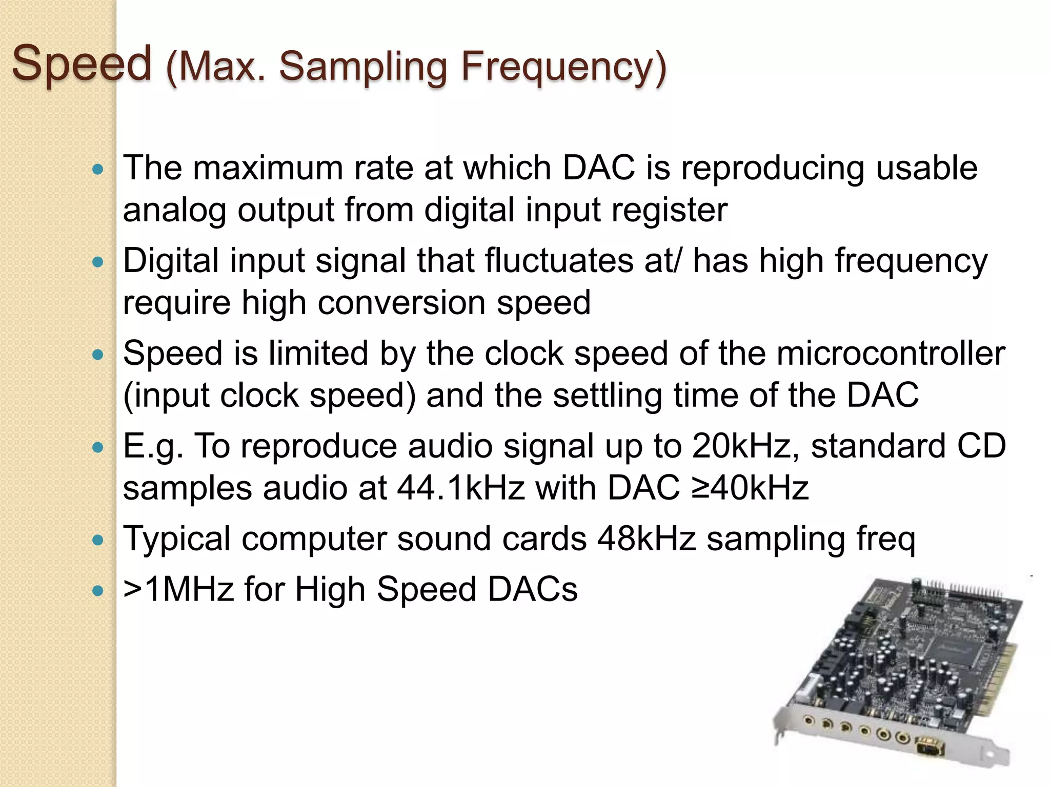
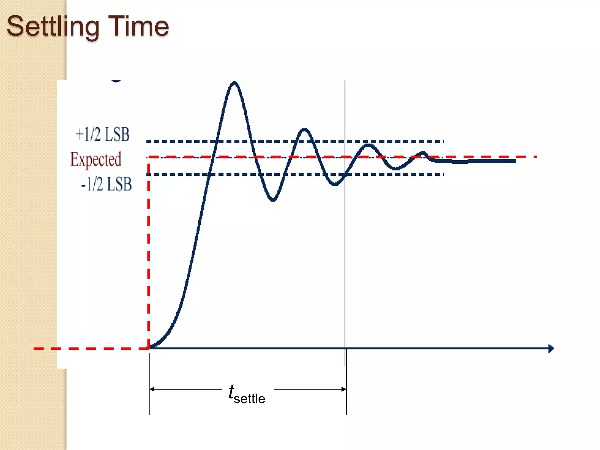
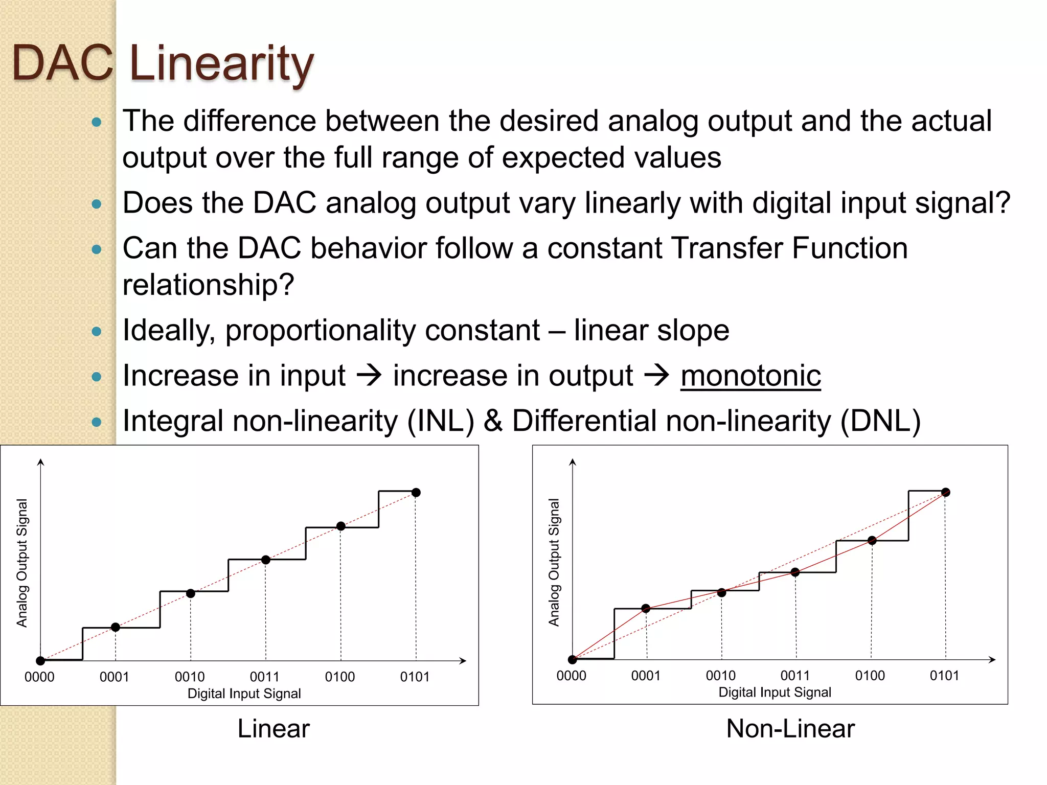
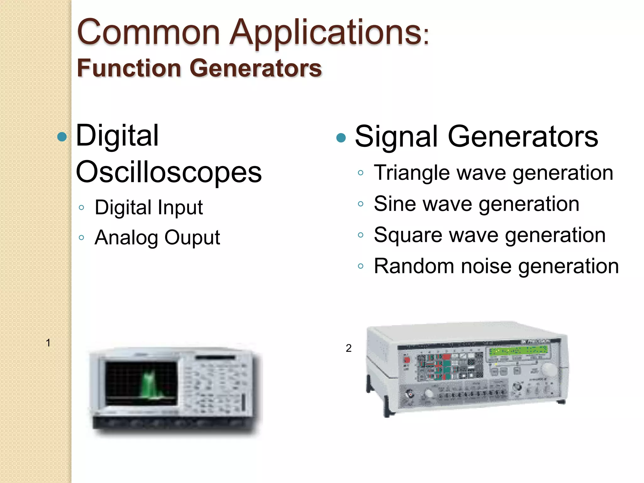
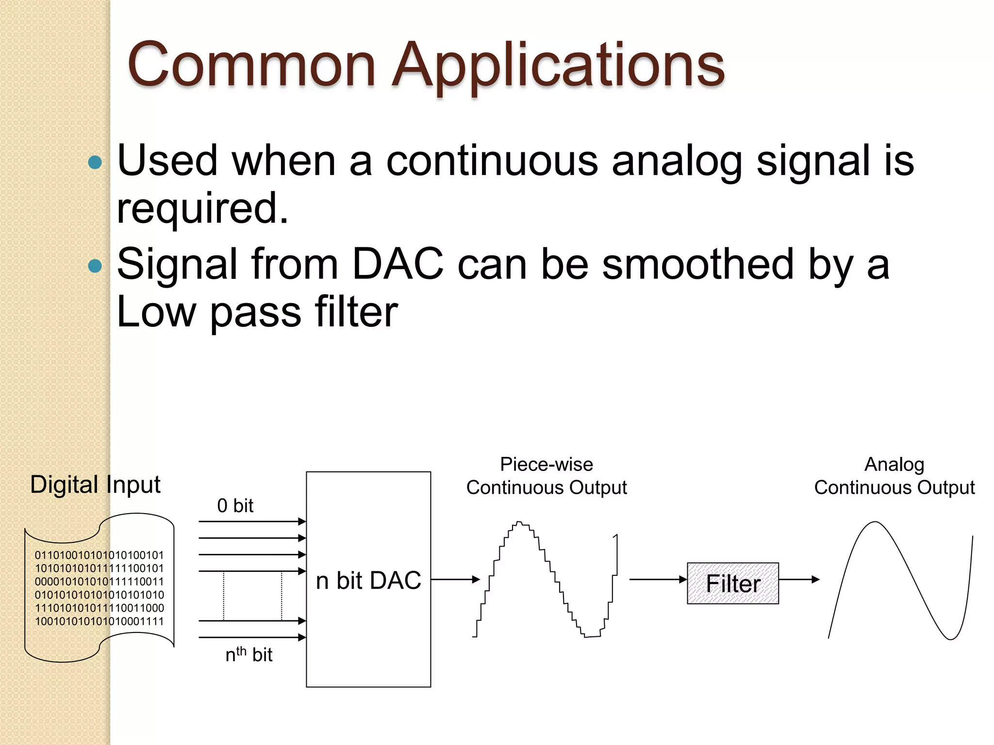
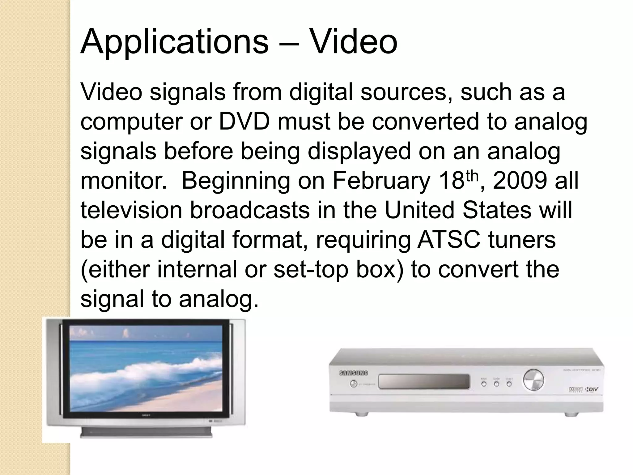
DIGITAL TO ANALOG
CONVERTER
Name : Gauravsinh Parmar
Enrollment no : 170410117023
What is a DAC?
 A digital to analog converter (DAC) is a device
that converts digital numbers (binary) into an
analog voltage or current output.
Principal components of DAC
What is a DAC?
 Digital  Analog
 Each binary number sampled by the DAC
corresponds to a different output level.
10111001 10100111 10000110010101000011001000010000
Digital Input Signal
AnalogOutputSignal
10111001 10100111 10000110010101000011001000010000
AnalogOutputSignal
Digital Input Signal
Types of DACs
 Many types of DACs available.
 Usually switches, resistors, and op-
amps used to implement conversion
 Two Types:
◦ Binary Weighted Resistor
◦ R-2R Ladder
Binary Weighted Resistor
 Utilizes a summing op-amp circuit
 Weighted resistors are used to
distinguish each bit from the most
significant to the least significant
 Transistors are used to switch
between Vref and ground (bit high or
low)
Binary Weighted Resistor
 Assume Ideal Op-
amp
 No current into op-
amp
 Virtual ground at
inverting input
 Vout= -IRf
-
+
R
2R
4R
2nR
Rf
Vout
I
Vref
Binary Weighted Resistor







R
V
R
V
R
V
R
V
RIRV 1-n
n321
ffout
242

MSB
LSB
Voltages V1 through Vn are either
Vref if corresponding bit is high or
ground if corresponding bit is low
V1 is most significant bit
Vn is least significant bit
I
-
+
R
2R
4R
2n-1R
Rf
Vout
Vref
V1
V2
V3
Vn
Binary Weighted Resistor
 Advantages
◦ Simple
◦ Fast
 Disadvantages
◦ Need large range of resistor values
(2048:1 for 12-bit) with high precision in
low resistor values
◦ Need very small switch resistances
◦ Op-amp may have trouble producing low
currents at the low range of a high
precision DAC
R-2R Ladder
 Each bit
corresponds to a
switch:
◦ If the bit is high, the
corresponding
switch is connected
to the inverting input
of the op-amp.
◦ If the bit is low, the
corresponding
switch is connected
to ground.
R-2R Ladder
B2
B1
B0
R-2R Ladder
 Circuit may be
analyzed using
Thevenin’s
theorem (replace
network with
equivalent
voltage source
and resistance)
 Final result is: 1
out ref
0 2
n
f i
n i
i
R B
V V
R



  
B2
B1
B0
Rf
Compare to binary weighted circuit:
1
out ref ( 1)
0 2
n
f i
n i
i
R B
V V
R

 

  
R-2R Ladder
 Advantages:
◦ Only 2 resistor values
◦ Lower precision resistors acceptable
 Disadvantages
◦ Slower conversion rate
DAC Specifications:
 Reference Voltages
 Resolution
 Speed
 Settling Time
 Linearity
Reference Voltage
 Internal vs. External Vref?
Internal External
•Non-Multiplier DAC
•Vref fixed by manufacturer
•Qualified for specified
temperature range
•Multiplying DAC
•Vary Vref
•Consider current required
•Consider Voltage range
•Consider dynamic effects
of inner structure
Resolution
 1 LSB (digital)=1 step size for DAC output (analog)
 Increasing the number of bits results in a finer resolution
 Most DAC - 8 to 16-bits (256 to 65,536 steps)
e.g. 5Vref DAC
1LSB=5/28 =0.0195V resolution (8-bit)
1LSB=5/23 =0.625V resolution (3-bit)
n
refV
2
Resolution 
0
0.5
1
1.5
2
2.5
3
3.5
4
4.5
5
8-bit Resolution
0
0.5
1
1.5
2
2.5
3
3.5
4
4.5
5
3-bit Resolution
1 LSB
Speed (Max. Sampling Frequency)
 The maximum rate at which DAC is reproducing usable
analog output from digital input register
 Digital input signal that fluctuates at/ has high frequency
require high conversion speed
 Speed is limited by the clock speed of the microcontroller
(input clock speed) and the settling time of the DAC
 E.g. To reproduce audio signal up to 20kHz, standard CD
samples audio at 44.1kHz with DAC ≥40kHz
 Typical computer sound cards 48kHz sampling freq
 >1MHz for High Speed DACs
Settling Time
 The interval between a command to update (change) its
output value and the instant it reaches its final value,
within a specified percentage (± ½ LSB)
 Ideal DAC output would be sequence of impulses 
Instantaneous update
 Causes:
◦ Slew rate of output amplifier
◦ Amount of amplifier ringing and signal overshoot
 Faster DACs have shorter settling time
 Electronic switching  fast
 Amplifier settling time  dominant effect
Settling Time
tsettle
DAC Linearity
 The difference between the desired analog output and the actual
output over the full range of expected values
 Does the DAC analog output vary linearly with digital input signal?
 Can the DAC behavior follow a constant Transfer Function
relationship?
 Ideally, proportionality constant – linear slope
 Increase in input  increase in output  monotonic
 Integral non-linearity (INL) & Differential non-linearity (DNL)
010101000011001000010000
Digital Input Signal
AnalogOutputSignal
010101000011001000010000 010101000011001000010000
Digital Input Signal
AnalogOutputSignal
010101000011001000010000
Digital Input Signal
AnalogOutputSignal
010101000011001000010000 010101000011001000010000
Digital Input Signal
AnalogOutputSignal
Linear Non-Linear
Common Applications:
Function Generators
 Digital
Oscilloscopes
◦ Digital Input
◦ Analog Ouput
 Signal Generators
◦ Triangle wave generation
◦ Sine wave generation
◦ Square wave generation
◦ Random noise generation
1
2
Common Applications
 Used when a continuous analog signal is
required.
 Signal from DAC can be smoothed by a
Low pass filter
0 bit
nth bit
n bit DAC
011010010101010100101
101010101011111100101
000010101010111110011
010101010101010101010
111010101011110011000
100101010101010001111
Digital Input
Filter
Piece-wise
Continuous Output
Analog
Continuous Output
Applications – Video
Video signals from digital sources, such as a
computer or DVD must be converted to analog
signals before being displayed on an analog
monitor. Beginning on February 18th, 2009 all
television broadcasts in the United States will
be in a digital format, requiring ATSC tuners
(either internal or set-top box) to convert the
signal to analog.
Common Applications
Motor Controllers
 Cruise Control
 Valve Control
 Motor Control
1 2 3
Ditial to Analog Converter

Ditial to Analog Converter

  • 1.
    DIGITAL TO ANALOG CONVERTER Name: Gauravsinh Parmar Enrollment no : 170410117023
  • 2.
    What is aDAC?  A digital to analog converter (DAC) is a device that converts digital numbers (binary) into an analog voltage or current output.
  • 3.
  • 4.
    What is aDAC?  Digital  Analog  Each binary number sampled by the DAC corresponds to a different output level. 10111001 10100111 10000110010101000011001000010000 Digital Input Signal AnalogOutputSignal 10111001 10100111 10000110010101000011001000010000 AnalogOutputSignal Digital Input Signal
  • 5.
    Types of DACs Many types of DACs available.  Usually switches, resistors, and op- amps used to implement conversion  Two Types: ◦ Binary Weighted Resistor ◦ R-2R Ladder
  • 6.
    Binary Weighted Resistor Utilizes a summing op-amp circuit  Weighted resistors are used to distinguish each bit from the most significant to the least significant  Transistors are used to switch between Vref and ground (bit high or low)
  • 7.
    Binary Weighted Resistor Assume Ideal Op- amp  No current into op- amp  Virtual ground at inverting input  Vout= -IRf - + R 2R 4R 2nR Rf Vout I Vref
  • 8.
    Binary Weighted Resistor        R V R V R V R V RIRV1-n n321 ffout 242  MSB LSB Voltages V1 through Vn are either Vref if corresponding bit is high or ground if corresponding bit is low V1 is most significant bit Vn is least significant bit I - + R 2R 4R 2n-1R Rf Vout Vref V1 V2 V3 Vn
  • 9.
    Binary Weighted Resistor Advantages ◦ Simple ◦ Fast  Disadvantages ◦ Need large range of resistor values (2048:1 for 12-bit) with high precision in low resistor values ◦ Need very small switch resistances ◦ Op-amp may have trouble producing low currents at the low range of a high precision DAC
  • 10.
    R-2R Ladder  Eachbit corresponds to a switch: ◦ If the bit is high, the corresponding switch is connected to the inverting input of the op-amp. ◦ If the bit is low, the corresponding switch is connected to ground.
  • 11.
  • 12.
    R-2R Ladder  Circuitmay be analyzed using Thevenin’s theorem (replace network with equivalent voltage source and resistance)  Final result is: 1 out ref 0 2 n f i n i i R B V V R       B2 B1 B0 Rf Compare to binary weighted circuit: 1 out ref ( 1) 0 2 n f i n i i R B V V R       
  • 13.
    R-2R Ladder  Advantages: ◦Only 2 resistor values ◦ Lower precision resistors acceptable  Disadvantages ◦ Slower conversion rate
  • 14.
    DAC Specifications:  ReferenceVoltages  Resolution  Speed  Settling Time  Linearity
  • 15.
    Reference Voltage  Internalvs. External Vref? Internal External •Non-Multiplier DAC •Vref fixed by manufacturer •Qualified for specified temperature range •Multiplying DAC •Vary Vref •Consider current required •Consider Voltage range •Consider dynamic effects of inner structure
  • 16.
    Resolution  1 LSB(digital)=1 step size for DAC output (analog)  Increasing the number of bits results in a finer resolution  Most DAC - 8 to 16-bits (256 to 65,536 steps) e.g. 5Vref DAC 1LSB=5/28 =0.0195V resolution (8-bit) 1LSB=5/23 =0.625V resolution (3-bit) n refV 2 Resolution  0 0.5 1 1.5 2 2.5 3 3.5 4 4.5 5 8-bit Resolution 0 0.5 1 1.5 2 2.5 3 3.5 4 4.5 5 3-bit Resolution 1 LSB
  • 17.
    Speed (Max. SamplingFrequency)  The maximum rate at which DAC is reproducing usable analog output from digital input register  Digital input signal that fluctuates at/ has high frequency require high conversion speed  Speed is limited by the clock speed of the microcontroller (input clock speed) and the settling time of the DAC  E.g. To reproduce audio signal up to 20kHz, standard CD samples audio at 44.1kHz with DAC ≥40kHz  Typical computer sound cards 48kHz sampling freq  >1MHz for High Speed DACs
  • 18.
    Settling Time  Theinterval between a command to update (change) its output value and the instant it reaches its final value, within a specified percentage (± ½ LSB)  Ideal DAC output would be sequence of impulses  Instantaneous update  Causes: ◦ Slew rate of output amplifier ◦ Amount of amplifier ringing and signal overshoot  Faster DACs have shorter settling time  Electronic switching  fast  Amplifier settling time  dominant effect
  • 19.
  • 20.
    DAC Linearity  Thedifference between the desired analog output and the actual output over the full range of expected values  Does the DAC analog output vary linearly with digital input signal?  Can the DAC behavior follow a constant Transfer Function relationship?  Ideally, proportionality constant – linear slope  Increase in input  increase in output  monotonic  Integral non-linearity (INL) & Differential non-linearity (DNL) 010101000011001000010000 Digital Input Signal AnalogOutputSignal 010101000011001000010000 010101000011001000010000 Digital Input Signal AnalogOutputSignal 010101000011001000010000 Digital Input Signal AnalogOutputSignal 010101000011001000010000 010101000011001000010000 Digital Input Signal AnalogOutputSignal Linear Non-Linear
  • 21.
    Common Applications: Function Generators Digital Oscilloscopes ◦ Digital Input ◦ Analog Ouput  Signal Generators ◦ Triangle wave generation ◦ Sine wave generation ◦ Square wave generation ◦ Random noise generation 1 2
  • 22.
    Common Applications  Usedwhen a continuous analog signal is required.  Signal from DAC can be smoothed by a Low pass filter 0 bit nth bit n bit DAC 011010010101010100101 101010101011111100101 000010101010111110011 010101010101010101010 111010101011110011000 100101010101010001111 Digital Input Filter Piece-wise Continuous Output Analog Continuous Output
  • 23.
    Applications – Video Videosignals from digital sources, such as a computer or DVD must be converted to analog signals before being displayed on an analog monitor. Beginning on February 18th, 2009 all television broadcasts in the United States will be in a digital format, requiring ATSC tuners (either internal or set-top box) to convert the signal to analog.
  • 24.
    Common Applications Motor Controllers Cruise Control  Valve Control  Motor Control 1 2 3