Download to read offline


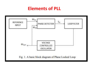


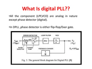


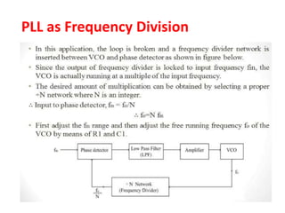


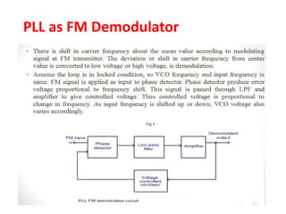


The document discusses phase-locked loops (PLLs), detailing their structure, components (including phase detector, loop filter, and voltage-controlled oscillator), and both analog and digital types of PLLs. It explains the function of various components and their interconnections, highlighting the applications of PLLs such as frequency synthesis, division, multiplication, and FM demodulation. The document emphasizes the importance of PLLs in tracking input signals and filtering out jitter.