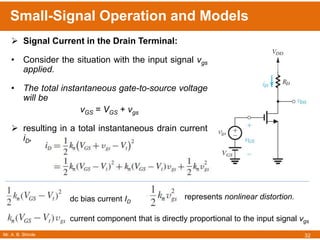
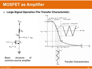
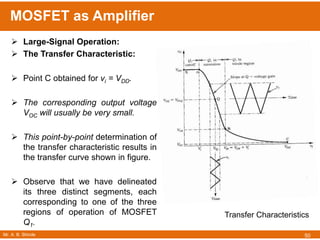
Downloaded 656 times
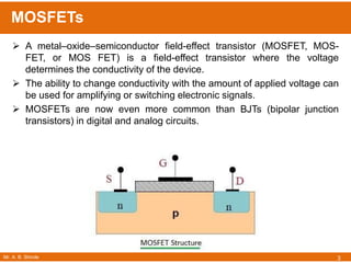
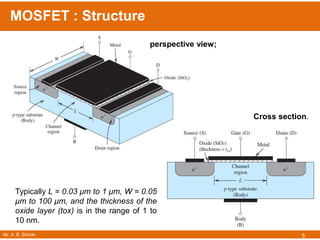
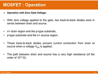
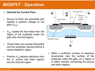
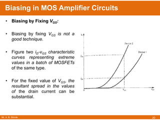

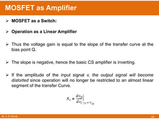
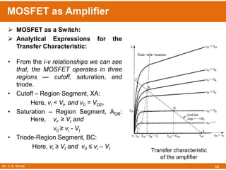

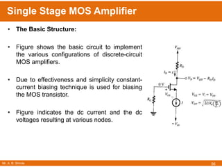

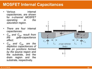


The document discusses MOSFETs (metal-oxide-semiconductor field-effect transistors). It provides information on: 1) The structure of MOSFETs including typical dimensions of the gate length and width. It operates by using a voltage applied to the gate to control the conductivity between the drain and source. 2) The operation of n-channel and p-channel MOSFETs. In an n-channel MOSFET, applying a positive voltage to the gate creates an n-type inversion channel between the source and drain allowing current to flow. 3) Biasing techniques for MOSFET amplifiers including fixing the gate voltage, connecting a resistor in the source,