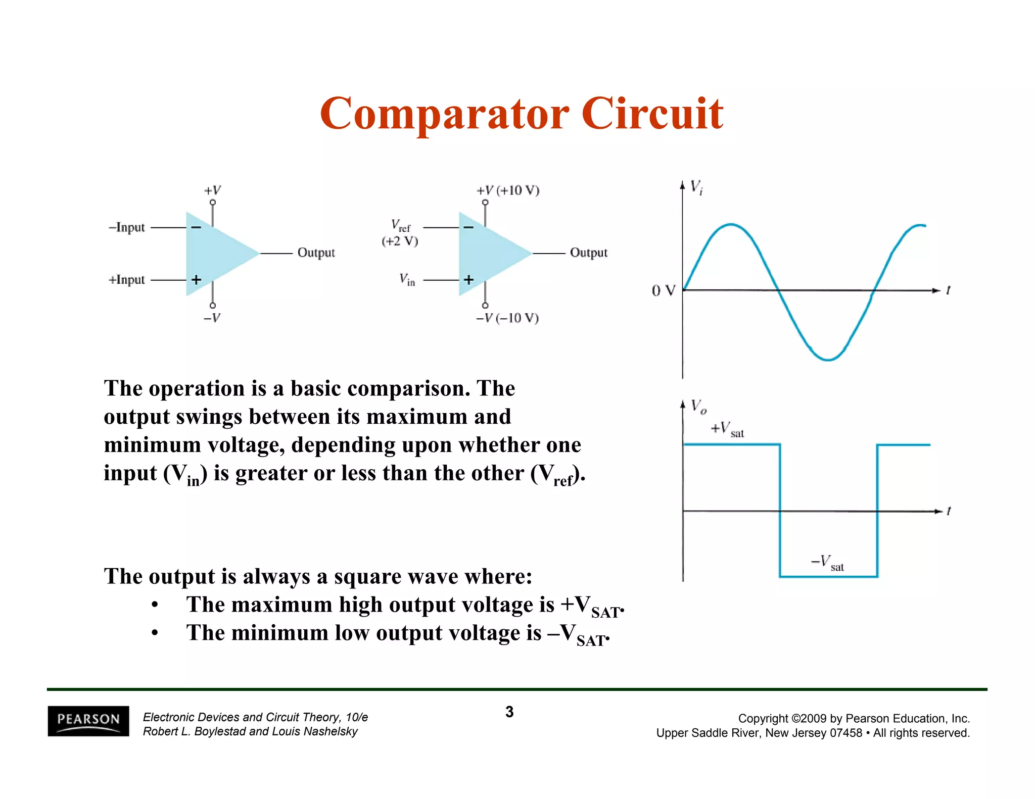
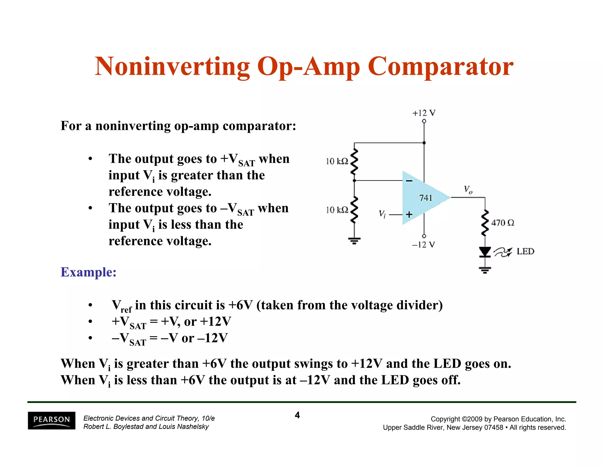
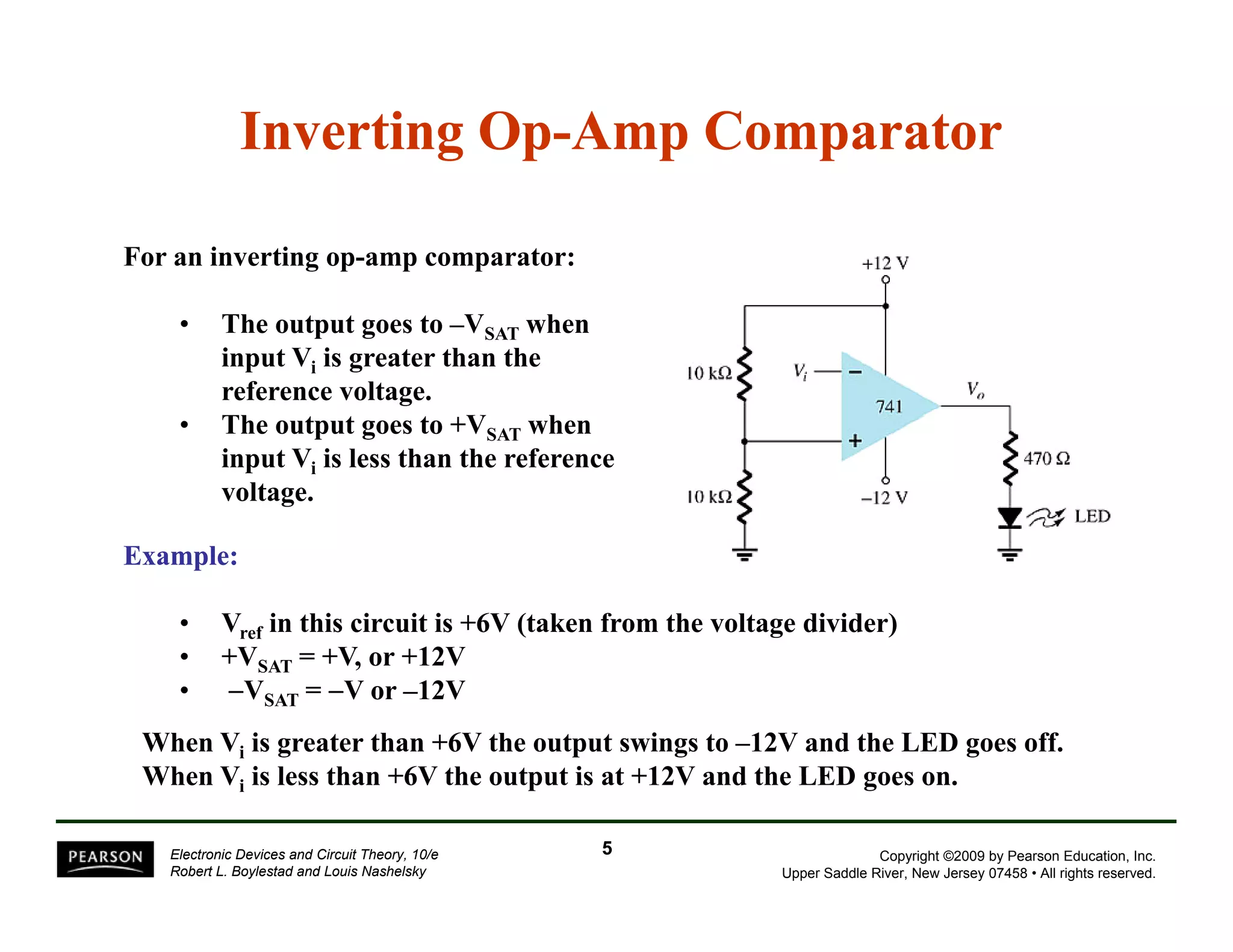
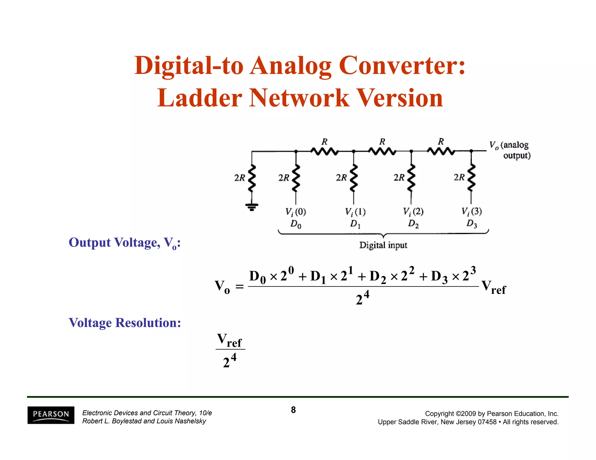
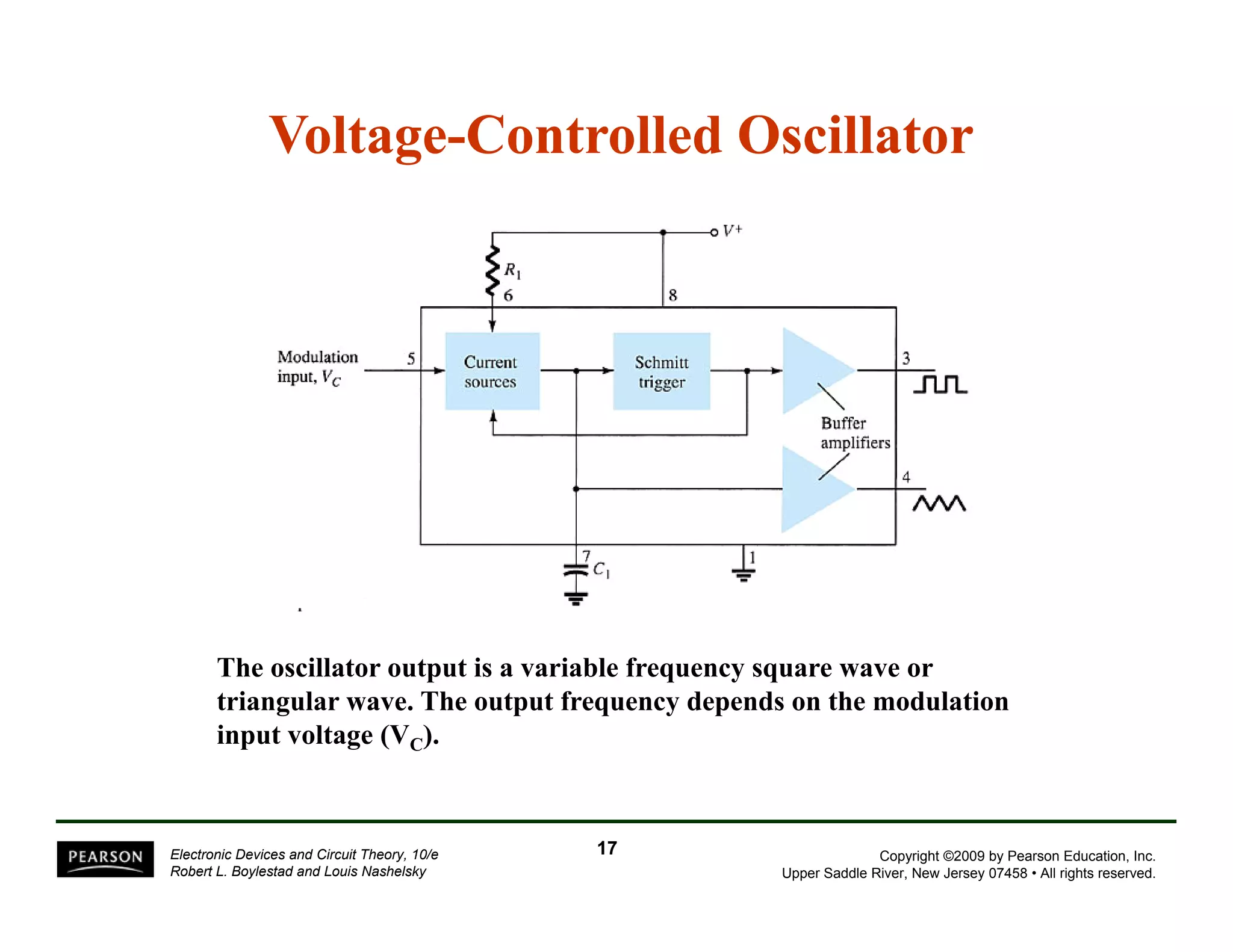
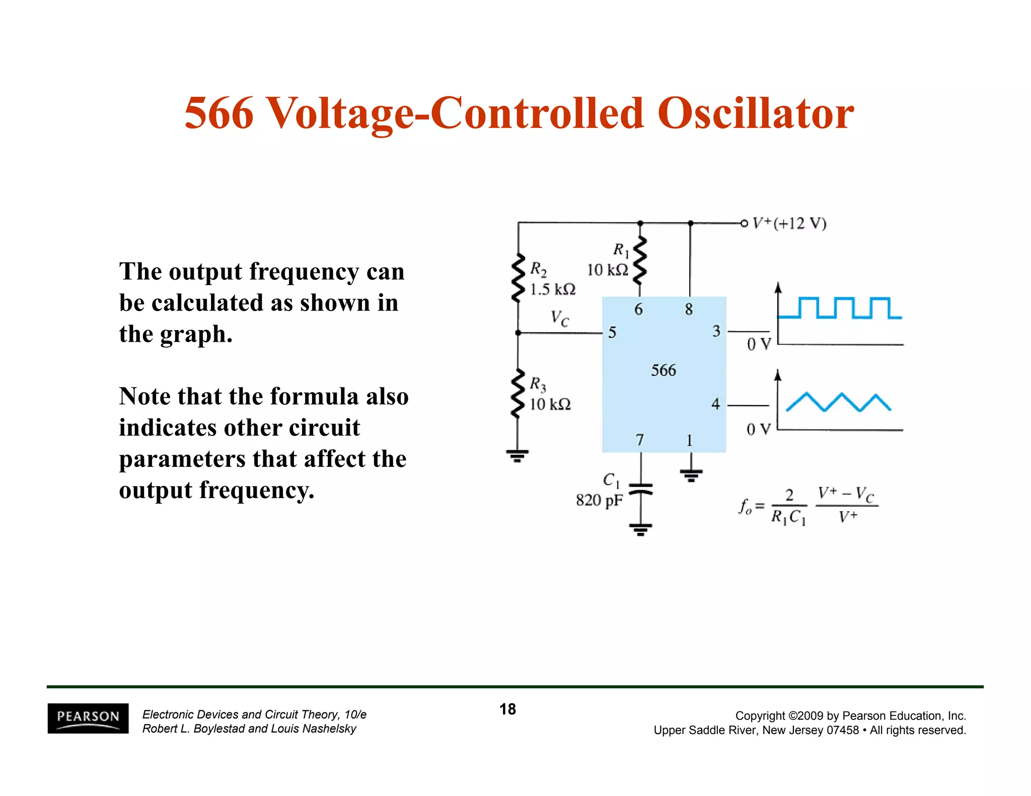
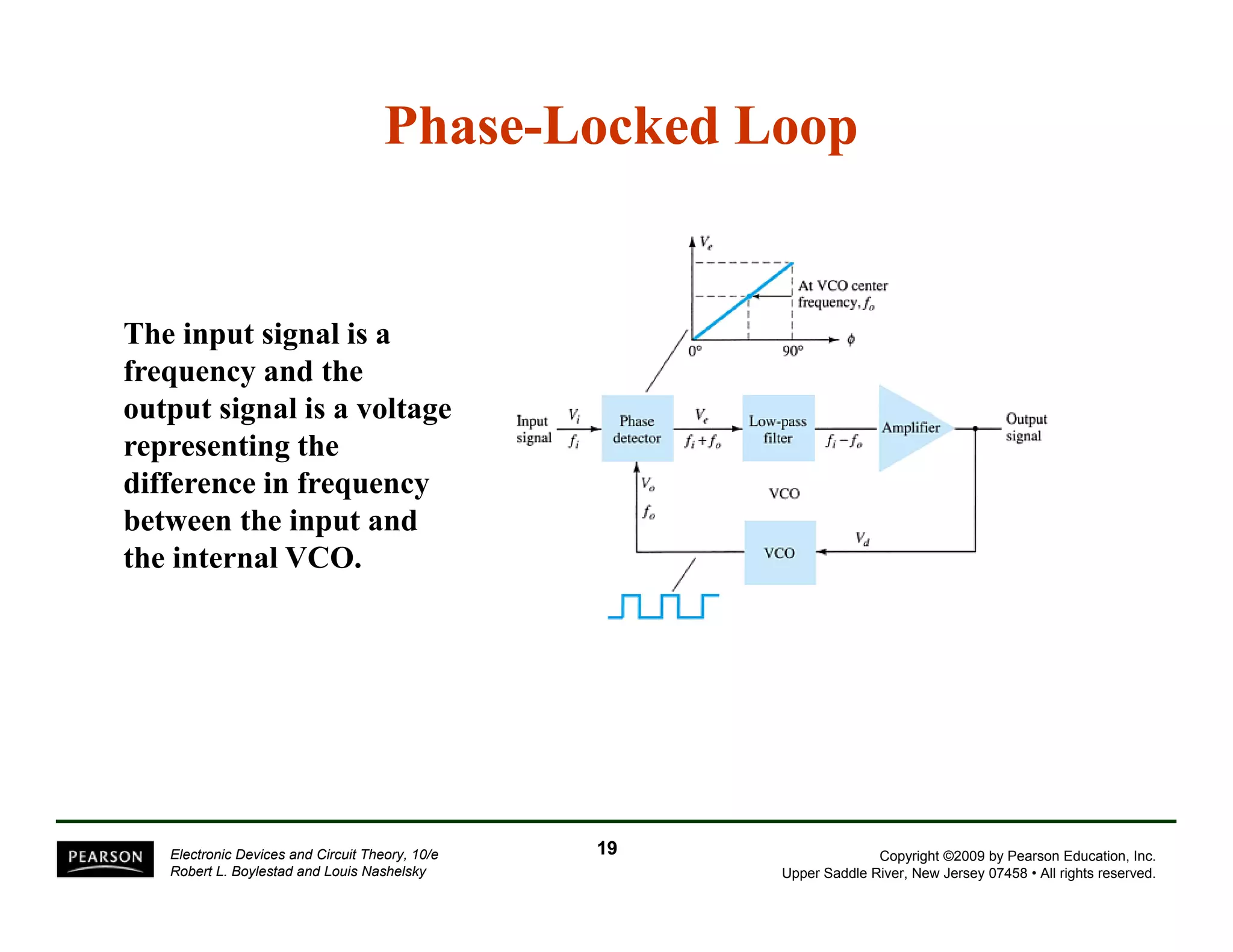
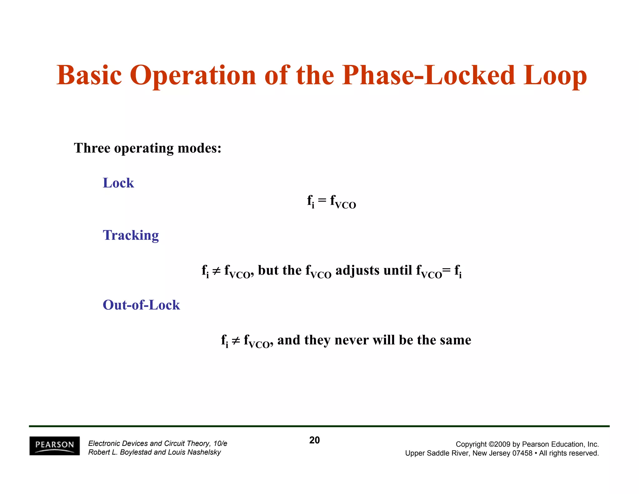
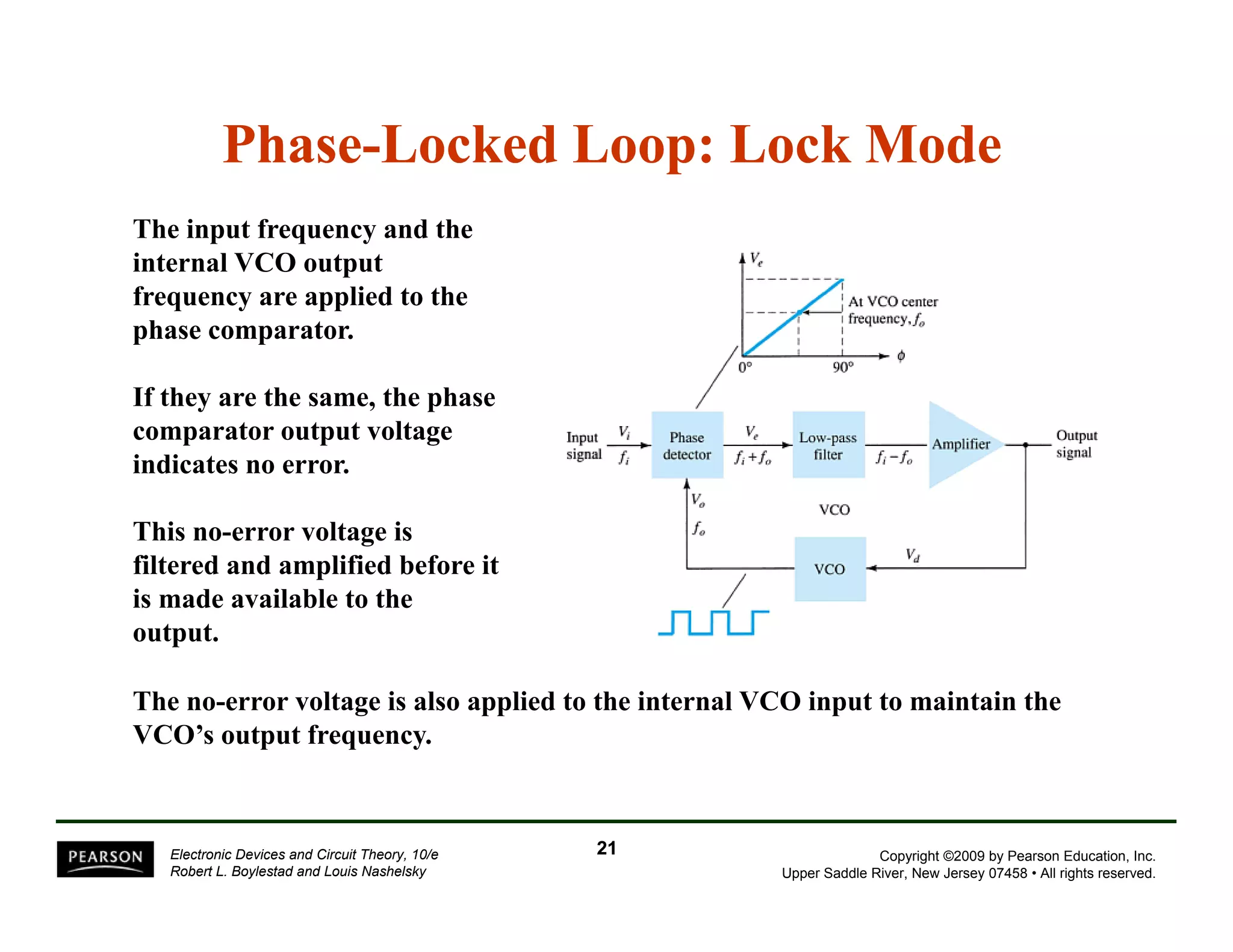
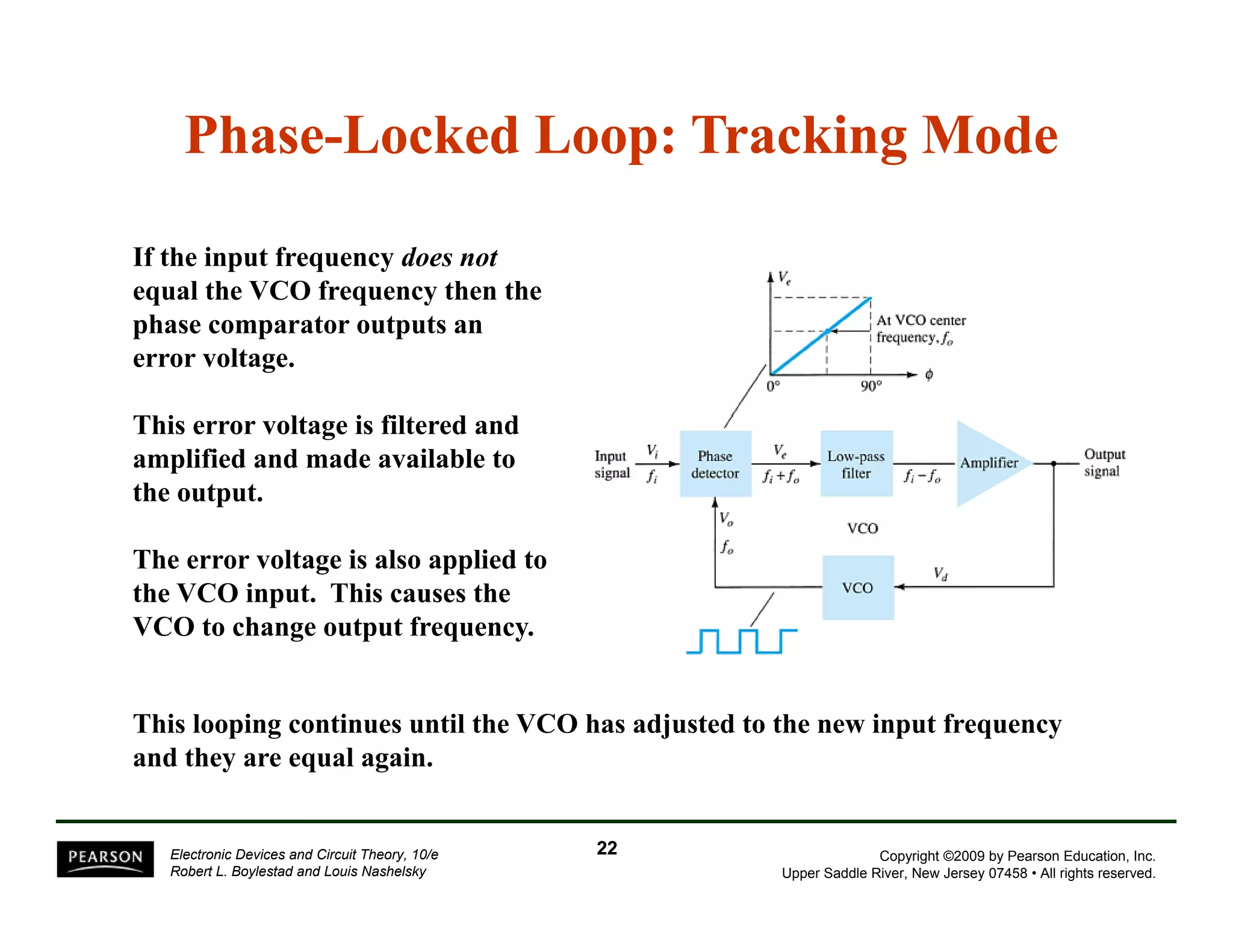
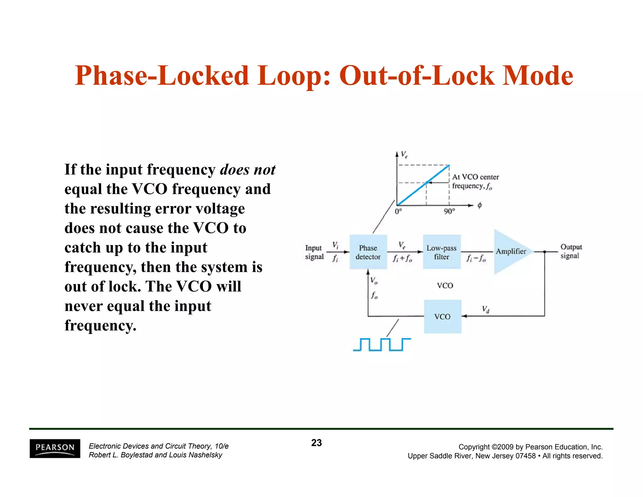
This document summarizes various linear-digital integrated circuits (ICs). It discusses comparators, digital-analog and analog-digital converters, timers, voltage-controlled oscillators, and phase-locked loop circuits. Comparators compare input voltages and output a high or low voltage. Digital converters translate between digital and analog formats while timers produce timed output pulses. Voltage-controlled oscillators vary output frequency with input voltage and phase-locked loops synchronize an oscillator's frequency to an input reference signal.
This document discusses various op-amp applications including constant-gain amplifiers, voltage summing, voltage buffers, controlled sources, instrumentation circuits, and active filters. It provides circuit diagrams and equations for calculating gain, cutoff frequencies, and other parameters. Applications include non-inverting and inverting amplifiers, voltage followers, voltage-controlled voltage sources, and first-order high-pass, low-pass, and bandpass filters.
This document discusses different classes of power amplifiers. Class A amplifiers conduct over the full 360 degrees of the input cycle but have low efficiency around 25%. Class B amplifiers conduct over 180 degrees and have higher efficiency of 78.5% but require two transistors for a full output cycle. Class AB is a compromise between the two. Class C conducts less than 180 degrees and uses a tuned circuit for output. Class D is for digital signals and requires pulse conversion circuits. Transformer coupling can improve class A efficiency to 50% by spreading out voltage and current swings.
This chapter discusses various two-terminal devices including Schottky diodes, varactor diodes, power diodes, tunnel diodes, photodiodes, photoconductive cells, IR emitters, liquid crystal displays, solar cells, and thermistors. It provides brief descriptions of each device and their operating principles as well as common applications.
This chapter discusses FET amplifiers. It describes the common FET configurations including common-source, common-gate, and common-drain. It provides the small-signal models and defines terms like transconductance. It then gives the input and output impedances and voltage gain calculations for each configuration. Examples of biased circuits are also presented along with a troubleshooting guide.
This chapter discusses various biasing circuits used for field effect transistors (FETs). It describes fixed-bias, self-bias, and voltage divider bias configurations for JFETs and MOSFETs. The key steps to analyze self and voltage divider bias circuits are: 1) Plot the transistor transfer curve and bias line, 2) Find the Q-point where they intersect, 3) Use the Q-point values to calculate the other circuit voltages and currents. D-type MOSFET biasing is similar to JFET biasing, except they can operate with positive VGS values and higher ID values than IDSS.
This document discusses different methods of biasing BJT transistors, including fixed bias, emitter-stabilized bias, and voltage divider bias circuits. It explains how the DC bias voltages establish an operating point (Q-point) for the transistor in either the active, cutoff, or saturation regions. Load line analysis is used to determine the transistor's Q-point based on the bias circuit components and supply voltage. Feedback circuits are also introduced to improve stability against variations in the transistor's beta value.
This document summarizes BJT transistor modeling and analysis techniques. It discusses two common models for small signal AC analysis: the re model and hybrid equivalent model. It then focuses on analyzing the re model in various BJT configurations including common-emitter, common-base, and emitter follower. Calculation of gains, impedances, and voltages are demonstrated for each configuration. Feedback pair and current mirror circuits are also briefly introduced.
This document discusses power supplies and voltage regulators. It covers the components of typical power supplies, including rectifiers to convert AC to DC, filter circuits to reduce ripple voltage, and voltage regulator circuits to maintain a constant output voltage. Two common voltage regulator configurations are described: discrete transistor regulators and integrated circuit regulators. The document provides examples of series and shunt voltage regulator circuits and discusses fixed, adjustable, and negative voltage regulator ICs.
Operational amplifiers (op-amps) are high gain differential amplifiers with very high input impedance and low output impedance. Op-amps can be connected in either open-loop or closed-loop configurations, with closed-loop providing feedback to control and reduce the gain. Common op-amp circuits include inverting and non-inverting amplifiers, unity followers, summing amplifiers, integrators, and differentiators. Op-amps have specifications including input offset voltage and input offset current, which can cause an output offset even when the input is zero.
The document discusses the frequency response of BJT and FET amplifiers. It explains that at low frequencies, coupling and bypass capacitors lower the gain, while at high frequencies, stray capacitances associated with the active device lower the gain. The frequency range where an amplifier operates with negligible effects from capacitors is called the mid-range or bandwidth. Bode plots are used to illustrate the cutoff frequencies and roll-off of gain outside this bandwidth. The various factors that determine the low and high frequency cutoffs are analyzed.
The document discusses various applications of operational amplifiers (op-amps) including constant-gain amplifiers, voltage summing, voltage buffers, controlled sources, instrumentation circuits, and active filters. Op-amps can be used to create inverting and non-inverting amplifiers, sum voltages, buffer signals, and act as controlled sources for voltage or current. Instrumentation circuits include display drivers and instrumentation amplifiers. Active filters that can be created using op-amps include low-pass, high-pass, and bandpass filters by adding capacitors and resistors to filter voltages at certain cutoff frequencies.
1) An operational amplifier (op-amp) is a high-gain differential amplifier with very high input impedance and low output impedance. It has two input terminals (inverting and non-inverting) and one output terminal.
2) Op-amps can be connected in either open-loop or closed-loop configurations. Open-loop gain can exceed 10,000 but closed-loop with negative feedback reduces gain and improves characteristics.
3) Common op-amp circuits include inverting and non-inverting amplifiers, unity followers, summing amplifiers, integrators, and differentiators.
There are two types of transistors, PNP and NPN. A transistor has three terminals - emitter, base, and collector. In an NPN transistor, the emitter-base junction is forward biased and the base-collector junction is reverse biased. There are three common transistor configurations - common-base, common-emitter, and common-collector. The common-emitter configuration is most widely used. A transistor can be used to amplify signals and its gain is determined by its beta value. Transistors have defined operating regions and limits that depend on the configuration.
This document discusses feedback and oscillator circuits. It describes the effects of negative feedback on amplifiers, including lower gain but higher input impedance, more stable gain, improved frequency response, and lower output impedance. There are four types of feedback connections: voltage-series, voltage-shunt, current-series, and current-shunt. Oscillators require positive feedback where the overall gain equals one. Common oscillator circuits include phase-shift, Wien bridge, tuned, crystal, and unijunction oscillators.
This document discusses feedback amplifiers and their classifications. It describes four types of amplifiers: voltage amplifiers, current amplifiers, transconductance amplifiers, and transresistance amplifiers. It explains their characteristics and how they are defined based on input and output resistances. The document also introduces the concept of feedback, describing the basic components of a feedback loop including the signal source, feedback network, and sampling network. Feedback modifies the characteristics of an amplifier by combining a portion of the output signal with the external input signal.
This document discusses resonance in series and parallel RLC circuits. It defines key parameters for both circuit types including resonance frequency, half-power frequencies, bandwidth, and quality factor. The series resonance circuit is analyzed showing that impedance is purely resistive at resonance, with maximum current and unity power factor. Parallel resonance is also examined, with admittance being purely conductance at resonance. Formulas for calculating important resonant characteristics are provided.
The document summarizes key concepts about semiconductor diodes. It discusses how diodes are made from doped semiconductor materials like silicon and conduct current mainly in one direction. Diodes have different operating characteristics depending on whether they are forward biased, reverse biased, or at no bias. The document also covers diode testing methods and applications of diodes like in LEDs and zener diodes.
The document discusses ideal operational amplifiers and various op-amp circuits, including:
- Inverting and non-inverting amplifiers and their voltage gain formulas
- Summing and difference amplifiers
- Integrator and differentiator circuits
It provides examples of calculating the voltage gain for different op-amp configurations and designing circuits to meet specific output conditions. Concepts covered include open loop gain, input resistance, feedback resistance, and Kirchhoff's current law analysis.
This document discusses BJT amplifiers, including:
- The basics of bipolar junction transistors including construction, modes of operation, DC and small-signal models
- Single-stage BJT amplifier configurations including common-emitter, common-base, and common-collector amplifiers
- Graphical and small-signal analysis techniques for BJT amplifiers
- Key aspects like voltage gain, input and output impedances, and frequency response are examined for each configuration
The document discusses various applications of operational amplifiers as comparators and other circuits. It describes how op-amps can be used as zero-level detectors, nonzero-level detectors, and how hysteresis can reduce noise effects in comparators. It also discusses summing amplifiers, averaging amplifiers, scaling adders, and how op-amps can be configured as integrators and differentiators.
This document summarizes key concepts about BJT AC analysis from Chapter 5 of the textbook. It discusses two common models used for small signal AC analysis: the re model and hybrid equivalent model. The re model represents the BJT as a diode and current source and is designed for specific circuit conditions. It then provides details on analyzing several common BJT configurations, including common-emitter, using the re model, discussing input impedance, output impedance, voltage gain and current gain. It also briefly introduces the feedback pair and current mirror circuits.
- The document discusses first-order RC and RL circuits.
- Key aspects include: RC and RL circuits can be modeled with first-order differential equations; the natural response of source-free circuits decays exponentially with a time constant τ equal to RC or L/R.
- The energy initially stored in the capacitor or inductor is dissipated in the resistor over time according to an exponential function with the same time constant.
- Any steady state voltage or current in a linear circuit with a sinusoidal source is a sinusoid with the same frequency as the source. Phasors and complex impedances allow conversion of differential equations to circuit analysis by representing magnitude and phase of sinusoids.
- For a resistor, the voltage and current are in phase. In the phasor domain, the resistor phasor relationship is V=IR. In the time domain, the average power dissipated is proportional to the product of RMS current and voltage.
This document discusses root mean square (RMS) value, average value, form factor, and peak factor of alternating quantities. It defines each term and describes several methods to calculate RMS value and average value, including the mid-ordinate method and analytical method. For a sinusoidal waveform, the RMS value is 0.707 times the peak value, the average value is 0.637 times the peak value, the form factor is the ratio of RMS to average value (which is 1.11 for sinusoidal), and the peak factor is the ratio of peak value to RMS value (which is 1.414 for sinusoidal).
The document discusses Thevenin's theorem for AC networks. It defines Thevenin's theorem as stating that any linear AC network seen between two terminals can be replaced by a single voltage source (Vth) in series with a single impedance (Zth). It then provides steps to calculate the Thevenin equivalent circuit for a given network: 1) remove the load, 2) calculate the open circuit voltage Vth, 3) simplify the network, 4) calculate the input impedance Zth, and 5) replace the network with the equivalent Vth and Zth. An example network is also worked through as an illustration.
This chapter discusses impedance in alternating current circuits. It explains the characteristics and calculations for resistive-inductive and resistive-capacitive series circuits, including the phase relationships between voltage and current. Several example calculations of voltage, current, impedance and reactance in AC circuits are shown. The chapter concludes with a summary of key points and a preview of the next lesson.
This document discusses various diode applications including load line analysis, rectifier circuits, clipping circuits, and voltage multiplier circuits. Rectifier circuits such as half-wave, full-wave, and voltage doublers are used to convert AC to DC power. Clipping and clamping circuits use diodes to limit output voltages. Voltage multiplier circuits step up voltage using combinations of diodes and capacitors. Practical applications include battery charging, overvoltage protection, and setting reference voltages.
This document discusses Kirchoff's laws, which are two circuit analysis laws developed by Gustav Kirchoff in 1845. The first law, known as Kirchoff's voltage law (KVL), states that the sum of the voltages around any closed loop in a circuit is equal to zero. The second law, known as Kirchoff's current law (KCL), states that the algebraic sum of the currents at any node or junction in a circuit is equal to zero. The document provides examples of applying KVL and KCL, including using mesh analysis, and contains three review questions about Kirchoff's laws and circuit analysis techniques.
This document discusses various types of linear digital integrated circuits (ICs), including comparators, digital-to-analog and analog-to-digital converters, timers, voltage-controlled oscillators, and phase-locked loop circuits. It provides examples of comparator circuits, describes different types of converters and their operation, and explains how timers, voltage-controlled oscillators, and phase-locked loops work.
1. Power supplies use rectifier and filter circuits to convert AC voltage to DC voltage for use in electronic devices. Filter circuits reduce ripple voltage through the use of capacitors and RC networks.
2. There are two main types of voltage regulation circuits - discrete transistor circuits and integrated circuit regulators. Discrete regulators include series and shunt configurations while IC regulators provide fixed positive, fixed negative, or adjustable outputs with protection from overloads.
3. Voltage regulators, whether discrete transistor or IC-based, use a feedback loop to sample the output voltage and compare it to a reference voltage to control a series or shunt element to maintain a constant output voltage under varying load and line conditions.
Chapter 4 Boylstead DC Biasing-BJTs.pptxAneesSohail1
This document summarizes key concepts about biasing transistors, including:
1) Biasing establishes operating conditions like current and voltage to turn the transistor on for amplifying AC signals. Important to keep the operating point (Q-point) stable for proper transistor functioning.
2) Common biasing circuits include fixed bias, emitter-stabilized bias, voltage divider bias, and collector feedback. Emitter-stabilized and voltage divider biases are more stable against temperature and transistor parameter variations.
3) Load line analysis graphs the transistor characteristics and determines the Q-point where DC and AC signals are amplified linearly without saturation or cutoff. Biasing aims to set the Q-point in the active region for maximum
1. The document discusses diode applications including rectifier circuits, clipper circuits, and clamper circuits. It explains how rectifier circuits like half-wave, full-wave, and voltage multiplier circuits use diodes to convert AC to DC voltage.
2. Load line analysis and the characteristics of series, parallel, and zener diode configurations are covered. Circuit analysis techniques are presented for different diode applications.
3. Key aspects of rectification include the DC output voltage of different rectifier circuits as well as the peak inverse voltage rating of diodes in the circuits. Clipper and clamper circuits are also summarized.
This document discusses various op-amp applications including constant gain amplifiers, voltage summing, buffers, and controlled sources. It also discusses instrumentation circuits like display drivers and instrumentation amplifiers. Finally, it covers active filters including low-pass, high-pass, and bandpass configurations and the equations to calculate their cutoff frequencies.
This document summarizes key concepts about biasing BJTs:
1) Biasing involves applying DC voltages to turn on a transistor so it can amplify an AC signal. This establishes an operating point called the Q-point.
2) There are three regions of transistor operation depending on junction biases: active, cutoff, and saturation.
3) Common bias circuits include fixed bias, emitter-stabilized bias, and voltage divider bias. Adding a resistor to the emitter improves stability.
This document discusses various diode applications including load line analysis, rectifier circuits, clipping circuits, clamping circuits, and zener diode circuits. Key points covered include:
- Load line analysis plots all possible current and voltage combinations for a diode in a given circuit.
- Rectifier circuits like half-wave and full-wave rectifiers are used to convert AC to DC. Full-wave rectifiers produce a greater DC output of 0.636Vm.
- Clipping and clamping circuits use diodes to modify signal waveforms by "clipping" or "clamping" portions of the signal.
- Zener diodes can be used to regulate voltage or provide overvoltage protection when operated in reverse bias at
This document discusses different classes of power amplifiers. It provides definitions of key terms for power amplifiers such as efficiency, maximum power capability, and impedance matching to the output device. It then describes different classes of amplifiers (A, B, AB, C, D) focusing on how they differ in conduction angle and bias point placement. Specific amplifier circuit configurations are also summarized, including series-fed class A, transformer-coupled class A, and transformer-coupled push-pull class B amplifiers. Key factors like efficiency calculations and signal swing are highlighted for different amplifier classes and configurations.
There are two types of transistors: pnp and npn. The terminals are labeled emitter (E), base (B), and collector (C). In operation, the emitter-base junction is forward biased and the base-collector junction is reverse biased. The collector current is comprised of majority and minority carriers. There are three operating regions: active, cutoff, and saturation. Transistors can be configured in common-base, common-emitter, or common-collector circuits.
The document discusses different classes of power amplifiers. Class A amplifiers conduct over the full 360 degrees of the input cycle with efficiency around 50%. Class B amplifiers only conduct for 180 degrees and require two transistors for a full output cycle, with a maximum efficiency of 78.5%. Class AB is a compromise between A and B, conducting between 180-360 degrees. Class C conducts for less than 180 degrees. Transformer coupling can improve the efficiency of Class A amplifiers to 50% by transforming voltages and impedances.
The document summarizes field-effect transistors (FETs), including:
- FETs have three terminals (drain, source, gate) and conduction is controlled by an electric field established by gate charges.
- Common FET types include JFETs and MOSFETs. JFETs use a P-N junction while MOSFETs use a thin insulating oxide layer.
- FET operation involves controlling the width of the conduction channel between source and drain by applying a voltage to the gate terminal. Both N-channel and P-channel versions exist but operate with opposite voltage polarities and current directions.
This document discusses various semiconductor switching devices including SCRs, triacs, diacs, GTOs, LASCRs, and UJTs. It provides details on their construction, operation, applications, and key specifications. The SCR is described as a thyristor that conducts in one direction and remains latched on once triggered by a gate signal. Commutation circuits are needed to turn off an SCR. The triac can conduct in both directions like a diac and is triggered by a gate or breakover voltage.
The document discusses FET amplifiers, including:
- FETs provide excellent voltage gain, high input impedance, low power consumption, and a good frequency range.
- Transconductance (gm) is the relationship between a change in drain current (ID) to the corresponding change in gate-source voltage (VGS).
- There are several common FET amplifier configurations - common-source, common-gate, common-drain, and their input/output relationships and calculations for voltage gain, input and output impedances.
The document discusses various methods of biasing transistors, including:
1) Voltage-divider bias circuits, which establish a fixed operating point (Q-point) for the transistor using resistors to set the base voltage.
2) Emitter bias circuits, which improve stability but require both a positive and negative voltage supply.
3) Base bias circuits, which are simple but have a Q-point that depends on the transistor's beta value, making them unsuitable for linear applications.
The document also examines how the load line and Q-point are affected by circuit parameters and describes methods for analyzing voltage divider bias circuits.
This document summarizes key concepts about power supplies and voltage regulators. It discusses types of rectifier circuits and filter circuits used in power supplies, including half-wave and full-wave rectifiers, and capacitor and RC filters. It then covers voltage regulation circuits, both using discrete transistors in series, shunt, and current limiting configurations, as well as integrated circuit voltage regulators that can provide fixed positive, fixed negative, or adjustable regulated voltages. Practical power supply circuits discussed include linear supplies, switching supplies, TV horizontal high voltage supplies, and battery chargers.
There are two types of transistors, NPN and PNP. A transistor has three terminals - emitter, base, and collector. In an NPN transistor, current flows from the collector to the emitter when the base-emitter junction is forward biased. The document discusses the different transistor configurations (common-base, common-emitter, common-collector), their characteristics like input/output curves, and operating regions. It also covers concepts like alpha, beta, power dissipation, and how to test transistors.
This chapter discusses bipolar junction transistors. It describes the basic transistor construction with PNP and NPN types. It explains transistor operation with forward biased base-emitter and reverse biased base-collector junctions. It also discusses currents in transistors including minority and majority carriers. Different transistor configurations - common base, common emitter, and common collector - are presented along with their input/output characteristics and operating regions. Key parameters like alpha, beta, and power dissipation are also covered.
The document discusses field-effect transistors (FETs) and FET amplifiers. It describes the basic FET configurations including common-source, common-gate, and common-drain. It provides the small-signal models and calculations for voltage gain, input and output impedances for each configuration. Additional topics covered include biasing techniques, MOSFET models, and troubleshooting FET amplifiers.
The document discusses various biasing circuits for BJT transistors including:
1) Fixed bias, emitter-stabilized bias, and voltage divider bias circuits which establish a quiescent operating point (Q-point) for the transistor.
2) Load line analysis is used to determine the Q-point and saturation/cutoff points by considering the transistor's I-V characteristics and the external circuit.
3) DC bias circuits can be analyzed by applying Kirchhoff's laws to the base-emitter and collector-emitter loops.
Similar to Electronic devices-and-circuit-theory-10th-ed-boylestad-chapter-13 (20)