Downloaded 100 times
![2. Literature Review
H. Xuan et al. [2014] in the paper “Performance Studies in Nanowire
Field-Effect Transistors with Different Cross Sections” investigated
SNWTs with three different cross sections (triangular, circular and
square) and have simulated through TCAD and their performance
parameters are studied. The SNWT with triangular cross section exhibits
higher Ion/Ioff ratio, better subthreshold characteristics and have been
compared with other transistors. In addition, an equivalent model have
been proposed to accurately estimate the performance of different
shaped SNWTs with the same channel cross-section area to simplify the
device model for future circuit simulation](https://image.slidesharecdn.com/20nmnwt1312088-160804141816/85/GAA-nano-wire-FET-8-320.jpg)
![Zang et al. [2014] in the paper entitled “Comparative study of silicon
nanowire transistors with triangular-shaped cross sections” presented
Nanowire transistors with triangular cross sections (TNWTs) are
proposed and studied. Working mechanisms of TNWTs and impacts of
physical parameters are investigated with technology computer aided
design (TCAD) tools. It is found that TNWT’s current mostly
concentrates in channel center, and expands to corners of the triangle at
a higher gate voltage. TNWTs with a longer channel length show better
subthreshold slope and lower drain-induced barrier lowering (DIBL),
which allows low gate work function to be maintained.](https://image.slidesharecdn.com/20nmnwt1312088-160804141816/85/GAA-nano-wire-FET-9-320.jpg)
![R. Gupta et al. [2014] in the paper “Study of Gate all around lnAs/Si
based Nanowire FETs using Simulation Approach,” presented a GAA
Si Nanowire FET (SNWFET) and InAs NWFET and compared it with
respect to various performance parameters. The device metrics
considered at the nanometer scale are transfer characteristics,
transconductance, output characteristics, drive and leakage current,
switching speed (Ion/Ioft), conduction band profile, subthreshold
swing and DlBL. It is shown that InAs channelled NWFET have
higher mobility and hence higher transconductance, whereas Si
NWFET shows better immunity towards SCE with lower leakage
current, lower subthreshold slope, lower DlBL.](https://image.slidesharecdn.com/20nmnwt1312088-160804141816/85/GAA-nano-wire-FET-10-320.jpg)
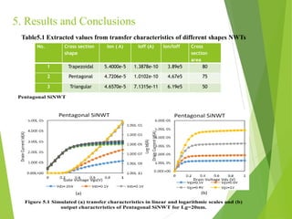
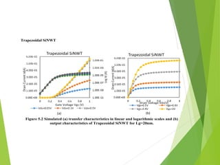
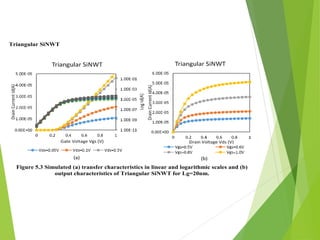
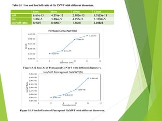
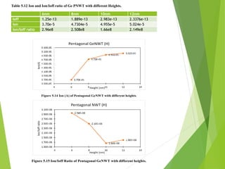
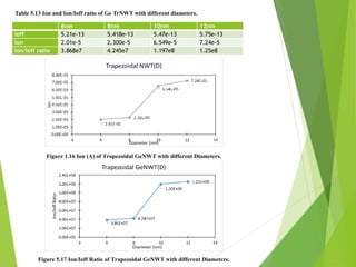
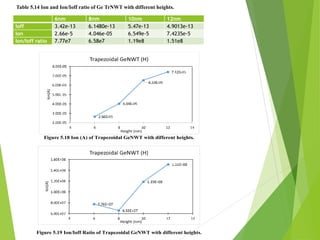


This document summarizes the design and performance analysis of 20nm silicon/germanium channel pentagonal and trapezoidal nanowire transistors. It presents the objectives of designing these nanowire transistors with different process parameters like diameter and height. The methodology involves using TCAD software to simulate the transfer characteristics, output characteristics, and short channel effects for different cross-sectional shapes and materials. The results show that pentagonal and trapezoidal nanowire transistors with germanium channels exhibit higher on-currents and on/off current ratios than triangular nanowire transistors. Key performance metrics like subthreshold swing and DIBL are also better for the pentagonal and trapezoidal nanowire transistors.


![Unit 4[1]](https://cdn.slidesharecdn.com/ss_thumbnails/unit41-120525191354-phpapp02-thumbnail.jpg?width=640&height=640&fit=bounds)


