____________________________________________________
______
PROJECT TITLE
INTRODUCTION TO DOUBLE GATE
MOSFET
SUBMITTED BY-
ADITYA KUMAR SINGH
AMRENDRA SHRIWASTAV
ABHISHEK KUMAR PATEL
UNDER THE GUIDANCE OF : Mrs. NEHA GOEL
1.Introduction to double gate
i. How can we follow Moore’s law
ii. Scaling
iii. Short channel effect
2.Literature Survey
3.Limitations of single gate MOSFET
4.Advantages of DG MOSFET
5.Refrences
The main idea of a Double Gate MOSFET is to control the Si channel
very efficiently by choosing the Si channel width to be very small and by
applying a gate contact to both sides of the channel. This concept helps
to suppress short channel effects and leads to higher currents as
compared with a MOSFET having only one gate.
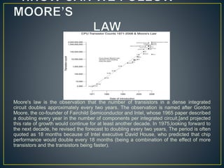
Moore's law is the observation that the number of transistors in a dense integrated
circuit doubles approximately every two years. The observation is named after Gordon
Moore, the co-founder of Fairchild Semiconductor and Intel, whose 1965 paper described
a doubling every year in the number of components per integrated circuit,[and projected
this rate of growth would continue for at least another decade. In 1975,looking forward to
the next decade, he revised the forecast to doubling every two years, The period is often
quoted as 18 months because of Intel executive David House, who predicted that chip
performance would double every 18 months (being a combination of the effect of more
transistors and the transistors being faster).
As aggressive scaling of conventional MOSFETs channel
length reduces below 100 nm and gate oxide thickness
below 3nm to improved performance and packing density.
Due to this scaling short channel effects (SCEs) like
threshold voltage roll-off & gate leakage current play a
major role in determining the performance of scaled
devices. The double gate (DG) MOSFETs are electro-
statically superior to a single gate (SG) MOSFET and
allows for additional gate length scaling
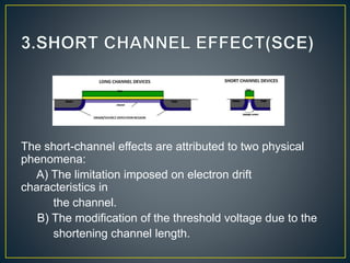
The short-channel effects are attributed to two physical
phenomena:
A) The limitation imposed on electron drift
characteristics in
the channel.
B) The modification of the threshold voltage due to the
shortening channel length.
Gerold W. Neudeck discussed the double gate (DG) fully
depleted SOI MOSFET ,and its many implementations, and
is the leading device candidate for silicon nano scale
CMOS. Their main characteristics, as compared to the
single gate bulk MOSFET are less S/D capacitance ,larger
saturated current drive, smaller short channel effects(DIBL)
, scalability to L=10nm ,near ideal sub threshold slopes (S)
,and the possibility of electrically adjustable threshold
voltages.
Ayushi Shrivastava and Nitin Tripathi compared 25nm
Single gate Silicon on Insulator (SG-SOI) MOSFET with
Double Gate Silicon on insulator(DG-SOI) MOSFET. The
DG-SOI is similar to the proposed SOI with the exception of
back gate at body. The resulted modified DG-SOI MOSFET
reduced the short channel effects (SCE’s) . The transfer
characteristics DIBL ,threshold voltage, Ion and Ioff for 25nm
are evaluated . The back gate structure of DG-SOI is the
mirror image of front gate SOI.
The nano scale device have SCEs ,like DIBL ,hot carried
effect , due to which the device can not be further scaled.
So ,this work is further demonstrated by designing two
gates on same dimension of single gate. So that, the DG-
SOI performance enhance and will work more efficiently.
• Limit for supply voltage
• Limit for further scaling of tox
• Minimum channel length Lg=100nm
• Dramatic short- channel effects (SCE)
• Short channel effect control
i. Better scalability
ii. Lower sub-threshold current
• Higher on current
• Lower gate leakage
• Elimination of Vt variation due to random dopant
fluctuation
1.Gerold W. Neudeck, “An Overview of Double-Gate
MOSFETs”, IEEE IN 47907-1285, July 2003
2.Ayushi Shrivastava , Nitin Tripathi, “Comparative study of
double gate MOSFET and single gate SOI
MOSFET”,IJEEE , Volume 07, Issue 01, Jan-June 2015
3.Xiaoping Liang ,“A 2-D Analytical Solution for SCEs in DG
MOSFETs”, VOL. 51, NO. 8, AUGUST 2004
THANK YOU

DOUBLE GATE MOSFET-BASICS

  • 1.
    ____________________________________________________ ______ PROJECT TITLE INTRODUCTION TODOUBLE GATE MOSFET SUBMITTED BY- ADITYA KUMAR SINGH AMRENDRA SHRIWASTAV ABHISHEK KUMAR PATEL UNDER THE GUIDANCE OF : Mrs. NEHA GOEL
  • 2.
    1.Introduction to doublegate i. How can we follow Moore’s law ii. Scaling iii. Short channel effect 2.Literature Survey 3.Limitations of single gate MOSFET 4.Advantages of DG MOSFET 5.Refrences
  • 3.
    The main ideaof a Double Gate MOSFET is to control the Si channel very efficiently by choosing the Si channel width to be very small and by applying a gate contact to both sides of the channel. This concept helps to suppress short channel effects and leads to higher currents as compared with a MOSFET having only one gate.
  • 4.
    Moore's law isthe observation that the number of transistors in a dense integrated circuit doubles approximately every two years. The observation is named after Gordon Moore, the co-founder of Fairchild Semiconductor and Intel, whose 1965 paper described a doubling every year in the number of components per integrated circuit,[and projected this rate of growth would continue for at least another decade. In 1975,looking forward to the next decade, he revised the forecast to doubling every two years, The period is often quoted as 18 months because of Intel executive David House, who predicted that chip performance would double every 18 months (being a combination of the effect of more transistors and the transistors being faster).
  • 5.
    As aggressive scalingof conventional MOSFETs channel length reduces below 100 nm and gate oxide thickness below 3nm to improved performance and packing density. Due to this scaling short channel effects (SCEs) like threshold voltage roll-off & gate leakage current play a major role in determining the performance of scaled devices. The double gate (DG) MOSFETs are electro- statically superior to a single gate (SG) MOSFET and allows for additional gate length scaling
  • 6.
    The short-channel effectsare attributed to two physical phenomena: A) The limitation imposed on electron drift characteristics in the channel. B) The modification of the threshold voltage due to the shortening channel length.
  • 7.
    Gerold W. Neudeckdiscussed the double gate (DG) fully depleted SOI MOSFET ,and its many implementations, and is the leading device candidate for silicon nano scale CMOS. Their main characteristics, as compared to the single gate bulk MOSFET are less S/D capacitance ,larger saturated current drive, smaller short channel effects(DIBL) , scalability to L=10nm ,near ideal sub threshold slopes (S) ,and the possibility of electrically adjustable threshold voltages.
  • 8.
    Ayushi Shrivastava andNitin Tripathi compared 25nm Single gate Silicon on Insulator (SG-SOI) MOSFET with Double Gate Silicon on insulator(DG-SOI) MOSFET. The DG-SOI is similar to the proposed SOI with the exception of back gate at body. The resulted modified DG-SOI MOSFET reduced the short channel effects (SCE’s) . The transfer characteristics DIBL ,threshold voltage, Ion and Ioff for 25nm are evaluated . The back gate structure of DG-SOI is the mirror image of front gate SOI. The nano scale device have SCEs ,like DIBL ,hot carried effect , due to which the device can not be further scaled. So ,this work is further demonstrated by designing two gates on same dimension of single gate. So that, the DG- SOI performance enhance and will work more efficiently.
  • 9.
    • Limit forsupply voltage • Limit for further scaling of tox • Minimum channel length Lg=100nm • Dramatic short- channel effects (SCE)
  • 10.
    • Short channeleffect control i. Better scalability ii. Lower sub-threshold current • Higher on current • Lower gate leakage • Elimination of Vt variation due to random dopant fluctuation
  • 11.
    1.Gerold W. Neudeck,“An Overview of Double-Gate MOSFETs”, IEEE IN 47907-1285, July 2003 2.Ayushi Shrivastava , Nitin Tripathi, “Comparative study of double gate MOSFET and single gate SOI MOSFET”,IJEEE , Volume 07, Issue 01, Jan-June 2015 3.Xiaoping Liang ,“A 2-D Analytical Solution for SCEs in DG MOSFETs”, VOL. 51, NO. 8, AUGUST 2004
  • 12.