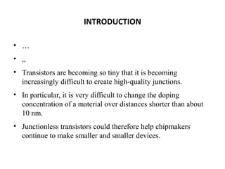
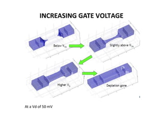
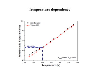
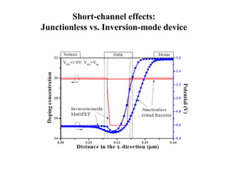
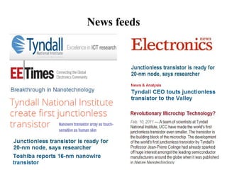
JUNCTIONLESS
TRANSISTOR
DIPU P
VIT University
dipugovind@gmail.com
News feeds @ a glance
INTRODUCTION
 All existing transistors junctions with junction are P–N junction
Heterojunction,Scotty junction,MOSFET, MESFET.
 The junctionless transistor (JLT) is a multigate FET with no PN nor N+N or
P+P junctions.
 The device is basically a resistor in which the mobile carrier density can
be modulated by the gate.
 Uniformly doped nanowire without junctions with a wrap-around gate.
 No junctions and no doping concentration gradients.
 They have near-ideal sub threshold slope,extremely low leakage currents,
and less degradation of mobility with gate voltage and temperature than
classical transistors.
INTRODUCTION
• …
• ,,
• Transistors are becoming so tiny that it is becoming
increasingly difficult to create high-quality junctions.
• In particular, it is very difficult to change the doping
concentration of a material over distances shorter than about
10 nm.
• Junctionless transistors could therefore help chipmakers
continue to make smaller and smaller devices.
STRUCTURE OF JUNCTIONLESS TRANSISTOR

Gated trans-resistor.
No junction.
Zero Doping concentration gradient.
Nano scale dimensions and high
FABRICATION PROCESS
Uniform Doping concentration.
Bulk conduction.
Beam lithography for nanowire and gates
For n-channeldevices
dopant: arsenic
channel concentration:
gate material: P+ polysilicon
INCREASING GATE VOLTAGE

At a Vd of 50 mV
INCREASING DRAIN VOLTAGE
Measured ID(VD) of N- and P-channel
junctionless transistors. L=1um, W=20nm
Measured ID(VG) of N- and P-channel
junctionless transistors. L=1um, W=20nm

ID, versus gate voltage, VG, for a drain voltage of +1 V in n-type and p-type
devices having a width of 30 nm and a length of 1 mm.
Temperature dependence
Short-channel effects:
Junctionless vs. Inversion-mode device
TYPES OF JUNCTIONLESS TRANSISTOR
 Junctionless MuGFET:
• This device has no junctions, a simpler fabrication process,
less variability and better electrical property than classical
inversion mode.
 Bulk Planar Junctionless Transistor (BPJLT):
• Highly scalable source–drain junction- free field-effect
transistor. It is thus junctionless in the source–channel–drain
path but needs a junction in the vertical direction for isolation
purposes
News feeds
Adv & Dis
• the lateral extension of the S/D depletion charges in the channel region
are causing short-channel effects such as DIBL and degraded
subthreshold slope. These are absent in a JLT
• Further improvement of the short-channel effects can be obtained by
increasing the extension of the gate control deeper in the source and
drain regions using high-κ spacers.
• one disadvantage of conventional junctionless transistors is that they
suffer from poor short-channel control.
• junctionless devices have the potential to operate at faster and use less
energy than the conventional transistors used in today's
microprocessors.
• They have near-ideal sub threshold
slope,extremely low leakage currents, and
less degradation of mobility with gate
voltage and temperature than classical
transistors.
CONCLUSION
 The devices have no junctions and are made in n+ or p+ silicon
nanowires.
 The devices have full CMOS functionality
 no junctions or doping gradients
 less sensitive to thermal budget issues than regular CMOS devices.
 a near-ideal subthreshold slope, close to60 mV/dec at room temperature
 extremely low leakage currents.
 Gated resistors exhibit less degradation of mobility than classical
transistors when the gate voltage is increased.
Reference
 Jean-Pierre ColingeTyndall National Institute, University College CorkLee Maltings, Cork, Ireland”
Junctionless Transistors” 978-1-4673-0836-6/12/$31.00 ©2012 IEEE
 Twinkal Solankia, Nilesh Parmar” A Review paper: A Comprehensive study of Junctionless
transistor”National Conference on Recent Trends in Engineering & Technology
 A. Kamath, Z. X. Chen, N. Shen, X. Li, N. Singh, G. Q. Lo, and D.-L. Kwong“Junctionless CMOS
Transistors with Independent Double Gates” International Journal of Information and Electronics
Engineering, Vol. 3, No. 1, January 2013.
 Baruch Feldman”Simulations of electronictransport in ultra-thin andultrashortjunctionlesstransistors”
 www.tyndall.ie
 http://www.tyndall.ie
 http://patents.justia.com/company/ibm

junctionless transistors

  • 1.
  • 2.
    News feeds @a glance
  • 3.
    INTRODUCTION  All existingtransistors junctions with junction are P–N junction Heterojunction,Scotty junction,MOSFET, MESFET.  The junctionless transistor (JLT) is a multigate FET with no PN nor N+N or P+P junctions.  The device is basically a resistor in which the mobile carrier density can be modulated by the gate.  Uniformly doped nanowire without junctions with a wrap-around gate.  No junctions and no doping concentration gradients.  They have near-ideal sub threshold slope,extremely low leakage currents, and less degradation of mobility with gate voltage and temperature than classical transistors.
  • 4.
    INTRODUCTION • … • ,, •Transistors are becoming so tiny that it is becoming increasingly difficult to create high-quality junctions. • In particular, it is very difficult to change the doping concentration of a material over distances shorter than about 10 nm. • Junctionless transistors could therefore help chipmakers continue to make smaller and smaller devices.
  • 5.
    STRUCTURE OF JUNCTIONLESSTRANSISTOR Gated trans-resistor. No junction. Zero Doping concentration gradient. Nano scale dimensions and high
  • 6.
    FABRICATION PROCESS Uniform Dopingconcentration. Bulk conduction. Beam lithography for nanowire and gates For n-channeldevices dopant: arsenic channel concentration: gate material: P+ polysilicon
  • 8.
  • 9.
  • 11.
    Measured ID(VD) ofN- and P-channel junctionless transistors. L=1um, W=20nm
  • 12.
    Measured ID(VG) ofN- and P-channel junctionless transistors. L=1um, W=20nm ID, versus gate voltage, VG, for a drain voltage of +1 V in n-type and p-type devices having a width of 30 nm and a length of 1 mm.
  • 13.
  • 14.
  • 15.
    TYPES OF JUNCTIONLESSTRANSISTOR  Junctionless MuGFET: • This device has no junctions, a simpler fabrication process, less variability and better electrical property than classical inversion mode.  Bulk Planar Junctionless Transistor (BPJLT): • Highly scalable source–drain junction- free field-effect transistor. It is thus junctionless in the source–channel–drain path but needs a junction in the vertical direction for isolation purposes
  • 16.
  • 17.
    Adv & Dis •the lateral extension of the S/D depletion charges in the channel region are causing short-channel effects such as DIBL and degraded subthreshold slope. These are absent in a JLT • Further improvement of the short-channel effects can be obtained by increasing the extension of the gate control deeper in the source and drain regions using high-κ spacers. • one disadvantage of conventional junctionless transistors is that they suffer from poor short-channel control. • junctionless devices have the potential to operate at faster and use less energy than the conventional transistors used in today's microprocessors.
  • 18.
    • They havenear-ideal sub threshold slope,extremely low leakage currents, and less degradation of mobility with gate voltage and temperature than classical transistors.
  • 19.
    CONCLUSION  The deviceshave no junctions and are made in n+ or p+ silicon nanowires.  The devices have full CMOS functionality  no junctions or doping gradients  less sensitive to thermal budget issues than regular CMOS devices.  a near-ideal subthreshold slope, close to60 mV/dec at room temperature  extremely low leakage currents.  Gated resistors exhibit less degradation of mobility than classical transistors when the gate voltage is increased.
  • 20.
    Reference  Jean-Pierre ColingeTyndallNational Institute, University College CorkLee Maltings, Cork, Ireland” Junctionless Transistors” 978-1-4673-0836-6/12/$31.00 ©2012 IEEE  Twinkal Solankia, Nilesh Parmar” A Review paper: A Comprehensive study of Junctionless transistor”National Conference on Recent Trends in Engineering & Technology  A. Kamath, Z. X. Chen, N. Shen, X. Li, N. Singh, G. Q. Lo, and D.-L. Kwong“Junctionless CMOS Transistors with Independent Double Gates” International Journal of Information and Electronics Engineering, Vol. 3, No. 1, January 2013.  Baruch Feldman”Simulations of electronictransport in ultra-thin andultrashortjunctionlesstransistors”  www.tyndall.ie  http://www.tyndall.ie  http://patents.justia.com/company/ibm

Editor's Notes