Download as PDF, PPTX


![Device design and simulation
µ1
µ2
[𝛴]1
Source Drain
Gate
𝑉𝐷𝑆
𝐼 𝐷𝑆
[𝛴]2
[H]
Green Function: 𝐺 = (𝐸𝐼 − 𝐻 − Σ 1 − Σ 2) −1
12
Abu Obayda EEE – 110 300 116](https://image.slidesharecdn.com/analyticalmodelingoftunnelingfieldeffecttransistortfet-170402163537/75/Analytical-Modeling-of-Tunneling-Field-Effect-Transistor-TFET-12-2048.jpg)
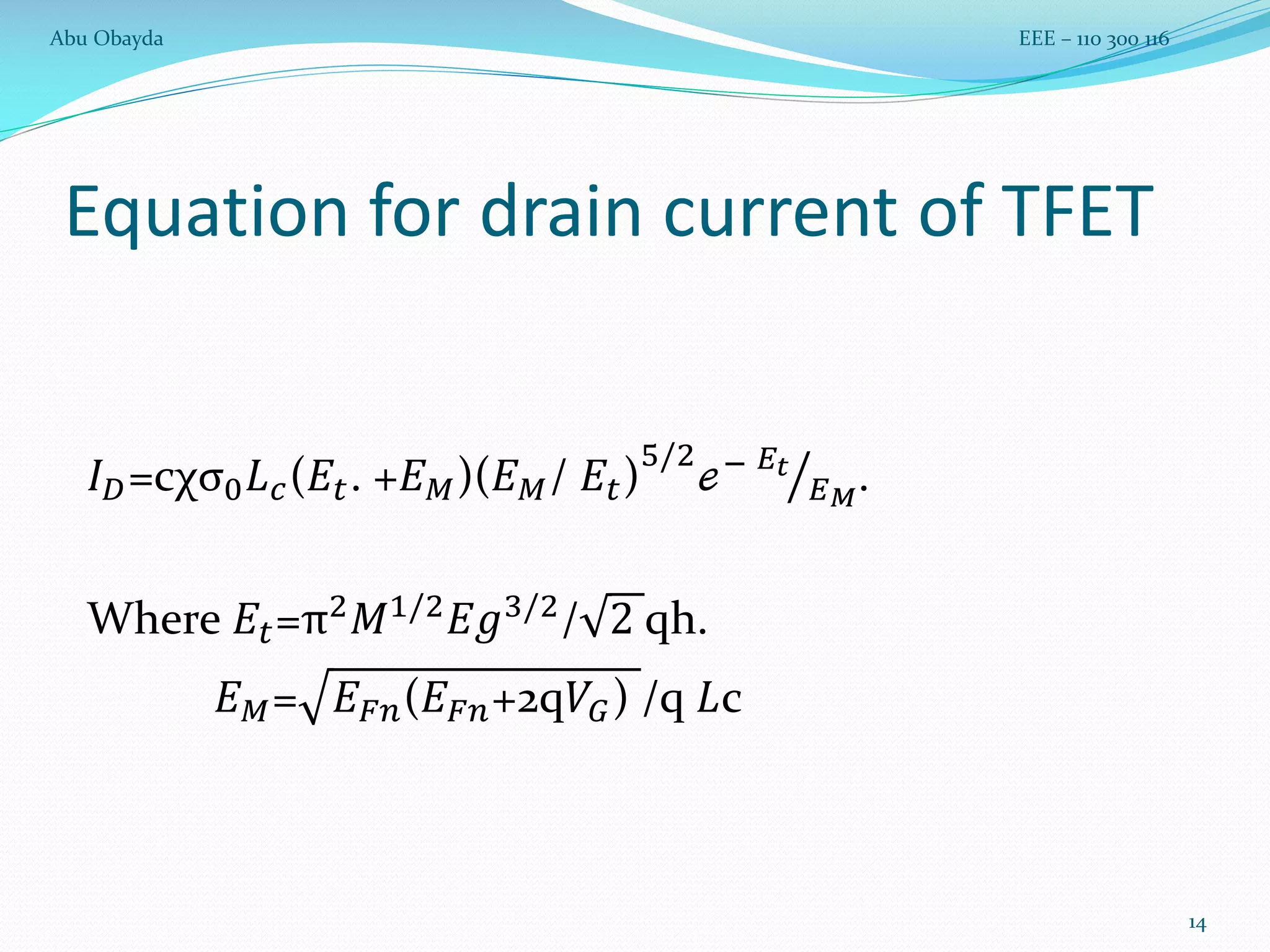
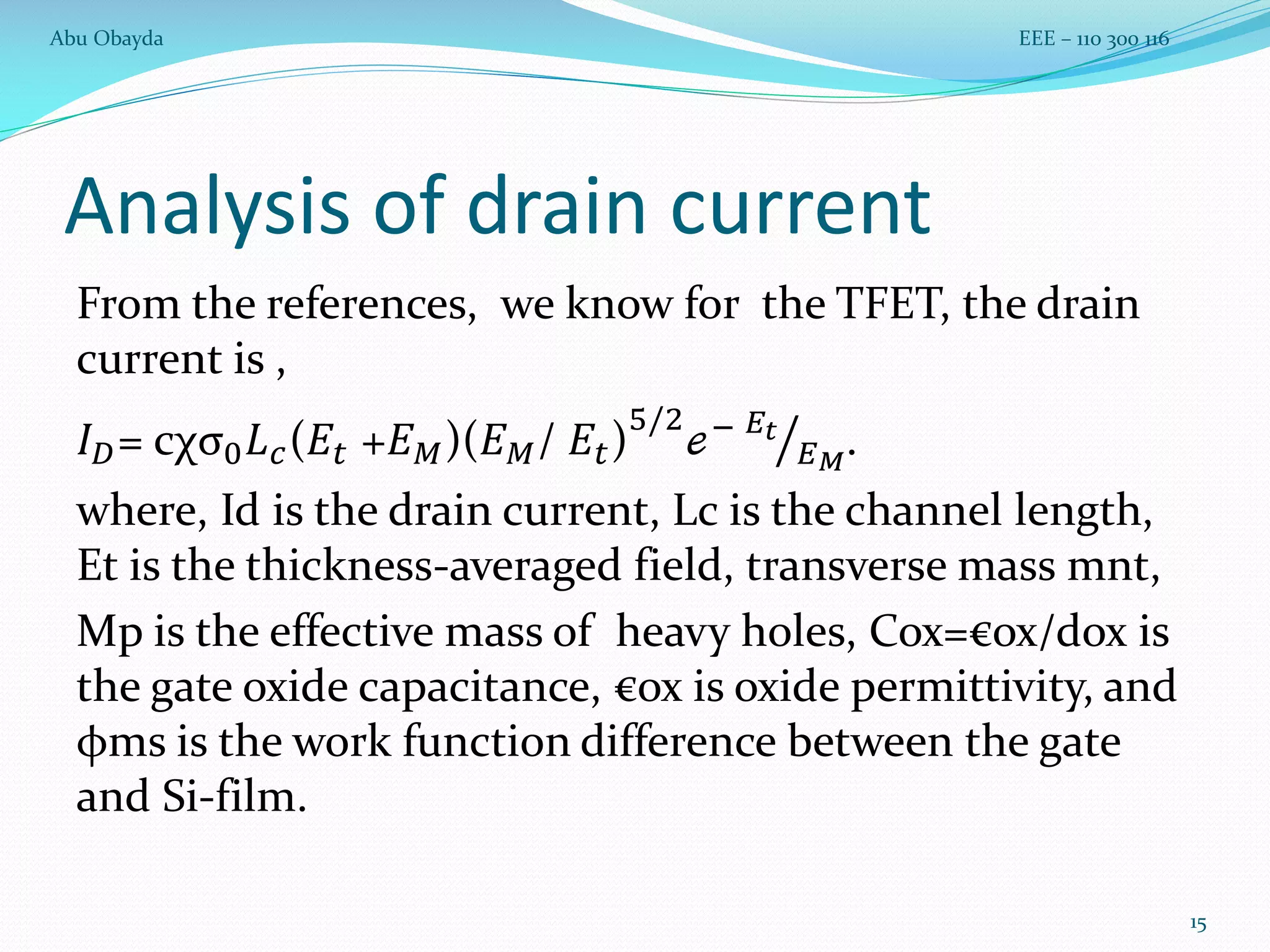
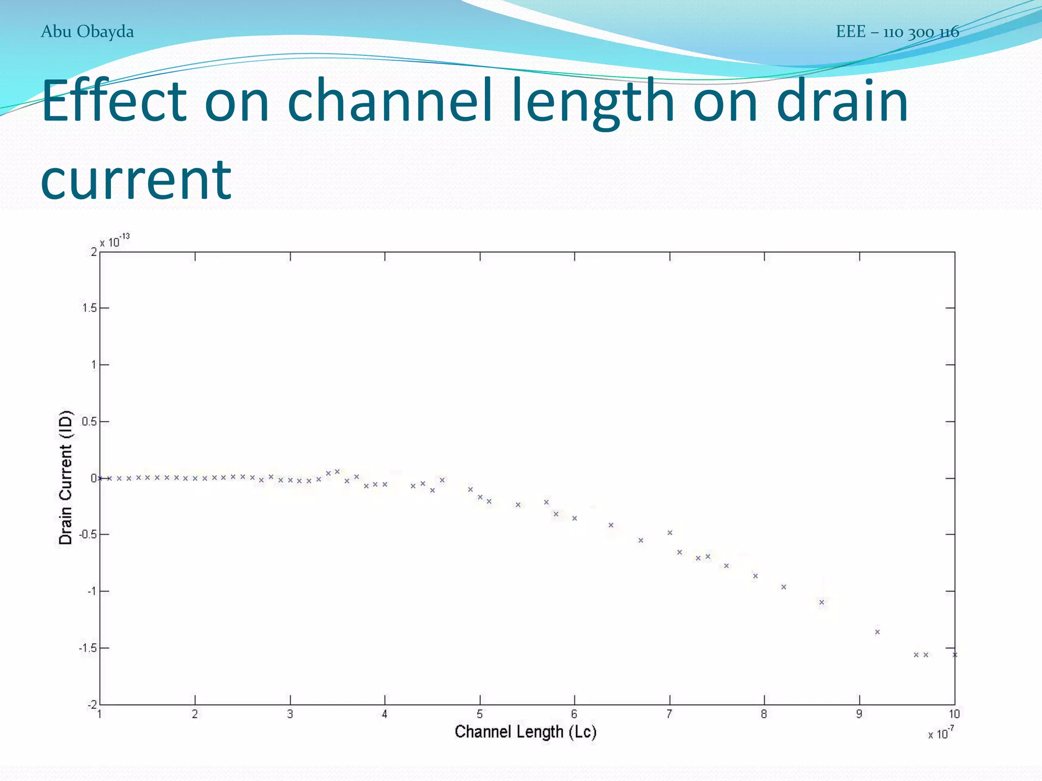
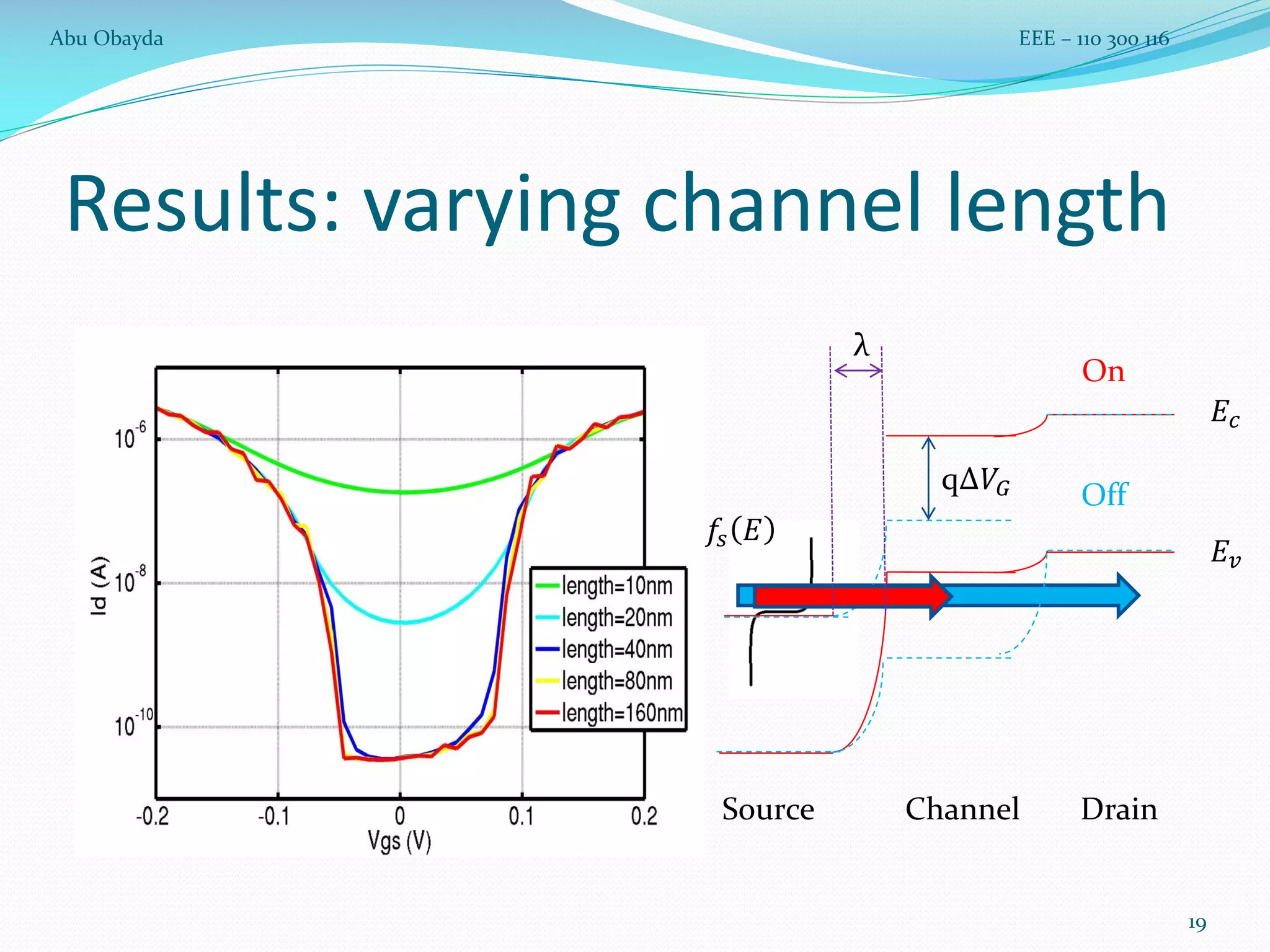

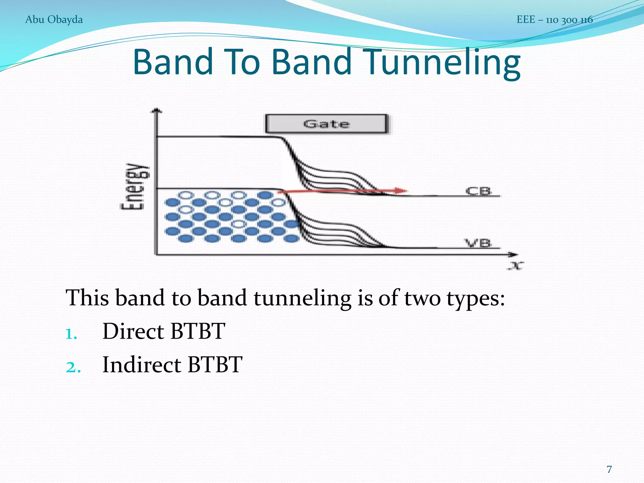
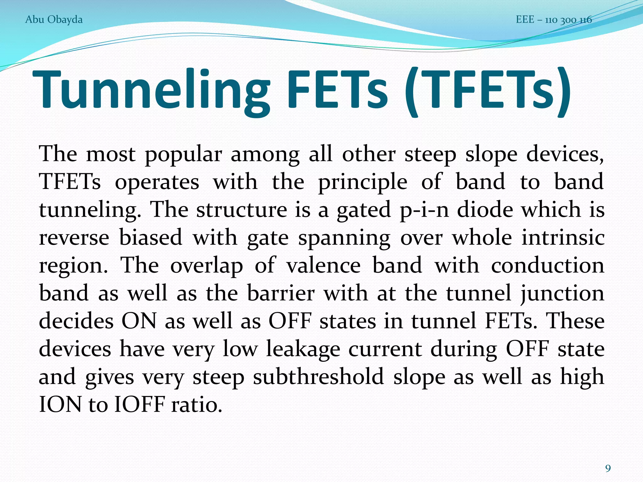
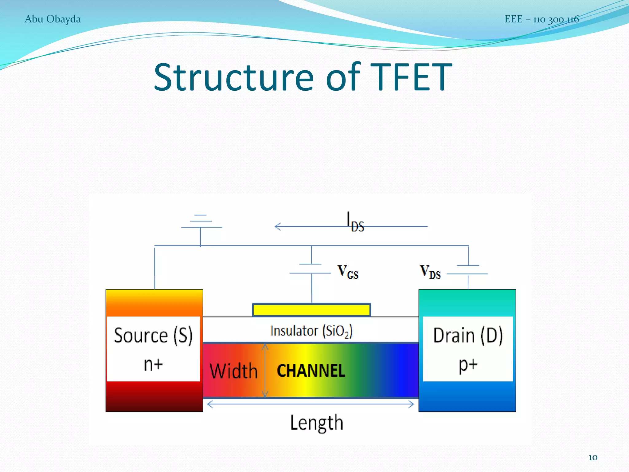
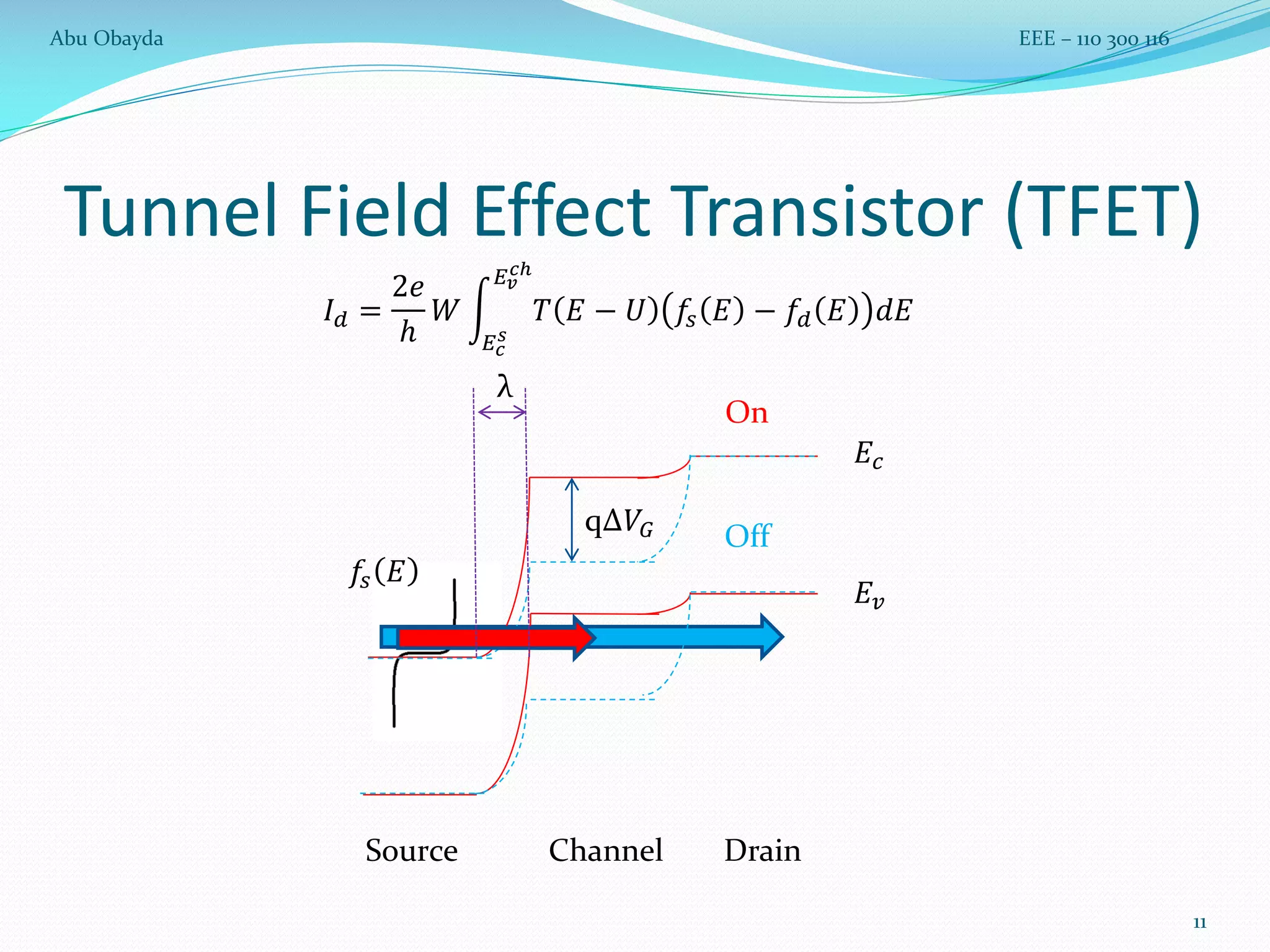
1. The document discusses the analytical modeling of tunnel field effect transistors (TFETs). TFETs are devices that can switch between on and off states at low voltages compared to MOSFETs. 2. TFETs operate using the principle of band-to-band tunneling, allowing for a steeper subthreshold slope than MOSFETs. However, TFETs currently have low drive currents that require further research to make them suitable for practical applications. 3. The document examines equations and parameters for calculating the drain current in TFETs and investigating the effects of channel length and gate voltage on this current. It also outlines some benefits and limitations of TFETs.