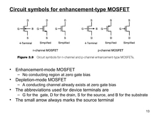
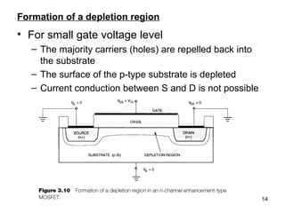
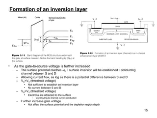
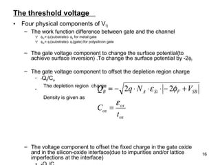
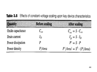
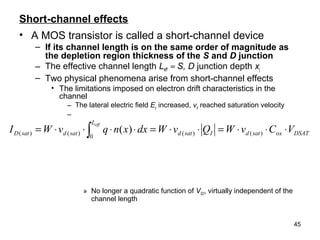
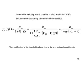
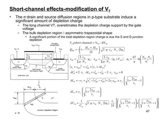
Downloaded 76 times

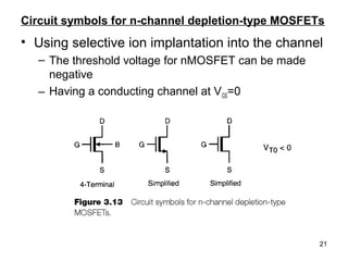
![26
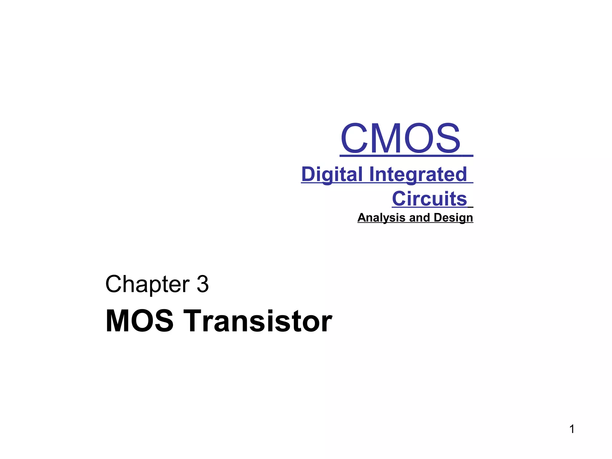
MOSFET current-voltage characteristics-gradual
channel approximation (GCA)(1)
• Considering linear mode operation
– VS=VB=0, the VGS and VDS are the external parameters controlling the drain current
ID
– VGS > VT0 (assume constant through the channel) to create a conducting inversion layer
– Defining
• X-direction: perpendicular to the surface, pointing down into the substrate
• Y-direction: parallel to the surface
– The y=0 is at the source end of the channel
– Channel voltage with respect to the source, Vc(y)
– Assume the electric field Ey is dominant compared with Ex
• This assumption reduced the current flow in the channel to the y-direction only
– Let QI(y) be the total mobile electron charge in the surface inversion layer
• QI(y)=-Cox[VGS-Vc(y)-VT0]](https://image.slidesharecdn.com/chapter3cmosclass2-130803112503-phpapp02/85/Chapter-3-cmos-class2-26-320.jpg)
![28
MOSFET current-voltage characteristics-gradual
channel approximation (GCA)(2)
( )
( )[ ]
( )[ ]
( )[ ] L
W
kwhere kVVVV
k
I
Cμwhere kVVVV
L
Wk
I
VVVV
L
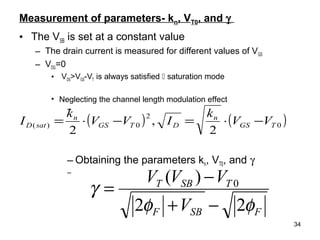
WC
I
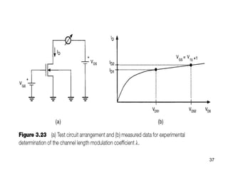
dVVVVCWLI
dVyQWdyI
dy
(y)QμW
I
-dRIdV
yisdropalongdThevoltage
μ
Q
(y)QμW
dy
dR
cesislincrementa
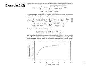
Theμ
'
DSDSTGSD
oxn
'
DSDSTGSD
DSDSTGS
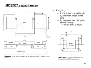
oxn
D
V
CTCGSoxnD
V
CI
L
D
In
D
DC
n
I
In
n
DS
DS
⋅=−−⋅⋅=
=−−⋅⋅⋅=
−−⋅⋅⋅
⋅
=
⋅−−⋅⋅=⋅
⋅⋅−=⋅
⋅
⋅⋅
=⋅=
⋅⋅
−=
∫
∫∫
2
0
2
0
'
2
0
0
0
0
n
0
2
2
2
2
2
2
)(
mobilityelectronbulktheofthatofhalf-oneabouttypicallyismagnitudeitsand
region,channeltheofionconcentratdopingon thedependentsmobilitysurfaceelectronThe
)chargelayerinversiontheofpolaritynegativethetodueissign(mimus
tanRe
mobilitysurfaceconstantahaslayerinversionin theelectronsmobileallthatAssumeing
µ
µ
µ](https://image.slidesharecdn.com/chapter3cmosclass2-130803112503-phpapp02/85/Chapter-3-cmos-class2-28-320.jpg)
![30
MOSFET current-voltage characteristics-gradual
channel approximation (GCA)-saturation region
• For VDS≥VDSAT=VGS-VT0
–
– The drain current becomes a function only of VGS, beyond the saturation boundary
( ) ( ) ( )[ ]
( )2
0
2
000)(
2
2
2
TGS
oxn
TGSTGSTGS
oxn
satD
VV
L
WC
VVVVVV
L
WC
I
−⋅⋅
⋅
=
−−−⋅−⋅⋅⋅
⋅
=
µ
µ](https://image.slidesharecdn.com/chapter3cmosclass2-130803112503-phpapp02/85/Chapter-3-cmos-class2-30-320.jpg)
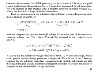
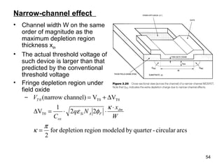
![32
Substrate bias effect
• The discussion in the previous has been done under the assumption
– The substrate potential is equal to the source potential, i.e. VSB=0
• On the other hand
– the source potential of an nMOS transistor can be larger than the substrate
potential, i.e. VSB>0
– ( )
( )[ ]
( ) ( )DSSBTGS
oxn
satD
DSDSSBTGS
oxn
linD
FSBFTSBT
VVVV
L
WC
I
VVVVV
L
WC
I
VVVV
⋅+⋅−⋅⋅
⋅
=
−−⋅⋅⋅
⋅
=
−+⋅+=
λ
µ
µ
φφγ
1)(
2
)(2
2
22)(
2
)(
2
)(
0](https://image.slidesharecdn.com/chapter3cmosclass2-130803112503-phpapp02/85/Chapter-3-cmos-class2-32-320.jpg)
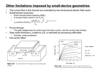
![33
Current-voltage equation of n-, p-channel MOSFET
( )[ ]
( ) ( )
( )[ ]
( ) ( )
TGSDS
TGSDSTGS
oxp
satD
TGSDS
TGSDSDSTGS
oxp
linD
TGSD
TGSDS
TGSDSTGS
oxn
satD
TGSDS
TGSDSDSTGS
oxn
linD
TGSD
-VVV
VVVVV
L
WC
I
-VVV
VVVVVV
L
WC
I
VVI
-VVV
VVVVV
L
WC
I
-VVV
VVVVVV
L
WC
I
VVI
≤
≤⋅+⋅−⋅⋅
⋅
=
>
≤−−⋅⋅⋅
⋅
=
>=
≥
≥⋅+⋅−⋅⋅
⋅
=
<
≥−−⋅⋅⋅
⋅
=
<=
and
for1
2
and
for2
2
for,0
MOSFETchannel-pFor
and
for1
2
and
for2
2
for,0
MOSFETchannel-nFor
2
)(
2
)(
2
)(
2
)(
λ
µ
µ
λ
µ
µ](https://image.slidesharecdn.com/chapter3cmosclass2-130803112503-phpapp02/85/Chapter-3-cmos-class2-33-320.jpg)
![40
Full scaling (constant-field scaling)
( )[ ]
( )[ ]
( ) ( )
sresistanceabdescapacitancparasiticvariousofreductionA
improveddown time-chargeandup,-chargetheoffactorabydownscaledis
unchangedvirtuallyremainingareaunitperThe
scalingfulloffeaturesattractivemosttheofoneisndissipatiopowertheofreductiontsignificanThe
1
ndissipatiopowerThe
1
22
currentdrainmodesaturationThe
2
1
2
2
2
currentdrainmodelinearThe
offactorabyscaledalsowilltheunchangedratioaspectThe
C
areaunitperecapacitancoxidegateThe
densitydopingscaledby theaffectedtlysignificannotismobilitysurfacetheAssuming
factorscalingsameby theally,proportiondownscaledbemustpotentialsallgoal,thisachieveTo
22
2
2
2
2
2
2
'
'
ox
⇒
=⋅⋅=⋅=
=−⋅⋅
⋅
=−⋅=
=−⋅−⋅⋅⋅
⋅
=
−⋅−⋅⋅=
⇒
⋅=⋅==
SC
itypower dens
S
P
VI
S
VIP
S
I
VV
S
kS
VV
k
(sat)I
S
I
VVVV
S
kS
VVVV
k
(lin)I
SkW/L
CS
t
S
t
μ
g
DSD
'
DS
'
D
'
D(sat)
TGS
n'
T
'
GS
'
n'
D
D(lin)
DSDSTGS
n
'
DS
'
DS
'
T
'
GS
'
n'
D
n
ox
ox
ox
ox
ox
n
εε](https://image.slidesharecdn.com/chapter3cmosclass2-130803112503-phpapp02/85/Chapter-3-cmos-class2-40-320.jpg)
![43
Constant-voltage scaling
( )[ ]
( )[ ]
( ) ( )
stress-overelectricalandbreakdown,oxiden,degradatiocarrierhotration,electromig
densitypowerdensity,currentincreasingDisadv.
s.constraintlevel-voltageexternaltheofbecause
casespracticalmamyinscalingfulloverpreferredbemayscalingvoltage-constant,summarizedTo
offactorabyincresaeddensitypowerThe
ndissipatiopowerThe
offactorabyincreaseddensitycurrentdrainThe
22
currentdrainmodesaturationThe
2
2
2
2
currentdrainmodelinearThe
byincreasedalsoisparameteructancetranscondThe
offactorabyincreasedisareaunitperecapacitancoxidegateThe
relationsfield-chargethepreserveorder toinoffactorabyincreasedbemustdensitiesdopingThe
unchanged.remainedvoltagesterminaltheandtagesupply volpowerThe
.offactorabyreducedMOSFETaretheofdimensionsAll
3
3
22
2
2
2
⇒
⇒
⋅=⋅⋅=⋅=
⋅=−⋅
⋅
=−=
⋅=−⋅−⋅⋅
⋅
=
−⋅−⋅⋅=
⇒
S
PSV)I(SVIP
S
(sat)ISVV
kS
VV
k
(sat)I
(lin)ISVVVV
kS
VVVV
k
(lin)I
S
SC
S
S
DSD
'
DS
'
D
'
DTGS
n'
T
'
GS
'
n'
D
DDSDSTGS
n
'
DS
'
DS
'
T
'
GS
'
n'
D
ox](https://image.slidesharecdn.com/chapter3cmosclass2-130803112503-phpapp02/85/Chapter-3-cmos-class2-43-320.jpg)

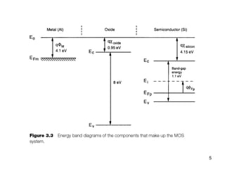
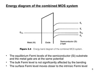
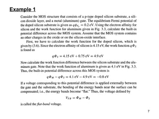
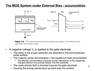
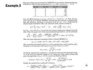
The document discusses the MOS transistor structure and its operation. It begins by describing the basic MOS structure consisting of a metal gate, oxide layer, and semiconductor substrate. It then explains the energy band diagrams and how applying different gate biases can cause accumulation, depletion, or inversion at the surface. The document also covers MOSFET operation in different regions, the gradual channel approximation used to derive current equations, threshold voltage, channel length modulation, and the effect of substrate bias.


