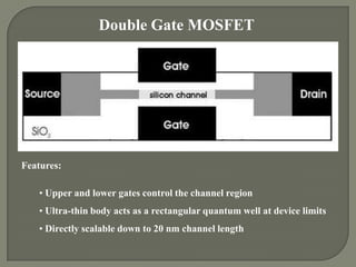
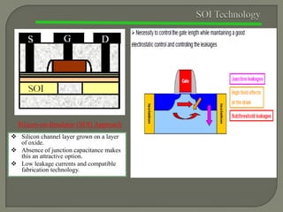
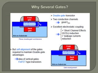
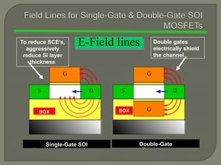
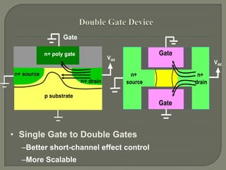
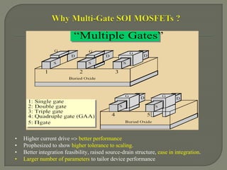
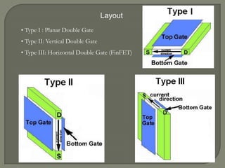
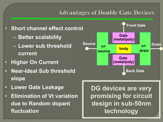
SlideShare a Scribd company logo
DOUBLE - GATE MOSFET

BY,
A. POOJA SHUKLA
1821310006
M. Tech ( I Yr )
SRM UNIVERSITY
A BASIC MOSFET:
MOSFET Transistor Fabrication Steps
MOSFET OPERATION
Step 1: Apply Gate Voltage
SiO2 Insulator (Glass)
Gate

Source

Drain
5 volts

holes

N

N

electrons
P
electrons to be
transmitted
Step 2: Excess electrons surface
in channel, holes are repelled.

Step 3: Channel becomes
saturated with electrons.
Electrons in source are able to
flow across channel to Drain.
Scaling limits of BULK MOSFET

 Limit

for supply voltage (<0.6V)

 Limit

for further scaling of tox (<2nm)

 Minimum

 Discrete

channel length Lg=50nm

dopant fluctuations

 Dramatic

short-channels effects (SCE)
Problem 1: Carrier Mobility Decreases as Channel

length decrease and Vertical Electric fields increase
Problem 2: VT Rolloff as Channel length decreases
Problem 3: Tunneling Through Gate Oxide (off state
current)
Problem 4: Wattage/Area increases as density increases
How can we follow Moore’s law ?
 By moving to DG MOSFETs
DG might be the unique viable alternative to build nano
MOSFETs when Lg<50nm
Because:
- Better control of the channel from the gates
- Reduced short-channel effects
- Better Ion/Ioff

- Improved sub-threshold slope (60mV/decade)
- No discrete dopant fluctuations
Double Gate MOSFET

Features:
• Upper and lower gates control the channel region
• Ultra-thin body acts as a rectangular quantum well at device limits
• Directly scalable down to 20 nm channel length
Silicon-on-Insulator (SOI) Approach
 Silicon channel layer grown on a layer
of oxide.
 Absence of junction capacitance makes
this an attractive option.
 Low leakage currents and compatible
fabrication technology.
Silicon-on-Insulator (SOI) Approach
 Silicon channel layer grown on a layer
of oxide.
 Absence of junction capacitance makes
this an attractive option.
 Low leakage currents and compatible
fabrication technology.
To reduce SCE’s,
aggressively
reduce Si layer
thickness

E-Field lines

G
S

BOX

Double gates
electrically shield
the channel

G
D

S

BOX

D
G

Double-Gate
Regular SOI MOSFET Double-gate MOSFET
Single-Gate SOI
Gate
n+ poly gate

Gate

Vdd

n+ source
n+ drain

Vdd
n+
source

n+
drain

p substrate

Gate

• Single Gate to Double Gates
–Better short-channel effect control
–More Scalable
•
•
•
•

Higher current drive
better performance
Prophesized to show higher tolerance to scaling.
Better integration feasibility, raised source-drain structure, ease in integration.
Larger number of parameters to tailor device performance
Layout
• Type I : Planar Double Gate
• Type II: Vertical Double Gate
• Type III: Horizontal Double Gate (FinFET)
Reduced Channel and Gate Leakage

• Short channel effects are seen in Standard silicon MOS devices
• DGFET offers greater control of the channel because of the double gate
• Gate leakage current is prevented by a thick gate oxide
Threshold Voltage Control

Silicon MOS Transistor:
• Increased body doping used to control VT for short channel
• Small number of dopant atoms for very short channel
• Lowest VT achievable is .5V

Double Gate FET :
• Increased body doping
• Asymmetric gate work functions (n+ / p+ gates)

• Metal gate
• VT of .1V achievable through work function engineering
Increased Carrier Mobility

Silicon MOS Transistor:
• Carrier scattering from increased body doping
• Transverse electric fields from the source and drain reduce mobility

Double Gate FET:
• Lightly doped channel in a DGFET results in a negligible depletion charge
• Asymmetric gate: experiences some transverse electric fields

• Metal gate: transverse electric field negligible with increased channel control
Reduced Power Consumption
• Double Gate coupling allows for higher drive currents at lower supply
voltage and threshold voltage
• Energy is a quadratic function of supply voltage

• Reduced channel and gate leakage currents in off state translate to huge
power savings
• Separate control of each gate allows dynamic control of VT :
Simplified logic gates would save power and chip area
Challenges Facing Double Gate Technology
1) Identically sized gates
2) Self-alignment of source and drain to both gates
3) Alignment of both gates to each other
4) Connecting two gates with a low-resistance path
Ultimate Double Gate Limits
1) Thermionic emission above the channel potential barrier:
Short channel effects lower potential barrier

2) Band-to-band tunneling between body and drain pn junction:
Body-drain electric field increases tunneling probability
3) Quantum mechanical tunneling directly between source and drain:
Extremely small channel lengths correspond to narrow
potential barrier width
4) Other effects of quantum confinement in the thin body
Front Gate

• Short channel effect control
– Better scalability
– Lower sub threshold
current
• Higher On Current

• Near-Ideal Sub threshold
slope
• Lower Gate Leakage

• Elimination of Vt variation
due to Random dopant
fluctuation

Gate
(metal/poly)
Source

n+
source

body

Drain
n+
drain

Gate
(metal/poly)
Back Gate

DG devices are very
promising for circuit
design in sub-50nm
technology
THANK YOU…….!!!

More Related Content

What's hot

Finfet
FinfetFinfet
Finfet
Aditya Singh
 
Finfet Technology
Finfet TechnologyFinfet Technology
Finfet Technology
Srinivas Vasamsetti
 
3673 mosfet
3673 mosfet3673 mosfet
3673 mosfet
vidhya DS
 
CMOS
CMOS CMOS
MOS Capacitor
MOS CapacitorMOS Capacitor
Silicon on Insulator (SOI) Technology
Silicon on Insulator (SOI) TechnologySilicon on Insulator (SOI) Technology
Silicon on Insulator (SOI) Technology
Sudhanshu Janwadkar
 
Device isolation Techniques
Device isolation TechniquesDevice isolation Techniques
Device isolation Techniques
Sudhanshu Janwadkar
 
C-V characteristics of MOS Capacitor
C-V characteristics of MOS CapacitorC-V characteristics of MOS Capacitor
C-V characteristics of MOS Capacitor
RCC Institute of Information Technology
 
Short channel effects
Short channel effectsShort channel effects
Short channel effects
Esmaeil Javadi
 
High k dielectrics
High k dielectricsHigh k dielectrics
High k dielectricsSubash John
 
MOSFET, SOI-FET and FIN-FET-ABU SYED KUET
MOSFET, SOI-FET and FIN-FET-ABU SYED KUETMOSFET, SOI-FET and FIN-FET-ABU SYED KUET
MOSFET, SOI-FET and FIN-FET-ABU SYED KUETA. S. M. Jannatul Islam
 
Introduction to FinFET
Introduction to FinFETIntroduction to FinFET
Introduction to FinFET
ManishKenchi
 
LOW POWER DESIGN VLSI
LOW POWER DESIGN VLSILOW POWER DESIGN VLSI
LOW POWER DESIGN VLSI
Duronto riyad
 
Second order effects
Second order effectsSecond order effects
Second order effects
PRAVEEN KUMAR CHITLURI
 
Ic tech unit 5- VLSI Process Integration
Ic tech unit 5- VLSI Process IntegrationIc tech unit 5- VLSI Process Integration
Ic tech unit 5- VLSI Process Integration
kriticka sharma
 
Presentation on Scaling
Presentation on ScalingPresentation on Scaling
Presentation on Scaling
Raviraj Kaur
 
MOSFETs
MOSFETsMOSFETs
MOSFETs
A B Shinde
 
Fully depleted silicon insulator
Fully depleted silicon insulatorFully depleted silicon insulator
Fully depleted silicon insulator
sandeep sandy
 
Short-Channel Effects in MOSFET
Short-Channel Effects in MOSFETShort-Channel Effects in MOSFET
Short-Channel Effects in MOSFET
RCC Institute of Information Technology
 

What's hot (20)

Finfet
FinfetFinfet
Finfet
 
Finfet Technology
Finfet TechnologyFinfet Technology
Finfet Technology
 
3673 mosfet
3673 mosfet3673 mosfet
3673 mosfet
 
CMOS
CMOS CMOS
CMOS
 
MOS Capacitor
MOS CapacitorMOS Capacitor
MOS Capacitor
 
Silicon on Insulator (SOI) Technology
Silicon on Insulator (SOI) TechnologySilicon on Insulator (SOI) Technology
Silicon on Insulator (SOI) Technology
 
Device isolation Techniques
Device isolation TechniquesDevice isolation Techniques
Device isolation Techniques
 
C-V characteristics of MOS Capacitor
C-V characteristics of MOS CapacitorC-V characteristics of MOS Capacitor
C-V characteristics of MOS Capacitor
 
Short channel effects
Short channel effectsShort channel effects
Short channel effects
 
High k dielectrics
High k dielectricsHigh k dielectrics
High k dielectrics
 
MOSFET, SOI-FET and FIN-FET-ABU SYED KUET
MOSFET, SOI-FET and FIN-FET-ABU SYED KUETMOSFET, SOI-FET and FIN-FET-ABU SYED KUET
MOSFET, SOI-FET and FIN-FET-ABU SYED KUET
 
Introduction to FinFET
Introduction to FinFETIntroduction to FinFET
Introduction to FinFET
 
LOW POWER DESIGN VLSI
LOW POWER DESIGN VLSILOW POWER DESIGN VLSI
LOW POWER DESIGN VLSI
 
Second order effects
Second order effectsSecond order effects
Second order effects
 
Ic tech unit 5- VLSI Process Integration
Ic tech unit 5- VLSI Process IntegrationIc tech unit 5- VLSI Process Integration
Ic tech unit 5- VLSI Process Integration
 
Presentation on Scaling
Presentation on ScalingPresentation on Scaling
Presentation on Scaling
 
MOSFETs
MOSFETsMOSFETs
MOSFETs
 
Fully depleted silicon insulator
Fully depleted silicon insulatorFully depleted silicon insulator
Fully depleted silicon insulator
 
Latch up
Latch upLatch up
Latch up
 
Short-Channel Effects in MOSFET
Short-Channel Effects in MOSFETShort-Channel Effects in MOSFET
Short-Channel Effects in MOSFET
 

Viewers also liked

Finfet; My 3rd PPT in clg
Finfet; My 3rd PPT in clgFinfet; My 3rd PPT in clg
Finfet; My 3rd PPT in clgARUNASUJITHA
 
Fin Fet Technology by SAMRA
Fin Fet  Technology by SAMRAFin Fet  Technology by SAMRA
Fin Fet Technology by SAMRA
Bal Partap Singh
 
finfet & dg-fet technology
finfet & dg-fet technologyfinfet & dg-fet technology
finfet & dg-fet technology
Kritika Ramesh
 
Mosfet
MosfetMosfet
Mosfet
Pooja Shukla
 
junctionless transistors
junctionless transistorsjunctionless transistors
junctionless transistorsdipugovind
 
oral defense_07212012
oral defense_07212012oral defense_07212012
oral defense_07212012YU-CHUN YIN
 
Double Patterning
Double PatterningDouble Patterning
Double PatterningDanny Luk
 
Fabrication of silicon on insulator (soi)
Fabrication of silicon on insulator (soi)Fabrication of silicon on insulator (soi)
Fabrication of silicon on insulator (soi)Pooja Shukla
 
Double patterning for 32nm and beyond
Double patterning for 32nm and beyondDouble patterning for 32nm and beyond
Double patterning for 32nm and beyond
Manikandan Sampathkumar
 
3D or Tri-gate transistors
3D or Tri-gate transistors3D or Tri-gate transistors
3D or Tri-gate transistors
Karanvir Singh
 
Ultra-thin body SOI MOSFETs: Term Paper_class presentation on Advanced topics...
Ultra-thin body SOI MOSFETs: Term Paper_class presentation on Advanced topics...Ultra-thin body SOI MOSFETs: Term Paper_class presentation on Advanced topics...
Ultra-thin body SOI MOSFETs: Term Paper_class presentation on Advanced topics...
prajon
 
Flipflop
FlipflopFlipflop
Flipflop
sohamdodia27
 
CMOS logic circuits
CMOS logic circuitsCMOS logic circuits
CMOS logic circuits
Mahesh_Naidu
 
Mosfet
MosfetMosfet
Analysis Of 3C-Sic Double Implanted MOSFET With Gaussian Profile Doping In Th...
Analysis Of 3C-Sic Double Implanted MOSFET With Gaussian Profile Doping In Th...Analysis Of 3C-Sic Double Implanted MOSFET With Gaussian Profile Doping In Th...
Analysis Of 3C-Sic Double Implanted MOSFET With Gaussian Profile Doping In Th...
IJRES Journal
 

Viewers also liked (20)

Finfet; My 3rd PPT in clg
Finfet; My 3rd PPT in clgFinfet; My 3rd PPT in clg
Finfet; My 3rd PPT in clg
 
Fin Fet Technology by SAMRA
Fin Fet  Technology by SAMRAFin Fet  Technology by SAMRA
Fin Fet Technology by SAMRA
 
finfet & dg-fet technology
finfet & dg-fet technologyfinfet & dg-fet technology
finfet & dg-fet technology
 
Mosfet
MosfetMosfet
Mosfet
 
junctionless transistors
junctionless transistorsjunctionless transistors
junctionless transistors
 
oral defense_07212012
oral defense_07212012oral defense_07212012
oral defense_07212012
 
Double Patterning
Double PatterningDouble Patterning
Double Patterning
 
Fabrication of silicon on insulator (soi)
Fabrication of silicon on insulator (soi)Fabrication of silicon on insulator (soi)
Fabrication of silicon on insulator (soi)
 
Double patterning for 32nm and beyond
Double patterning for 32nm and beyondDouble patterning for 32nm and beyond
Double patterning for 32nm and beyond
 
3D or Tri-gate transistors
3D or Tri-gate transistors3D or Tri-gate transistors
3D or Tri-gate transistors
 
Ultra-thin body SOI MOSFETs: Term Paper_class presentation on Advanced topics...
Ultra-thin body SOI MOSFETs: Term Paper_class presentation on Advanced topics...Ultra-thin body SOI MOSFETs: Term Paper_class presentation on Advanced topics...
Ultra-thin body SOI MOSFETs: Term Paper_class presentation on Advanced topics...
 
SOI
SOISOI
SOI
 
Flipflop
FlipflopFlipflop
Flipflop
 
CMOS logic circuits
CMOS logic circuitsCMOS logic circuits
CMOS logic circuits
 
P1121110526
P1121110526P1121110526
P1121110526
 
digital
digitaldigital
digital
 
n-MOS Fabrication Process
n-MOS Fabrication Processn-MOS Fabrication Process
n-MOS Fabrication Process
 
Mosfet
MosfetMosfet
Mosfet
 
Slideshare ppt
Slideshare pptSlideshare ppt
Slideshare ppt
 
Analysis Of 3C-Sic Double Implanted MOSFET With Gaussian Profile Doping In Th...
Analysis Of 3C-Sic Double Implanted MOSFET With Gaussian Profile Doping In Th...Analysis Of 3C-Sic Double Implanted MOSFET With Gaussian Profile Doping In Th...
Analysis Of 3C-Sic Double Implanted MOSFET With Gaussian Profile Doping In Th...
 

Similar to Double gate mosfet

Advanced mosfet architectures
Advanced mosfet architecturesAdvanced mosfet architectures
Advanced mosfet architectures
Denita Tom
 
Mosfet ppt by dhwani sametriya
Mosfet ppt by dhwani sametriyaMosfet ppt by dhwani sametriya
Mosfet ppt by dhwani sametriya
Dhwani Sametriya
 
mosfet scaling_
mosfet scaling_mosfet scaling_
mosfet scaling_
Web Design & Development
 
Structural and Electrical Analysis of Various MOSFET Designs
Structural and Electrical Analysis of Various MOSFET DesignsStructural and Electrical Analysis of Various MOSFET Designs
Structural and Electrical Analysis of Various MOSFET Designs
IJERA Editor
 
Rosh ppt
Rosh pptRosh ppt
Rosh ppt
Rosh Mani
 
Dual Metal Gate and Conventional MOSFET at Sub nm for Analog Application
Dual Metal Gate and Conventional MOSFET at Sub nm for Analog ApplicationDual Metal Gate and Conventional MOSFET at Sub nm for Analog Application
Dual Metal Gate and Conventional MOSFET at Sub nm for Analog Application
VLSICS Design
 
tri gate transistors
tri gate transistorstri gate transistors
tri gate transistors
Chetan Kataria
 
Carbon nanotube based Field Effect Transistor
Carbon nanotube based Field Effect TransistorCarbon nanotube based Field Effect Transistor
Carbon nanotube based Field Effect Transistor
Sushmita Dandeliya
 
small geometry effect and working of solar cell
small geometry effect and working of solar cellsmall geometry effect and working of solar cell
small geometry effect and working of solar cell
Shivank Rastogi
 
Nano devices- resonant tunneling diode, resonant tunneling transistor, SET, F...
Nano devices- resonant tunneling diode, resonant tunneling transistor, SET, F...Nano devices- resonant tunneling diode, resonant tunneling transistor, SET, F...
Nano devices- resonant tunneling diode, resonant tunneling transistor, SET, F...
pondicherry university
 
A Study On Double Gate Field Effect Transistor For Area And Cost Efficiency
A Study On Double Gate Field Effect Transistor For Area And Cost EfficiencyA Study On Double Gate Field Effect Transistor For Area And Cost Efficiency
A Study On Double Gate Field Effect Transistor For Area And Cost Efficiency
paperpublications3
 
20EC602 VLSI Design.ppt
20EC602 VLSI Design.ppt20EC602 VLSI Design.ppt
20EC602 VLSI Design.ppt
ASureshkumar13
 
ULTRA HIGH SPEED FACTORIAL DESIGN IN SUB-NANOMETER TECHNOLOGY
ULTRA HIGH SPEED FACTORIAL DESIGN IN SUB-NANOMETER TECHNOLOGYULTRA HIGH SPEED FACTORIAL DESIGN IN SUB-NANOMETER TECHNOLOGY
ULTRA HIGH SPEED FACTORIAL DESIGN IN SUB-NANOMETER TECHNOLOGY
cscpconf
 
Introduction gadgets have gained a lot of attention.pdf
Introduction gadgets have gained a lot of attention.pdfIntroduction gadgets have gained a lot of attention.pdf
Introduction gadgets have gained a lot of attention.pdf
bkbk37
 
Metal Insulator Semiconductor devices
Metal Insulator Semiconductor devicesMetal Insulator Semiconductor devices
Metal Insulator Semiconductor devices
utpal sarkar
 
A NOVEL POWER REDUCTION TECHNIQUE FOR DUAL-THRESHOLD DOMINO LOGIC IN SUB-65NM...
A NOVEL POWER REDUCTION TECHNIQUE FOR DUAL-THRESHOLD DOMINO LOGIC IN SUB-65NM...A NOVEL POWER REDUCTION TECHNIQUE FOR DUAL-THRESHOLD DOMINO LOGIC IN SUB-65NM...
A NOVEL POWER REDUCTION TECHNIQUE FOR DUAL-THRESHOLD DOMINO LOGIC IN SUB-65NM...
VLSICS Design
 
solid state electronics ktu module 5 slides
solid state electronics ktu module 5 slidessolid state electronics ktu module 5 slides
solid state electronics ktu module 5 slides
ARUN AV
 
Ch7 lecture slides Chenming Hu Device for IC
Ch7 lecture slides Chenming Hu Device for ICCh7 lecture slides Chenming Hu Device for IC
Ch7 lecture slides Chenming Hu Device for IC
Chenming Hu
 

Similar to Double gate mosfet (20)

Advanced mosfet architectures
Advanced mosfet architecturesAdvanced mosfet architectures
Advanced mosfet architectures
 
Mosfet ppt by dhwani sametriya
Mosfet ppt by dhwani sametriyaMosfet ppt by dhwani sametriya
Mosfet ppt by dhwani sametriya
 
Bg26386390
Bg26386390Bg26386390
Bg26386390
 
mosfet scaling_
mosfet scaling_mosfet scaling_
mosfet scaling_
 
Structural and Electrical Analysis of Various MOSFET Designs
Structural and Electrical Analysis of Various MOSFET DesignsStructural and Electrical Analysis of Various MOSFET Designs
Structural and Electrical Analysis of Various MOSFET Designs
 
Rosh ppt
Rosh pptRosh ppt
Rosh ppt
 
Dual Metal Gate and Conventional MOSFET at Sub nm for Analog Application
Dual Metal Gate and Conventional MOSFET at Sub nm for Analog ApplicationDual Metal Gate and Conventional MOSFET at Sub nm for Analog Application
Dual Metal Gate and Conventional MOSFET at Sub nm for Analog Application
 
tri gate transistors
tri gate transistorstri gate transistors
tri gate transistors
 
Carbon nanotube based Field Effect Transistor
Carbon nanotube based Field Effect TransistorCarbon nanotube based Field Effect Transistor
Carbon nanotube based Field Effect Transistor
 
small geometry effect and working of solar cell
small geometry effect and working of solar cellsmall geometry effect and working of solar cell
small geometry effect and working of solar cell
 
Nano devices- resonant tunneling diode, resonant tunneling transistor, SET, F...
Nano devices- resonant tunneling diode, resonant tunneling transistor, SET, F...Nano devices- resonant tunneling diode, resonant tunneling transistor, SET, F...
Nano devices- resonant tunneling diode, resonant tunneling transistor, SET, F...
 
A Study On Double Gate Field Effect Transistor For Area And Cost Efficiency
A Study On Double Gate Field Effect Transistor For Area And Cost EfficiencyA Study On Double Gate Field Effect Transistor For Area And Cost Efficiency
A Study On Double Gate Field Effect Transistor For Area And Cost Efficiency
 
20EC602 VLSI Design.ppt
20EC602 VLSI Design.ppt20EC602 VLSI Design.ppt
20EC602 VLSI Design.ppt
 
Nc342352340
Nc342352340Nc342352340
Nc342352340
 
ULTRA HIGH SPEED FACTORIAL DESIGN IN SUB-NANOMETER TECHNOLOGY
ULTRA HIGH SPEED FACTORIAL DESIGN IN SUB-NANOMETER TECHNOLOGYULTRA HIGH SPEED FACTORIAL DESIGN IN SUB-NANOMETER TECHNOLOGY
ULTRA HIGH SPEED FACTORIAL DESIGN IN SUB-NANOMETER TECHNOLOGY
 
Introduction gadgets have gained a lot of attention.pdf
Introduction gadgets have gained a lot of attention.pdfIntroduction gadgets have gained a lot of attention.pdf
Introduction gadgets have gained a lot of attention.pdf
 
Metal Insulator Semiconductor devices
Metal Insulator Semiconductor devicesMetal Insulator Semiconductor devices
Metal Insulator Semiconductor devices
 
A NOVEL POWER REDUCTION TECHNIQUE FOR DUAL-THRESHOLD DOMINO LOGIC IN SUB-65NM...
A NOVEL POWER REDUCTION TECHNIQUE FOR DUAL-THRESHOLD DOMINO LOGIC IN SUB-65NM...A NOVEL POWER REDUCTION TECHNIQUE FOR DUAL-THRESHOLD DOMINO LOGIC IN SUB-65NM...
A NOVEL POWER REDUCTION TECHNIQUE FOR DUAL-THRESHOLD DOMINO LOGIC IN SUB-65NM...
 
solid state electronics ktu module 5 slides
solid state electronics ktu module 5 slidessolid state electronics ktu module 5 slides
solid state electronics ktu module 5 slides
 
Ch7 lecture slides Chenming Hu Device for IC
Ch7 lecture slides Chenming Hu Device for ICCh7 lecture slides Chenming Hu Device for IC
Ch7 lecture slides Chenming Hu Device for IC
 

More from Pooja Shukla

Biosensors
BiosensorsBiosensors
Biosensors
Pooja Shukla
 
One time research and longitudinal research
One time research and longitudinal researchOne time research and longitudinal research
One time research and longitudinal research
Pooja Shukla
 
Nanotechnology in sunscreen uv protection
Nanotechnology in sunscreen uv protectionNanotechnology in sunscreen uv protection
Nanotechnology in sunscreen uv protection
Pooja Shukla
 
Magnetism data addressing
Magnetism data addressingMagnetism data addressing
Magnetism data addressing
Pooja Shukla
 
Self assembly
Self assemblySelf assembly
Self assembly
Pooja Shukla
 
SIMULATION OF TEMPERATURE SENSOR USING LABVIEW
SIMULATION OF TEMPERATURE SENSOR USING LABVIEWSIMULATION OF TEMPERATURE SENSOR USING LABVIEW
SIMULATION OF TEMPERATURE SENSOR USING LABVIEW
Pooja Shukla
 
Gsm
GsmGsm
Light wave-system-3855513
Light wave-system-3855513Light wave-system-3855513
Light wave-system-3855513Pooja Shukla
 
Wireless communicationpe-3855140
Wireless communicationpe-3855140Wireless communicationpe-3855140
Wireless communicationpe-3855140Pooja Shukla
 
Vlsi
VlsiVlsi

More from Pooja Shukla (11)

Biosensors
BiosensorsBiosensors
Biosensors
 
One time research and longitudinal research
One time research and longitudinal researchOne time research and longitudinal research
One time research and longitudinal research
 
Nanotechnology in sunscreen uv protection
Nanotechnology in sunscreen uv protectionNanotechnology in sunscreen uv protection
Nanotechnology in sunscreen uv protection
 
Magnetism data addressing
Magnetism data addressingMagnetism data addressing
Magnetism data addressing
 
Self assembly
Self assemblySelf assembly
Self assembly
 
SIMULATION OF TEMPERATURE SENSOR USING LABVIEW
SIMULATION OF TEMPERATURE SENSOR USING LABVIEWSIMULATION OF TEMPERATURE SENSOR USING LABVIEW
SIMULATION OF TEMPERATURE SENSOR USING LABVIEW
 
Gsm
GsmGsm
Gsm
 
Light wave-system-3855513
Light wave-system-3855513Light wave-system-3855513
Light wave-system-3855513
 
Wireless communicationpe-3855140
Wireless communicationpe-3855140Wireless communicationpe-3855140
Wireless communicationpe-3855140
 
Ppt nc
Ppt ncPpt nc
Ppt nc
 
Vlsi
VlsiVlsi
Vlsi
 

Recently uploaded

aaaaaaaaaaaaaaaaaaaaaaaaaaaaaaaaaaaaaaaaaaaaaaaaaaaaaaa
aaaaaaaaaaaaaaaaaaaaaaaaaaaaaaaaaaaaaaaaaaaaaaaaaaaaaaaaaaaaaaaaaaaaaaaaaaaaaaaaaaaaaaaaaaaaaaaaaaaaaaaaaaaaaa
aaaaaaaaaaaaaaaaaaaaaaaaaaaaaaaaaaaaaaaaaaaaaaaaaaaaaaa
siemaillard
 
Ethnobotany and Ethnopharmacology ......
Ethnobotany and Ethnopharmacology ......Ethnobotany and Ethnopharmacology ......
Ethnobotany and Ethnopharmacology ......
Ashokrao Mane college of Pharmacy Peth-Vadgaon
 
aaaaaaaaaaaaaaaaaaaaaaaaaaaaaaaaaaaaaaaaa
aaaaaaaaaaaaaaaaaaaaaaaaaaaaaaaaaaaaaaaaaaaaaaaaaaaaaaaaaaaaaaaaaaaaaaaaaaaaaaaaaa
aaaaaaaaaaaaaaaaaaaaaaaaaaaaaaaaaaaaaaaaa
siemaillard
 
How to Make a Field invisible in Odoo 17
How to Make a Field invisible in Odoo 17How to Make a Field invisible in Odoo 17
How to Make a Field invisible in Odoo 17
Celine George
 
The Art Pastor's Guide to Sabbath | Steve Thomason
The Art Pastor's Guide to Sabbath | Steve ThomasonThe Art Pastor's Guide to Sabbath | Steve Thomason
The Art Pastor's Guide to Sabbath | Steve Thomason
Steve Thomason
 
The approach at University of Liverpool.pptx
The approach at University of Liverpool.pptxThe approach at University of Liverpool.pptx
The approach at University of Liverpool.pptx
Jisc
 
Mule 4.6 & Java 17 Upgrade | MuleSoft Mysore Meetup #46
Mule 4.6 & Java 17 Upgrade | MuleSoft Mysore Meetup #46Mule 4.6 & Java 17 Upgrade | MuleSoft Mysore Meetup #46
Mule 4.6 & Java 17 Upgrade | MuleSoft Mysore Meetup #46
MysoreMuleSoftMeetup
 
Additional Benefits for Employee Website.pdf
Additional Benefits for Employee Website.pdfAdditional Benefits for Employee Website.pdf
Additional Benefits for Employee Website.pdf
joachimlavalley1
 
Cambridge International AS A Level Biology Coursebook - EBook (MaryFosbery J...
Cambridge International AS  A Level Biology Coursebook - EBook (MaryFosbery J...Cambridge International AS  A Level Biology Coursebook - EBook (MaryFosbery J...
Cambridge International AS A Level Biology Coursebook - EBook (MaryFosbery J...
AzmatAli747758
 
Sectors of the Indian Economy - Class 10 Study Notes pdf
Sectors of the Indian Economy - Class 10 Study Notes pdfSectors of the Indian Economy - Class 10 Study Notes pdf
Sectors of the Indian Economy - Class 10 Study Notes pdf
Vivekanand Anglo Vedic Academy
 
PART A. Introduction to Costumer Service
PART A. Introduction to Costumer ServicePART A. Introduction to Costumer Service
PART A. Introduction to Costumer Service
PedroFerreira53928
 
Introduction to Quality Improvement Essentials
Introduction to Quality Improvement EssentialsIntroduction to Quality Improvement Essentials
Introduction to Quality Improvement Essentials
Excellence Foundation for South Sudan
 
The geography of Taylor Swift - some ideas
The geography of Taylor Swift - some ideasThe geography of Taylor Swift - some ideas
The geography of Taylor Swift - some ideas
GeoBlogs
 
Students, digital devices and success - Andreas Schleicher - 27 May 2024..pptx
Students, digital devices and success - Andreas Schleicher - 27 May 2024..pptxStudents, digital devices and success - Andreas Schleicher - 27 May 2024..pptx
Students, digital devices and success - Andreas Schleicher - 27 May 2024..pptx
EduSkills OECD
 
The Challenger.pdf DNHS Official Publication
The Challenger.pdf DNHS Official PublicationThe Challenger.pdf DNHS Official Publication
The Challenger.pdf DNHS Official Publication
Delapenabediema
 
Fish and Chips - have they had their chips
Fish and Chips - have they had their chipsFish and Chips - have they had their chips
Fish and Chips - have they had their chips
GeoBlogs
 
Welcome to TechSoup New Member Orientation and Q&A (May 2024).pdf
Welcome to TechSoup   New Member Orientation and Q&A (May 2024).pdfWelcome to TechSoup   New Member Orientation and Q&A (May 2024).pdf
Welcome to TechSoup New Member Orientation and Q&A (May 2024).pdf
TechSoup
 
Instructions for Submissions thorugh G- Classroom.pptx
Instructions for Submissions thorugh G- Classroom.pptxInstructions for Submissions thorugh G- Classroom.pptx
Instructions for Submissions thorugh G- Classroom.pptx
Jheel Barad
 
GIÁO ÁN DẠY THÊM (KẾ HOẠCH BÀI BUỔI 2) - TIẾNG ANH 8 GLOBAL SUCCESS (2 CỘT) N...
GIÁO ÁN DẠY THÊM (KẾ HOẠCH BÀI BUỔI 2) - TIẾNG ANH 8 GLOBAL SUCCESS (2 CỘT) N...GIÁO ÁN DẠY THÊM (KẾ HOẠCH BÀI BUỔI 2) - TIẾNG ANH 8 GLOBAL SUCCESS (2 CỘT) N...
GIÁO ÁN DẠY THÊM (KẾ HOẠCH BÀI BUỔI 2) - TIẾNG ANH 8 GLOBAL SUCCESS (2 CỘT) N...
Nguyen Thanh Tu Collection
 
How to Split Bills in the Odoo 17 POS Module
How to Split Bills in the Odoo 17 POS ModuleHow to Split Bills in the Odoo 17 POS Module
How to Split Bills in the Odoo 17 POS Module
Celine George
 

Recently uploaded (20)

aaaaaaaaaaaaaaaaaaaaaaaaaaaaaaaaaaaaaaaaaaaaaaaaaaaaaaa
aaaaaaaaaaaaaaaaaaaaaaaaaaaaaaaaaaaaaaaaaaaaaaaaaaaaaaaaaaaaaaaaaaaaaaaaaaaaaaaaaaaaaaaaaaaaaaaaaaaaaaaaaaaaaa
aaaaaaaaaaaaaaaaaaaaaaaaaaaaaaaaaaaaaaaaaaaaaaaaaaaaaaa
 
Ethnobotany and Ethnopharmacology ......
Ethnobotany and Ethnopharmacology ......Ethnobotany and Ethnopharmacology ......
Ethnobotany and Ethnopharmacology ......
 
aaaaaaaaaaaaaaaaaaaaaaaaaaaaaaaaaaaaaaaaa
aaaaaaaaaaaaaaaaaaaaaaaaaaaaaaaaaaaaaaaaaaaaaaaaaaaaaaaaaaaaaaaaaaaaaaaaaaaaaaaaaa
aaaaaaaaaaaaaaaaaaaaaaaaaaaaaaaaaaaaaaaaa
 
How to Make a Field invisible in Odoo 17
How to Make a Field invisible in Odoo 17How to Make a Field invisible in Odoo 17
How to Make a Field invisible in Odoo 17
 
The Art Pastor's Guide to Sabbath | Steve Thomason
The Art Pastor's Guide to Sabbath | Steve ThomasonThe Art Pastor's Guide to Sabbath | Steve Thomason
The Art Pastor's Guide to Sabbath | Steve Thomason
 
The approach at University of Liverpool.pptx
The approach at University of Liverpool.pptxThe approach at University of Liverpool.pptx
The approach at University of Liverpool.pptx
 
Mule 4.6 & Java 17 Upgrade | MuleSoft Mysore Meetup #46
Mule 4.6 & Java 17 Upgrade | MuleSoft Mysore Meetup #46Mule 4.6 & Java 17 Upgrade | MuleSoft Mysore Meetup #46
Mule 4.6 & Java 17 Upgrade | MuleSoft Mysore Meetup #46
 
Additional Benefits for Employee Website.pdf
Additional Benefits for Employee Website.pdfAdditional Benefits for Employee Website.pdf
Additional Benefits for Employee Website.pdf
 
Cambridge International AS A Level Biology Coursebook - EBook (MaryFosbery J...
Cambridge International AS  A Level Biology Coursebook - EBook (MaryFosbery J...Cambridge International AS  A Level Biology Coursebook - EBook (MaryFosbery J...
Cambridge International AS A Level Biology Coursebook - EBook (MaryFosbery J...
 
Sectors of the Indian Economy - Class 10 Study Notes pdf
Sectors of the Indian Economy - Class 10 Study Notes pdfSectors of the Indian Economy - Class 10 Study Notes pdf
Sectors of the Indian Economy - Class 10 Study Notes pdf
 
PART A. Introduction to Costumer Service
PART A. Introduction to Costumer ServicePART A. Introduction to Costumer Service
PART A. Introduction to Costumer Service
 
Introduction to Quality Improvement Essentials
Introduction to Quality Improvement EssentialsIntroduction to Quality Improvement Essentials
Introduction to Quality Improvement Essentials
 
The geography of Taylor Swift - some ideas
The geography of Taylor Swift - some ideasThe geography of Taylor Swift - some ideas
The geography of Taylor Swift - some ideas
 
Students, digital devices and success - Andreas Schleicher - 27 May 2024..pptx
Students, digital devices and success - Andreas Schleicher - 27 May 2024..pptxStudents, digital devices and success - Andreas Schleicher - 27 May 2024..pptx
Students, digital devices and success - Andreas Schleicher - 27 May 2024..pptx
 
The Challenger.pdf DNHS Official Publication
The Challenger.pdf DNHS Official PublicationThe Challenger.pdf DNHS Official Publication
The Challenger.pdf DNHS Official Publication
 
Fish and Chips - have they had their chips
Fish and Chips - have they had their chipsFish and Chips - have they had their chips
Fish and Chips - have they had their chips
 
Welcome to TechSoup New Member Orientation and Q&A (May 2024).pdf
Welcome to TechSoup   New Member Orientation and Q&A (May 2024).pdfWelcome to TechSoup   New Member Orientation and Q&A (May 2024).pdf
Welcome to TechSoup New Member Orientation and Q&A (May 2024).pdf
 
Instructions for Submissions thorugh G- Classroom.pptx
Instructions for Submissions thorugh G- Classroom.pptxInstructions for Submissions thorugh G- Classroom.pptx
Instructions for Submissions thorugh G- Classroom.pptx
 
GIÁO ÁN DẠY THÊM (KẾ HOẠCH BÀI BUỔI 2) - TIẾNG ANH 8 GLOBAL SUCCESS (2 CỘT) N...
GIÁO ÁN DẠY THÊM (KẾ HOẠCH BÀI BUỔI 2) - TIẾNG ANH 8 GLOBAL SUCCESS (2 CỘT) N...GIÁO ÁN DẠY THÊM (KẾ HOẠCH BÀI BUỔI 2) - TIẾNG ANH 8 GLOBAL SUCCESS (2 CỘT) N...
GIÁO ÁN DẠY THÊM (KẾ HOẠCH BÀI BUỔI 2) - TIẾNG ANH 8 GLOBAL SUCCESS (2 CỘT) N...
 
How to Split Bills in the Odoo 17 POS Module
How to Split Bills in the Odoo 17 POS ModuleHow to Split Bills in the Odoo 17 POS Module
How to Split Bills in the Odoo 17 POS Module
 

Double gate mosfet

  • 1. DOUBLE - GATE MOSFET BY, A. POOJA SHUKLA 1821310006 M. Tech ( I Yr ) SRM UNIVERSITY
  • 4. MOSFET OPERATION Step 1: Apply Gate Voltage SiO2 Insulator (Glass) Gate Source Drain 5 volts holes N N electrons P electrons to be transmitted Step 2: Excess electrons surface in channel, holes are repelled. Step 3: Channel becomes saturated with electrons. Electrons in source are able to flow across channel to Drain.
  • 5. Scaling limits of BULK MOSFET  Limit for supply voltage (<0.6V)  Limit for further scaling of tox (<2nm)  Minimum  Discrete channel length Lg=50nm dopant fluctuations  Dramatic short-channels effects (SCE)
  • 6. Problem 1: Carrier Mobility Decreases as Channel length decrease and Vertical Electric fields increase Problem 2: VT Rolloff as Channel length decreases Problem 3: Tunneling Through Gate Oxide (off state current) Problem 4: Wattage/Area increases as density increases
  • 7. How can we follow Moore’s law ?  By moving to DG MOSFETs DG might be the unique viable alternative to build nano MOSFETs when Lg<50nm Because: - Better control of the channel from the gates - Reduced short-channel effects - Better Ion/Ioff - Improved sub-threshold slope (60mV/decade) - No discrete dopant fluctuations
  • 8. Double Gate MOSFET Features: • Upper and lower gates control the channel region • Ultra-thin body acts as a rectangular quantum well at device limits • Directly scalable down to 20 nm channel length
  • 9. Silicon-on-Insulator (SOI) Approach  Silicon channel layer grown on a layer of oxide.  Absence of junction capacitance makes this an attractive option.  Low leakage currents and compatible fabrication technology.
  • 10. Silicon-on-Insulator (SOI) Approach  Silicon channel layer grown on a layer of oxide.  Absence of junction capacitance makes this an attractive option.  Low leakage currents and compatible fabrication technology.
  • 11.
  • 12. To reduce SCE’s, aggressively reduce Si layer thickness E-Field lines G S BOX Double gates electrically shield the channel G D S BOX D G Double-Gate Regular SOI MOSFET Double-gate MOSFET Single-Gate SOI
  • 13. Gate n+ poly gate Gate Vdd n+ source n+ drain Vdd n+ source n+ drain p substrate Gate • Single Gate to Double Gates –Better short-channel effect control –More Scalable
  • 14. • • • • Higher current drive better performance Prophesized to show higher tolerance to scaling. Better integration feasibility, raised source-drain structure, ease in integration. Larger number of parameters to tailor device performance
  • 15. Layout • Type I : Planar Double Gate • Type II: Vertical Double Gate • Type III: Horizontal Double Gate (FinFET)
  • 16. Reduced Channel and Gate Leakage • Short channel effects are seen in Standard silicon MOS devices • DGFET offers greater control of the channel because of the double gate • Gate leakage current is prevented by a thick gate oxide
  • 17. Threshold Voltage Control Silicon MOS Transistor: • Increased body doping used to control VT for short channel • Small number of dopant atoms for very short channel • Lowest VT achievable is .5V Double Gate FET : • Increased body doping • Asymmetric gate work functions (n+ / p+ gates) • Metal gate • VT of .1V achievable through work function engineering
  • 18. Increased Carrier Mobility Silicon MOS Transistor: • Carrier scattering from increased body doping • Transverse electric fields from the source and drain reduce mobility Double Gate FET: • Lightly doped channel in a DGFET results in a negligible depletion charge • Asymmetric gate: experiences some transverse electric fields • Metal gate: transverse electric field negligible with increased channel control
  • 19. Reduced Power Consumption • Double Gate coupling allows for higher drive currents at lower supply voltage and threshold voltage • Energy is a quadratic function of supply voltage • Reduced channel and gate leakage currents in off state translate to huge power savings • Separate control of each gate allows dynamic control of VT : Simplified logic gates would save power and chip area
  • 20. Challenges Facing Double Gate Technology 1) Identically sized gates 2) Self-alignment of source and drain to both gates 3) Alignment of both gates to each other 4) Connecting two gates with a low-resistance path
  • 21. Ultimate Double Gate Limits 1) Thermionic emission above the channel potential barrier: Short channel effects lower potential barrier 2) Band-to-band tunneling between body and drain pn junction: Body-drain electric field increases tunneling probability 3) Quantum mechanical tunneling directly between source and drain: Extremely small channel lengths correspond to narrow potential barrier width 4) Other effects of quantum confinement in the thin body
  • 22. Front Gate • Short channel effect control – Better scalability – Lower sub threshold current • Higher On Current • Near-Ideal Sub threshold slope • Lower Gate Leakage • Elimination of Vt variation due to Random dopant fluctuation Gate (metal/poly) Source n+ source body Drain n+ drain Gate (metal/poly) Back Gate DG devices are very promising for circuit design in sub-50nm technology