Latch-up occurs in CMOS chips due to the interaction of parasitic bipolar transistors that form a silicon-controlled rectifier between the power and ground rails. This can cause excessive currents and potentially damage devices. Latch-up can be triggered by disturbances that increase the collector current of one of the parasitic transistors, activating positive feedback between the transistors. Guidelines for preventing latch-up include using guard rings connected to power and ground around transistors to reduce resistance and capture minority carriers, as well as placing wells and substrate contacts close to transistor sources.
Reduced channel length cause departures from long channel behaviour as two-dimensional potential distribution and high electric fields give birth to Short channel effects.
Reduced channel length cause departures from long channel behaviour as two-dimensional potential distribution and high electric fields give birth to Short channel effects.
Multiple patterning is a class of technologies for manufacturing integrated circuits (ICs), developed for photolithography to enhance the feature density. The simplest case of multiple patterning is double patterning, where a conventional lithography process is enhanced to produce double the expected number of features. The resolution of a photoresist pattern is believed to blur at around 45 nm half-pitch. For the semiconductor industry, therefore, double patterning was introduced for the 32 nm half-pitch node and below. This presentation gives us an insight of why multiple patterning is an important to give us a better resolution below 32nm.
Nanometer layout handbook at high speed designMinho Park
I made this contents for whom is about to layout own's IC design. I think it would be helpful to consider layouts about high speed Rx / Tx.
Specially it was aimed giga hertz bandwidth I/O with its ESD protection (I am still working on that items to rearrange with my knowledge to my experiences)
I showed up all references and all images (except originals) are belong to own's copy rights.
Power gating is the main power reduction techniques for the static power. As long as technology scaling is taking place, static power becomes paramount important factor to the VLSI designs.Therefore Power gating is the recent power reduction technique that is actively in research areas.
SHORT-CHANNEL EFFECTS
A MOSFET is considered to be short when the channel length ‘L’ is the same order of magnitude as the depletion-layer widths (xdD, xdS). The potential distribution in the channel now depends upon both, transverse field Ex, due to gate bias and also on the longitudinal field Ey, due to drain bias When the Gate channel length <<1 m, short channel effect becomes important .
This leads to many
undesirable effects in MOSFET.
The short-channel effects are attributed to two physical phenomena:
A) The limitation imposed on electron drift characteristics in the channel,
B) The modification of the threshold voltage due to the shortening channel length.
In particular five different short-channel effects can be distinguished:
1. Drain-induced barrier lowering and “Punch through”
2. Surface scattering
3. Velocity saturation
4. Impact ionization
5. Hot electrons
https://www.udemy.com/vlsi-academy
Usually, while drawing any circuit on paper, we have only one 'vdd' at the top and one 'vss' at the bottom. But on a chip, it becomes necessary to have a grid structure of power, with more than one 'vdd' and 'vss'. The concept of power grid structure would be uploaded soon. It is actually the scaling trend that drives chip designers for power grid structure.
I have prepared it to create an understanding of delay modeling in VLSI.
Regards,
Vishal Sharma
Doctoral Research Scholar,
IIT Indore
vishalfzd@gmail.com
This presentation discusses the Lambda based design rules for drawing the layouts. The spacing between ltwo layers, extent if of overlap, minimum dimensions of each layer etc are decided by the lambda based design rules. the separation between metal and poly, poly and diffusion , width of metal etc
RTDs são considerados hoje os dispositivos nanoeletrônicos mais estáveis, uma vez que trabalham a temperatura ambiente graças a baixa capacitância entre suas camadas muito finas de material.
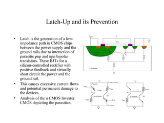
1. Latch-Up and its Prevention
• Latch is the generation of a low-
impedance path in CMOS chips
between the power supply and the
ground rails due to interaction of
parasitic pnp and npn bipolar
transistors. These BJTs for a
silicon-controlled rectifier with
positive feedback and virtually
short circuit the power and the
ground rail.
• This causes excessive current flows
and potential permanent damage to
the devices.
• Analysis of the a CMOS Inverter
CMOS depicting the parasitics.
2. Latch-Up Continued
• The equivalent circuit shown has
Q1 being a vertical double
emmitter pnp transistor whose
base is formed by the n-well with a
high base to collector current gain
(β1).
• Q2 is a lateral double emitter npn
transistor whose base is formed by
the p-type substrate.
• Rwell represents the parasitic
resistance in the n-well structure
whose value ranges from 1KΩ to
20kΩ.
• The substrate resistance Rsub
depends on the substrate structure.
• Assume the Rwell and Rsub are
significantly large so that they
cause open circuit connections, this
results in low current gains and the
currents would be reverse leakage
currents for both the npn and pnp
transistors.
• If some external disturbance
occurs, causing the collector
current of one of the parasitic
transistors to increase, the resulting
feedback loop causes the current
perturbation to be multiplied by
β1.β2
3. Latch-up Continued
• This event triggers the silicon-
controlled rectifier and each
transistor drives the other with
positive feedback eventually
creating and sustaining a low
impedance path between power and
the ground rails resulting in latch-
up.
• For this condition if β1 *β1 is greater
than or equal to 1 both transistors
will continue to conduct saturation
currents even after the triggering
perturbation is no longer available.
• Some causes for latch-up are:
– Slewing of VDD during start-up causing
enough displacement currents due to
well junction capacitance in the substrate
and well.
– Large currents in the parasitic silicon-
controlled rectifier in CMOS chips can
occur when the input or output signal
swings either far beyond the VDD level
or far below VSS level, injecting a
triggering current. Impedance
mismatches in transmission lines can
cause such disturbances in high speed
circuits.
– Electrostatic Discharge stress can cause
latch-up by injecting minority carriers
from the clamping device in the
protection circuit into either the substrate
or the well.
– Sudden transient in power or ground
buses may cause latch-up.
4. Guidelines For Avoiding Latch-Up
• Reduce the BJT gains by lowering the
minority carrier lifetime through Gold
doping of the substrate (solution might
cause excessive leakage currents).
• Use p+
guardband rings connected to
ground around nMOS transistors and n+
guard rings connected to VDD around
pMOS transistors to reduce Rw and Rsub
and to capture injected minority carriers
before they reach the base of the
parasitic BJT.
• Place substrate and well contacts as
close as possible to the source
connections of the MOS transistors to
reduce the values of Rw and Rsub.
(solution to be used in your designs)
• Place source diffusion regions for
the pMOS transistors so that they
lie along equipotentials lines when
currents flow between VDD and p-
wells.
• Avoid forward biasing of the
source/drain junctions so as not to
inject high currents , this solution
calls for the use of slightly doped
epitaxial layer on top of the heanily
doped substrate and has the effect
of shunting the lateral currents
from the vertical transistor through
the low resistance substrate.