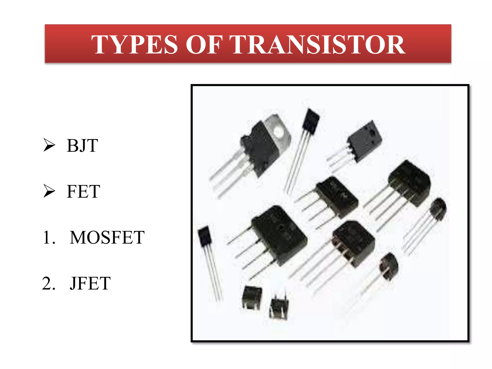
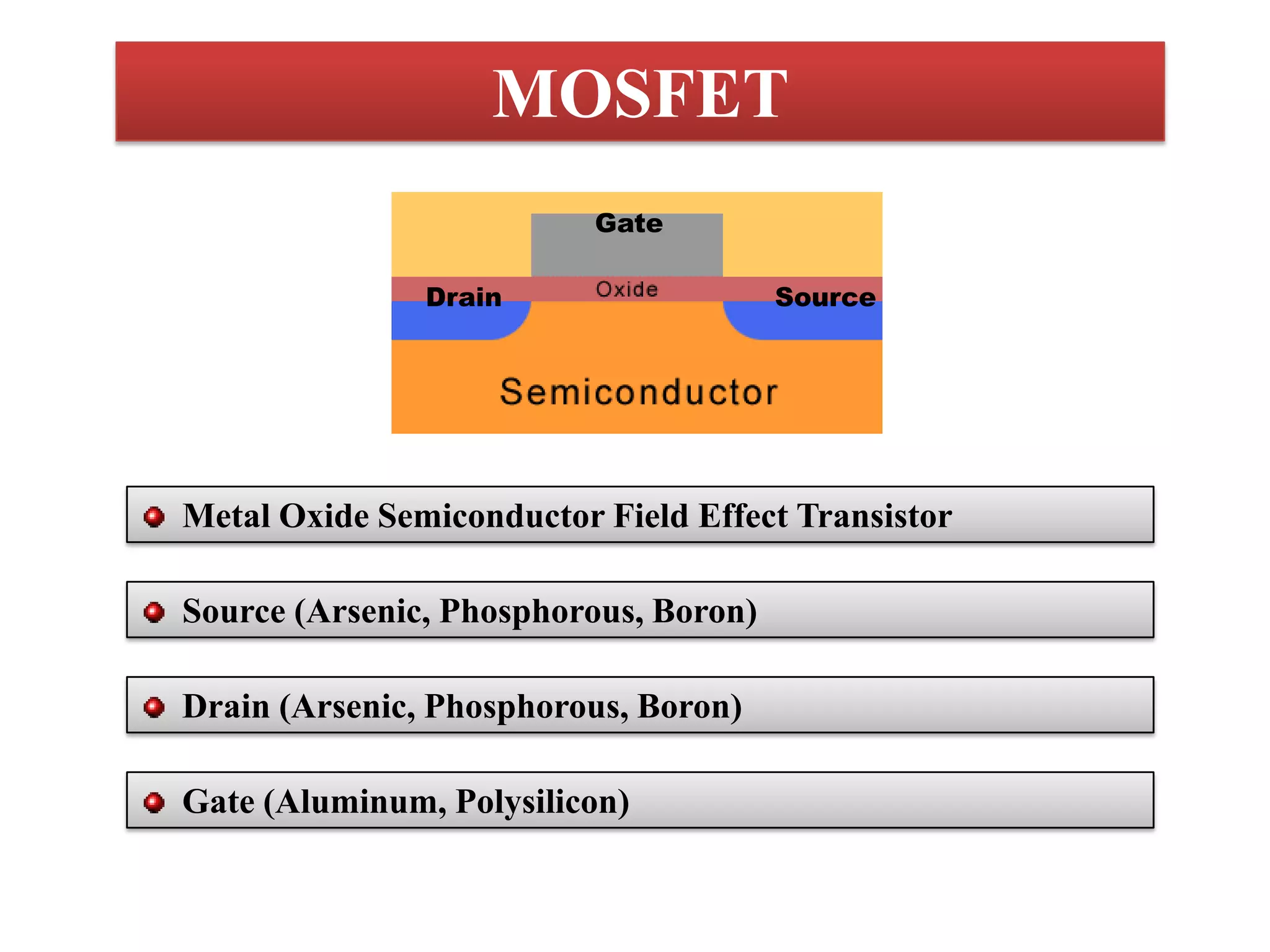
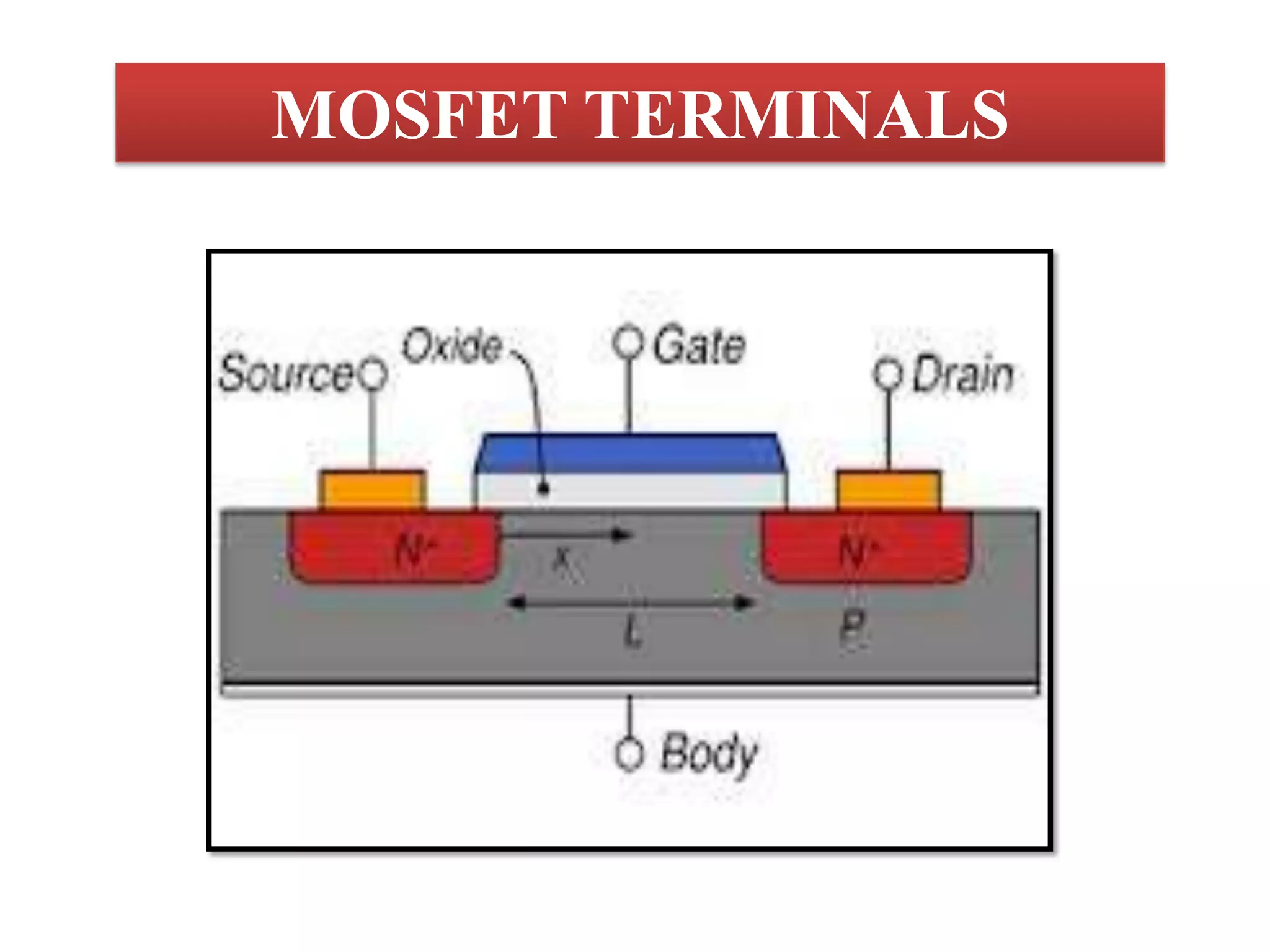
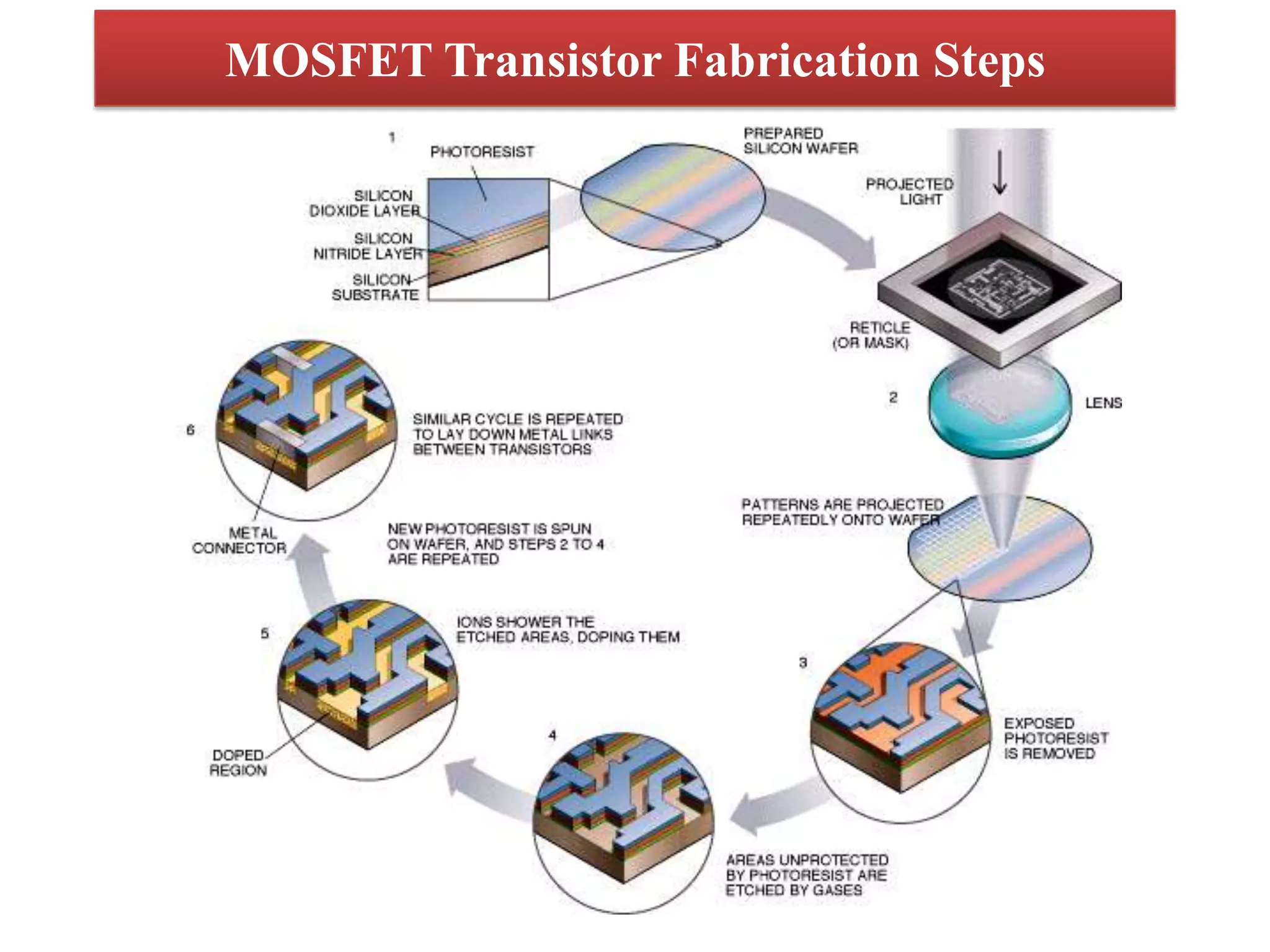
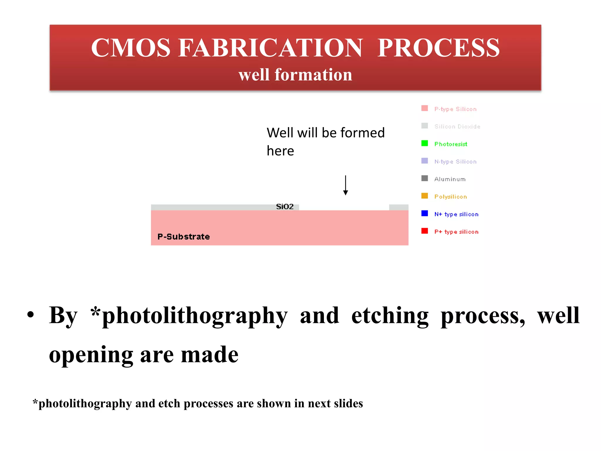
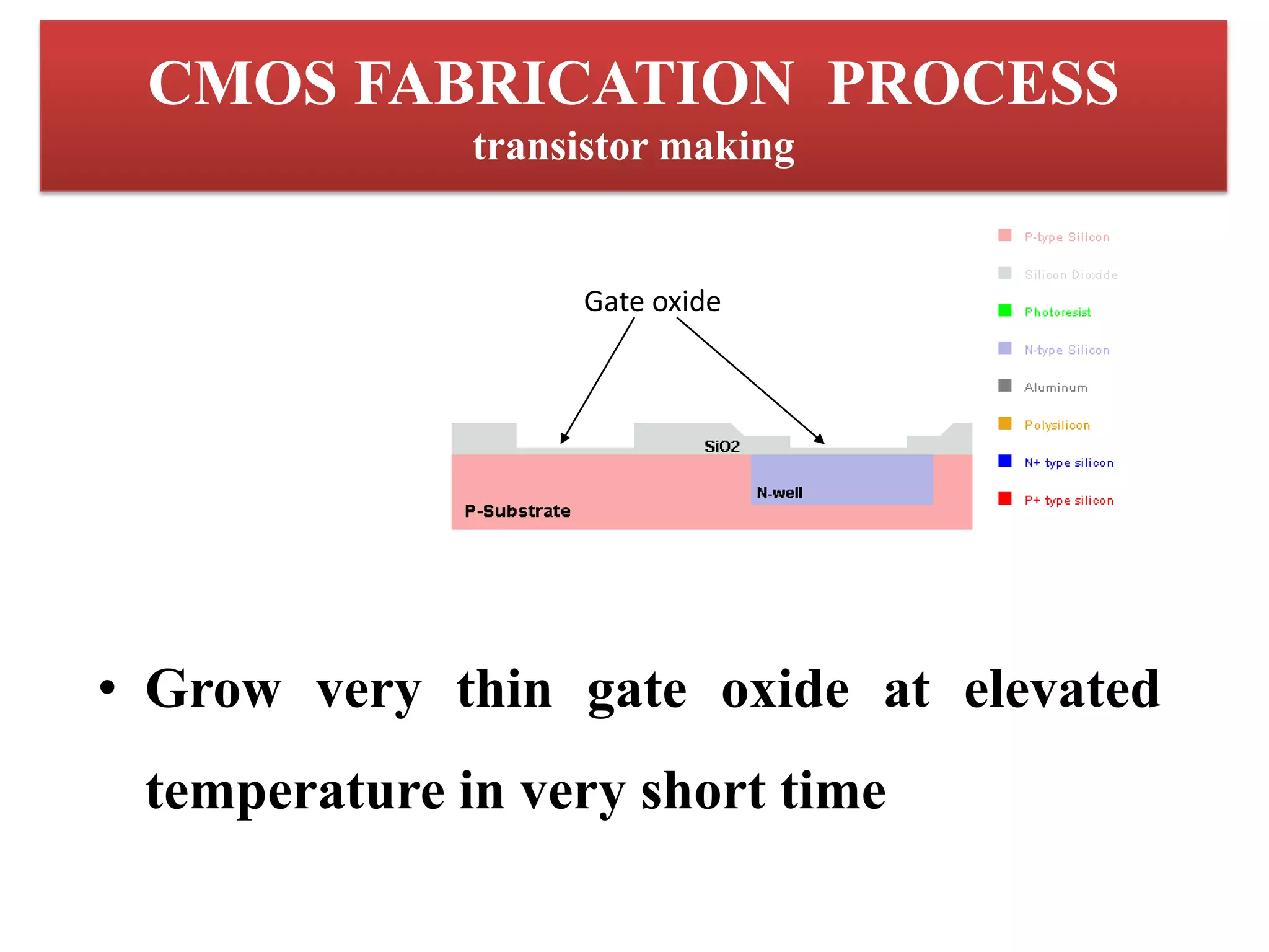
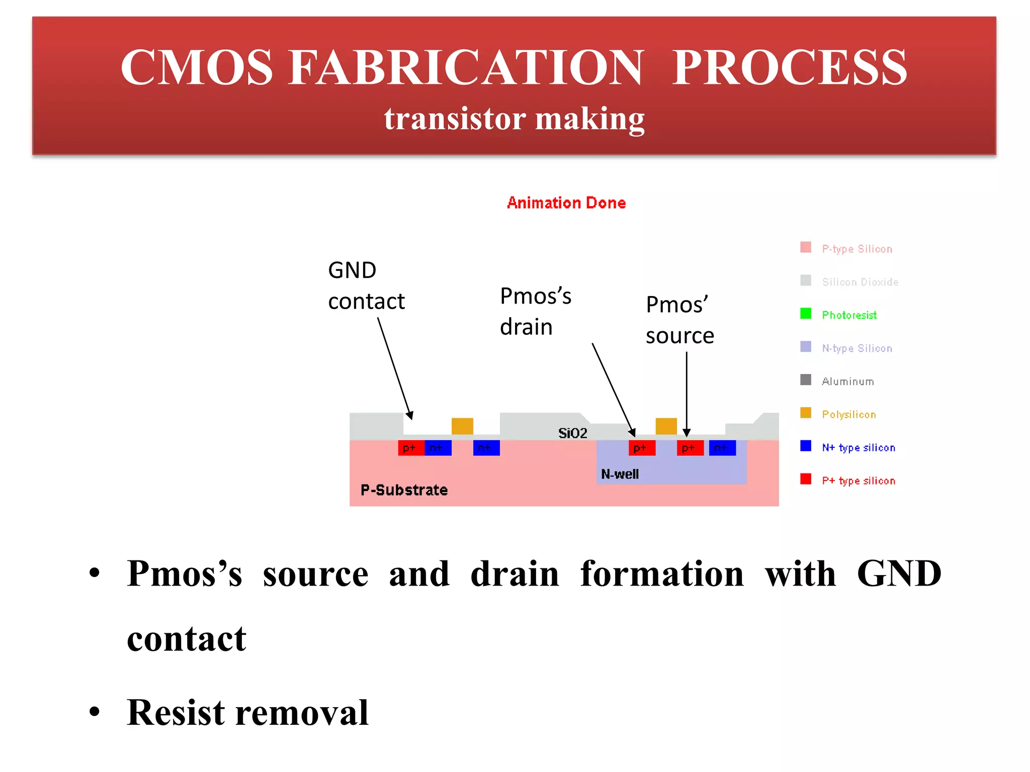
SlideShare a Scribd company logo
1 of 52
NT 2005 MOLECULAR AND
NANOELECTRONICS
MOSFET

BY,
A. POOJA SHUKLA
1821310006
M. Tech (I year)
INTRODUCTION TO
TRANSISTOR
 In 1947 by John Bardeen, Walter Brattain and William Shockley
the transistor revolutionized the field of electronics

 A transistor is a semiconductor device used to amplify and switch
electronic signals and electrical power.
 It is composed of semiconductor material with at least three
terminals for connection to an external circuit.
 The transistor is the fundamental building block of modern
electronic devices.
TYPES OF TRANSISTOR

 BJT
 FET
1. MOSFET
2. JFET
FET TERMINALS SYMBOL
BJT AND FET

BJT

FET
WHAT IS MOSFET….???

 The

metal–oxide–semiconductor

field-effect

transistor

(MOSFET, MOS-FET, or MOS FET) is a transistor used for
amplifying or switching electronic signals.
MOSFET
Gate
Drain

Source

Metal Oxide Semiconductor Field Effect Transistor
Source (Arsenic, Phosphorous, Boron)
Drain (Arsenic, Phosphorous, Boron)
Gate (Aluminum, Polysilicon)
MOSFET TERMINALS
TYPES OF MOSFET

 n - MOS FET
 p – MOS FET
 CMOS FET
MOSFET TERMINALS
SYMBOL
D

D

G

G
S

NMOS Enhancement

S

NMOS Depletion

D

G

D

G

S

PMOS Enhancement

B
S

NMOS with
Bulk Contact

Channel
MOSFET STRUCTURE

• This device is symmetric, so either of the n+ regions can be source
or drain.
INTO TO FABRICATION…..!!!
•

Photolithography (photo)
–

Process of transferring pattern on mask to photoresist layer on wafer surface (pre-pattern the
chip)

•

Etching
–

Process of permanently removed the unwanted part of design on wafer surface to get the
desired pattern

•

Diffusion
–

Process of introducing dophant layer by movement of dophant atoms from high concentration
to low concentration area at high temperature

•

Ion implantation
–

Process of introducing dophant layer by bombardment of high energy dophant ion in high
electric field chamber

•

Oxidation
–

•

Process of growing thick or thin SiO2 layer depend on oxide application

CMP
–

Process to physically grind flat to have a planar surface for better exposure at photo process.
MOSFET Transistor Fabrication Steps
Building A MOSFET Transistor Using Silicon
It is done. Now, how does it
work?
MOSFET OPERATION
Step 1: Apply Gate Voltage
SiO2 Insulator (Glass)
Gate

Source

Drain
5 volts

holes

N

N

electrons
P
electrons to be
transmitted
Step 2: Excess electrons surface in
channel, holes are repelled.

Step 3: Channel becomes saturated
with electrons. Electrons in source
are able to flow across channel to
Drain.
N-MOSFET
– 4 electrical terminals
• Source
• Drain
• Gate
• Substrate
– Connected to Gnd

Gate

Source

Drain
Substrate (Body)

– Source and drain are only different in their interpretation
• Terminal with lower voltage is the source (by convention)

– Simplified symbol omits the substrate

VG

VS

VD
N-MOSFET
Gate Oxide
Gate
Source

Polysilicon

n+

Drain
n+

p-substrate

Bulk Contact

CROSS-SECTION of NMOS Transistor

P-type substrate
N-type dopant for Source & Drain

Inversion layer is formed to conduct electricity

Field-Oxide
(SiO2)

p+ stopper
N-MOSFET
• NMOS Behavior
– When Gate (VG) is high (i.e. 1) the NMOS transistor acts as a
closed switch
• When VG = 0, the NMOS transistor is an open switch
VG

VS

VG = "low"

VD

VG = "high"
P-MOSFET
– Same 4 electrical terminals
• Source
• Drain
• Gate
• Substrate
– Connected to VDD

Gate

Drain
Substrate (Body)

Source
V DD

– Again, source and drain are only different in their interpretation
• Terminal with higher voltage is the source (by convention)

– Simplified symbol omits the substrate

VG

VS

VD
P-MOSFET
Gate Oxide
Gate
Source

Polysilicon

p+

Drain
p+

n-substrate

Bulk Contact

CROSS-SECTION of PMOS Transistor

N-type substrate
P-type dopant for Source & Drain
Inversion layer is formed to conduct electricity

Field-Oxide
(SiO2)

n+ stopper
P-MOSFET
• PMOS Behavior
– When Gate (VG) is low (i.e. 0) the PMOS transistor acts as a closed
switch
• When VG = 1, the PMOS transistor is an open switch
VG

VS

VG = "high"

VD

VG = "low"
CMOSFET PROCESS FLOW
WELL FORMATION

ISOLATION FORMATION

TRANSISTOR MAKING

INTERCONNECTION

PASSIVATION
CMOSFET

A combination of both NMOS & PMOS technology
Most basic example: inverter
CMOS FABRICATION PROCESS
well formation

• Start with clean p-type substrate (p-type wafer)
CMOS FABRICATION PROCESS
well formation

• Grow epitaxy layer (made from SiO2) as mask

layer for well formation
CMOS FABRICATION PROCESS
well formation
Well will be formed
here

• By *photolithography and etching process, well
opening are made
*photolithography and etch processes are shown in next slides
CMOS FABRICATION PROCESS
photoresist
Si02
P-substrate

• Photoresist coating (C)

UV light

• Masking and exposure under UV
mask
Opaque
area
P-substrate

Transparent
area

light(E)
• Resist dissolved after developed (D)
– Pre-shape the well pattern at resist
layer
ETCHING
• Removing the unwanted
P-substrate

P-substrate

pattern by wet etching

• Resist clean
• Desired pattern formed
CMOS FABRICATION PROCESS
well formation

Phosphorus ion

• Ion bombardment by ion implantation
• SiO2 as mask, uncovered area will exposed to dophant ion
CMOS FABRICATION PROCESS
isolation formation

Thick oxide

• Increase SiO2 thickness by oxidation at high

temperature
• Oxide will electrically isolates nmos and pmos devices
CMOS FABRICATION PROCESS
transistor making

nmos will be
formed here

pmos will be
formed here

LOCOS (isolation structure)

• By photolithography and etching process,
pmos and nmos areas are defined
CMOS FABRICATION PROCESS
transistor making

Gate oxide

• Grow very thin gate oxide at elevated

temperature in very short time
CMOS FABRICATION PROCESS
transistor making

polysilicon

• Deposit polysilicon layer
CMOS FABRICATION PROCESS
transistor making

gate

• Photolithography (photo) and etching to

form gate pattern
CMOS FABRICATION PROCESS
transistor making
Arsenic ion

photoresist

• Photo process to define the nmos’s active (source
and drain) area and VDD contact

• Ion implantation with Arsenic ion for n+ dophant.
• Photoresist and polisilicon gate act as mask
CMOS FABRICATION PROCESS
transistor making

source

drain

VDD
contact

• Nmos’s Source and drain with VDD contact formation
• Resist removal
CMOS FABRICATION PROCESS
transistor making

Boron ion

photoresist

• Photo process to define the GND contact and pmos’s active
area (source and drain)
• Ion implantation with boron ionto have p+ dophant
• Photoresist and gate act as mask
CMOS FABRICATION PROCESS
transistor making

GND
contact

Pmos’s
drain

Pmos’
source

• Pmos’s source and drain formation with GND

contact
• Resist removal
CMOS FABRICATION PROCESS
interconnection

SiO2

• Deposit SiO2 layer through out wafer
surface
CMOS FABRICATION PROCESS
interconnection
contact

• Photo and etching process to make contact
CMOS FABRICATION PROCESS
interconnection
Metal 1

• Metal 1 deposition throughout wafer

surface
CMOS FABRICATION PROCESS
interconnection

• Photo and etching processes to pattern
interconnection
Mask Layout
Mask Layout
Mask Layout
Mask Layout
A’

A

Metal 1
oxide
n+

n+

p+
N-well

p-substrate

p+
THANK YOU…….!!!

More Related Content

What's hot

What's hot (20)

JFET
JFETJFET
JFET
 
Fet basics-1
Fet basics-1Fet basics-1
Fet basics-1
 
MOSFET Discription Presentation
MOSFET Discription PresentationMOSFET Discription Presentation
MOSFET Discription Presentation
 
Cmos fabrication
Cmos fabricationCmos fabrication
Cmos fabrication
 
C-V characteristics of MOS Capacitor
C-V characteristics of MOS CapacitorC-V characteristics of MOS Capacitor
C-V characteristics of MOS Capacitor
 
15 mosfet threshold voltage
15 mosfet threshold voltage15 mosfet threshold voltage
15 mosfet threshold voltage
 
Basics of MOSFET
Basics of MOSFETBasics of MOSFET
Basics of MOSFET
 
Mosfet
MosfetMosfet
Mosfet
 
JFET Construction, Working Principle And V-I Characterstics
JFET Construction, Working Principle And V-I CharactersticsJFET Construction, Working Principle And V-I Characterstics
JFET Construction, Working Principle And V-I Characterstics
 
Mosfet Operation and Charecteristics.
Mosfet Operation and Charecteristics.Mosfet Operation and Charecteristics.
Mosfet Operation and Charecteristics.
 
Field Effect Transistor ppt
Field Effect Transistor pptField Effect Transistor ppt
Field Effect Transistor ppt
 
Presentation on JFET
Presentation on JFETPresentation on JFET
Presentation on JFET
 
Junctionless transistors
Junctionless transistorsJunctionless transistors
Junctionless transistors
 
Types of MOSFET Applications and Working Operation
Types of MOSFET Applications and Working OperationTypes of MOSFET Applications and Working Operation
Types of MOSFET Applications and Working Operation
 
Basics of JFET
Basics of JFETBasics of JFET
Basics of JFET
 
Types of transistors
Types of transistorsTypes of transistors
Types of transistors
 
MOSFETs
MOSFETsMOSFETs
MOSFETs
 
Mosfet
MosfetMosfet
Mosfet
 
Ppt presentation on FET
Ppt presentation on  FETPpt presentation on  FET
Ppt presentation on FET
 
MOSFET....complete PPT
MOSFET....complete PPTMOSFET....complete PPT
MOSFET....complete PPT
 

Viewers also liked (8)

Metal Oxide Semiconductor Fet (Mosfet)
Metal Oxide Semiconductor Fet (Mosfet)Metal Oxide Semiconductor Fet (Mosfet)
Metal Oxide Semiconductor Fet (Mosfet)
 
Mosfet
MosfetMosfet
Mosfet
 
Design of Series Voltage regulator
Design of Series Voltage regulatorDesign of Series Voltage regulator
Design of Series Voltage regulator
 
Voltage series feedback pair
Voltage series feedback pairVoltage series feedback pair
Voltage series feedback pair
 
Voltage series feedback pair
Voltage series feedback pairVoltage series feedback pair
Voltage series feedback pair
 
JFET
JFETJFET
JFET
 
Feedback amplifiers
Feedback  amplifiersFeedback  amplifiers
Feedback amplifiers
 
Feedback amplifiers
Feedback amplifiersFeedback amplifiers
Feedback amplifiers
 

Similar to Mosfet

Metal oxide-semiconductorfetmosfet-090615015822-phpapp02
Metal oxide-semiconductorfetmosfet-090615015822-phpapp02Metal oxide-semiconductorfetmosfet-090615015822-phpapp02
Metal oxide-semiconductorfetmosfet-090615015822-phpapp02
zambaredn
 
Seminar: Fabrication and Characteristics of CMOS
Seminar: Fabrication and Characteristics of CMOSSeminar: Fabrication and Characteristics of CMOS
Seminar: Fabrication and Characteristics of CMOS
Jay Baxi
 
VLSI-mosfet-construction engineering ECE
VLSI-mosfet-construction engineering ECEVLSI-mosfet-construction engineering ECE
VLSI-mosfet-construction engineering ECE
jpradha86
 

Similar to Mosfet (20)

lecture-1.pdf
lecture-1.pdflecture-1.pdf
lecture-1.pdf
 
FET
FETFET
FET
 
20EC602 VLSI Design.ppt
20EC602 VLSI Design.ppt20EC602 VLSI Design.ppt
20EC602 VLSI Design.ppt
 
layout.pdf
layout.pdflayout.pdf
layout.pdf
 
Mosfet
MosfetMosfet
Mosfet
 
Metal oxide-semiconductorfetmosfet-090615015822-phpapp02
Metal oxide-semiconductorfetmosfet-090615015822-phpapp02Metal oxide-semiconductorfetmosfet-090615015822-phpapp02
Metal oxide-semiconductorfetmosfet-090615015822-phpapp02
 
Special semiconductor devices
Special semiconductor devicesSpecial semiconductor devices
Special semiconductor devices
 
Mosfet
MosfetMosfet
Mosfet
 
Mosfets assignment
Mosfets assignmentMosfets assignment
Mosfets assignment
 
VLSIM11.pptx
VLSIM11.pptxVLSIM11.pptx
VLSIM11.pptx
 
CMOS_design.ppt
CMOS_design.pptCMOS_design.ppt
CMOS_design.ppt
 
Mosfets
MosfetsMosfets
Mosfets
 
ELCTRONIC COMPONENR.pptx
ELCTRONIC COMPONENR.pptxELCTRONIC COMPONENR.pptx
ELCTRONIC COMPONENR.pptx
 
Mosfet
MosfetMosfet
Mosfet
 
Seminar: Fabrication and Characteristics of CMOS
Seminar: Fabrication and Characteristics of CMOSSeminar: Fabrication and Characteristics of CMOS
Seminar: Fabrication and Characteristics of CMOS
 
Vlsi ppt priyanka
Vlsi ppt priyankaVlsi ppt priyanka
Vlsi ppt priyanka
 
PRESENTATION MOSFET
PRESENTATION MOSFETPRESENTATION MOSFET
PRESENTATION MOSFET
 
Introduction to active and passive components
Introduction to active and passive components Introduction to active and passive components
Introduction to active and passive components
 
Transistor, fotodiode, dan diode pemencar [14]
Transistor, fotodiode, dan diode pemencar [14]Transistor, fotodiode, dan diode pemencar [14]
Transistor, fotodiode, dan diode pemencar [14]
 
VLSI-mosfet-construction engineering ECE
VLSI-mosfet-construction engineering ECEVLSI-mosfet-construction engineering ECE
VLSI-mosfet-construction engineering ECE
 

More from Pooja Shukla (13)

Biosensors
BiosensorsBiosensors
Biosensors
 
One time research and longitudinal research
One time research and longitudinal researchOne time research and longitudinal research
One time research and longitudinal research
 
Nanotechnology in sunscreen uv protection
Nanotechnology in sunscreen uv protectionNanotechnology in sunscreen uv protection
Nanotechnology in sunscreen uv protection
 
Double gate mosfet
Double gate mosfetDouble gate mosfet
Double gate mosfet
 
Magnetism data addressing
Magnetism data addressingMagnetism data addressing
Magnetism data addressing
 
Self assembly
Self assemblySelf assembly
Self assembly
 
SIMULATION OF TEMPERATURE SENSOR USING LABVIEW
SIMULATION OF TEMPERATURE SENSOR USING LABVIEWSIMULATION OF TEMPERATURE SENSOR USING LABVIEW
SIMULATION OF TEMPERATURE SENSOR USING LABVIEW
 
Gsm
GsmGsm
Gsm
 
Light wave-system-3855513
Light wave-system-3855513Light wave-system-3855513
Light wave-system-3855513
 
Wireless communicationpe-3855140
Wireless communicationpe-3855140Wireless communicationpe-3855140
Wireless communicationpe-3855140
 
Ppt nc
Ppt ncPpt nc
Ppt nc
 
Fabrication of silicon on insulator (soi)
Fabrication of silicon on insulator (soi)Fabrication of silicon on insulator (soi)
Fabrication of silicon on insulator (soi)
 
Vlsi
VlsiVlsi
Vlsi
 

Recently uploaded

Cloud Frontiers: A Deep Dive into Serverless Spatial Data and FME
Cloud Frontiers:  A Deep Dive into Serverless Spatial Data and FMECloud Frontiers:  A Deep Dive into Serverless Spatial Data and FME
Cloud Frontiers: A Deep Dive into Serverless Spatial Data and FME
Safe Software
 

Recently uploaded (20)

[BuildWithAI] Introduction to Gemini.pdf
[BuildWithAI] Introduction to Gemini.pdf[BuildWithAI] Introduction to Gemini.pdf
[BuildWithAI] Introduction to Gemini.pdf
 
"I see eyes in my soup": How Delivery Hero implemented the safety system for ...
"I see eyes in my soup": How Delivery Hero implemented the safety system for ..."I see eyes in my soup": How Delivery Hero implemented the safety system for ...
"I see eyes in my soup": How Delivery Hero implemented the safety system for ...
 
Less Is More: Utilizing Ballerina to Architect a Cloud Data Platform
Less Is More: Utilizing Ballerina to Architect a Cloud Data PlatformLess Is More: Utilizing Ballerina to Architect a Cloud Data Platform
Less Is More: Utilizing Ballerina to Architect a Cloud Data Platform
 
Introduction to use of FHIR Documents in ABDM
Introduction to use of FHIR Documents in ABDMIntroduction to use of FHIR Documents in ABDM
Introduction to use of FHIR Documents in ABDM
 
Decarbonising Commercial Real Estate: The Role of Operational Performance
Decarbonising Commercial Real Estate: The Role of Operational PerformanceDecarbonising Commercial Real Estate: The Role of Operational Performance
Decarbonising Commercial Real Estate: The Role of Operational Performance
 
Connector Corner: Accelerate revenue generation using UiPath API-centric busi...
Connector Corner: Accelerate revenue generation using UiPath API-centric busi...Connector Corner: Accelerate revenue generation using UiPath API-centric busi...
Connector Corner: Accelerate revenue generation using UiPath API-centric busi...
 
Six Myths about Ontologies: The Basics of Formal Ontology
Six Myths about Ontologies: The Basics of Formal OntologySix Myths about Ontologies: The Basics of Formal Ontology
Six Myths about Ontologies: The Basics of Formal Ontology
 
Polkadot JAM Slides - Token2049 - By Dr. Gavin Wood
Polkadot JAM Slides - Token2049 - By Dr. Gavin WoodPolkadot JAM Slides - Token2049 - By Dr. Gavin Wood
Polkadot JAM Slides - Token2049 - By Dr. Gavin Wood
 
AWS Community Day CPH - Three problems of Terraform
AWS Community Day CPH - Three problems of TerraformAWS Community Day CPH - Three problems of Terraform
AWS Community Day CPH - Three problems of Terraform
 
ChatGPT and Beyond - Elevating DevOps Productivity
ChatGPT and Beyond - Elevating DevOps ProductivityChatGPT and Beyond - Elevating DevOps Productivity
ChatGPT and Beyond - Elevating DevOps Productivity
 
CNIC Information System with Pakdata Cf In Pakistan
CNIC Information System with Pakdata Cf In PakistanCNIC Information System with Pakdata Cf In Pakistan
CNIC Information System with Pakdata Cf In Pakistan
 
Navigating Identity and Access Management in the Modern Enterprise
Navigating Identity and Access Management in the Modern EnterpriseNavigating Identity and Access Management in the Modern Enterprise
Navigating Identity and Access Management in the Modern Enterprise
 
JavaScript Usage Statistics 2024 - The Ultimate Guide
JavaScript Usage Statistics 2024 - The Ultimate GuideJavaScript Usage Statistics 2024 - The Ultimate Guide
JavaScript Usage Statistics 2024 - The Ultimate Guide
 
Repurposing LNG terminals for Hydrogen Ammonia: Feasibility and Cost Saving
Repurposing LNG terminals for Hydrogen Ammonia: Feasibility and Cost SavingRepurposing LNG terminals for Hydrogen Ammonia: Feasibility and Cost Saving
Repurposing LNG terminals for Hydrogen Ammonia: Feasibility and Cost Saving
 
Platformless Horizons for Digital Adaptability
Platformless Horizons for Digital AdaptabilityPlatformless Horizons for Digital Adaptability
Platformless Horizons for Digital Adaptability
 
Understanding the FAA Part 107 License ..
Understanding the FAA Part 107 License ..Understanding the FAA Part 107 License ..
Understanding the FAA Part 107 License ..
 
Cloud Frontiers: A Deep Dive into Serverless Spatial Data and FME
Cloud Frontiers:  A Deep Dive into Serverless Spatial Data and FMECloud Frontiers:  A Deep Dive into Serverless Spatial Data and FME
Cloud Frontiers: A Deep Dive into Serverless Spatial Data and FME
 
WSO2 Micro Integrator for Enterprise Integration in a Decentralized, Microser...
WSO2 Micro Integrator for Enterprise Integration in a Decentralized, Microser...WSO2 Micro Integrator for Enterprise Integration in a Decentralized, Microser...
WSO2 Micro Integrator for Enterprise Integration in a Decentralized, Microser...
 
Design and Development of a Provenance Capture Platform for Data Science
Design and Development of a Provenance Capture Platform for Data ScienceDesign and Development of a Provenance Capture Platform for Data Science
Design and Development of a Provenance Capture Platform for Data Science
 
AI in Action: Real World Use Cases by Anitaraj
AI in Action: Real World Use Cases by AnitarajAI in Action: Real World Use Cases by Anitaraj
AI in Action: Real World Use Cases by Anitaraj
 

Mosfet