Downloaded 138 times
![Introduction to TCAD
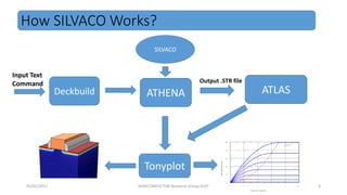
• Technology CAD (Technology Computer Aided Design) is a branch of
electronic design automation that models semiconductor fabrication
and semiconductor device operation.
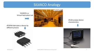
• The modeling of the fabrication is termed Process TCAD [ATHENA In
SILVACO],
• Modeling of the device operation is termed Device TCAD[ATLAS In
SILVACO].
05/01/2017 SEMICONDUCTOR Research Group,SUST 3](https://image.slidesharecdn.com/introductiononsilvaco-170105165750/85/Introduction-to-SILVACO-and-MOSFET-Simulation-technique-3-320.jpg)
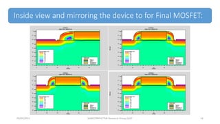
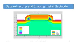
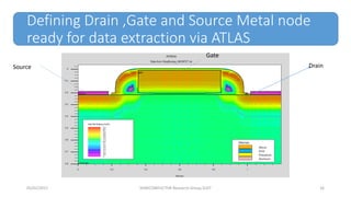


The document discusses simulation of MOSFETs using SILVACO TCAD software. It provides an overview of SILVACO and the process and device simulation capabilities. The document then walks through the steps of simulating a MOSFET fabrication process using ATHENA and defining the materials and doping steps. It describes analyzing the fabricated device using ATLAS to extract characteristics and define contacts before discussing plans to simulate additional devices by varying parameters.


![Topic 1 ee201[1]](https://cdn.slidesharecdn.com/ss_thumbnails/topic1ee2011-151016080603-lva1-app6891-thumbnail.jpg?width=640&height=640&fit=bounds)


