Downloaded 30 times

![DOUBLE GATE FET
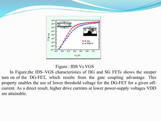
Double-gate (DG) FETs, in which a second gate is added
opposite the traditional (first) gate, have better control over
short-channel effects [SCEs]. SCE limits the minimum channel
length at which an FET is electrically well behaved.
Figure :schematically illustrates the advantage of DG-FETs.](https://image.slidesharecdn.com/17304013-navya-200209170047/85/Finfet-Technology-6-320.jpg)


This document discusses FinFET technology. It begins with an introduction to FinFETs, explaining that they are a type of double-gate CMOS that offers advantages over traditional CMOS for scaling to short gate lengths. It then discusses why FinFET technology is needed as traditional CMOS scaling faces challenges from subthreshold and gate leakage. It provides details on double-gate FET structure and operation, including how it controls short-channel effects better than single-gate FETs. It also covers FinFET features, applications, challenges and concludes that FinFETs can help continue CMOS scaling if key issues like fin patterning and gate work functions are addressed.