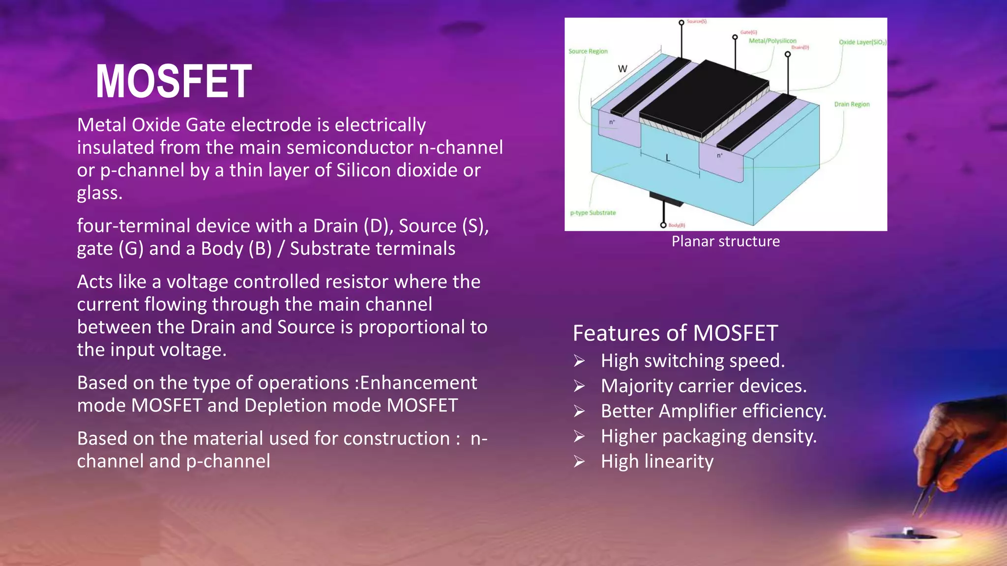
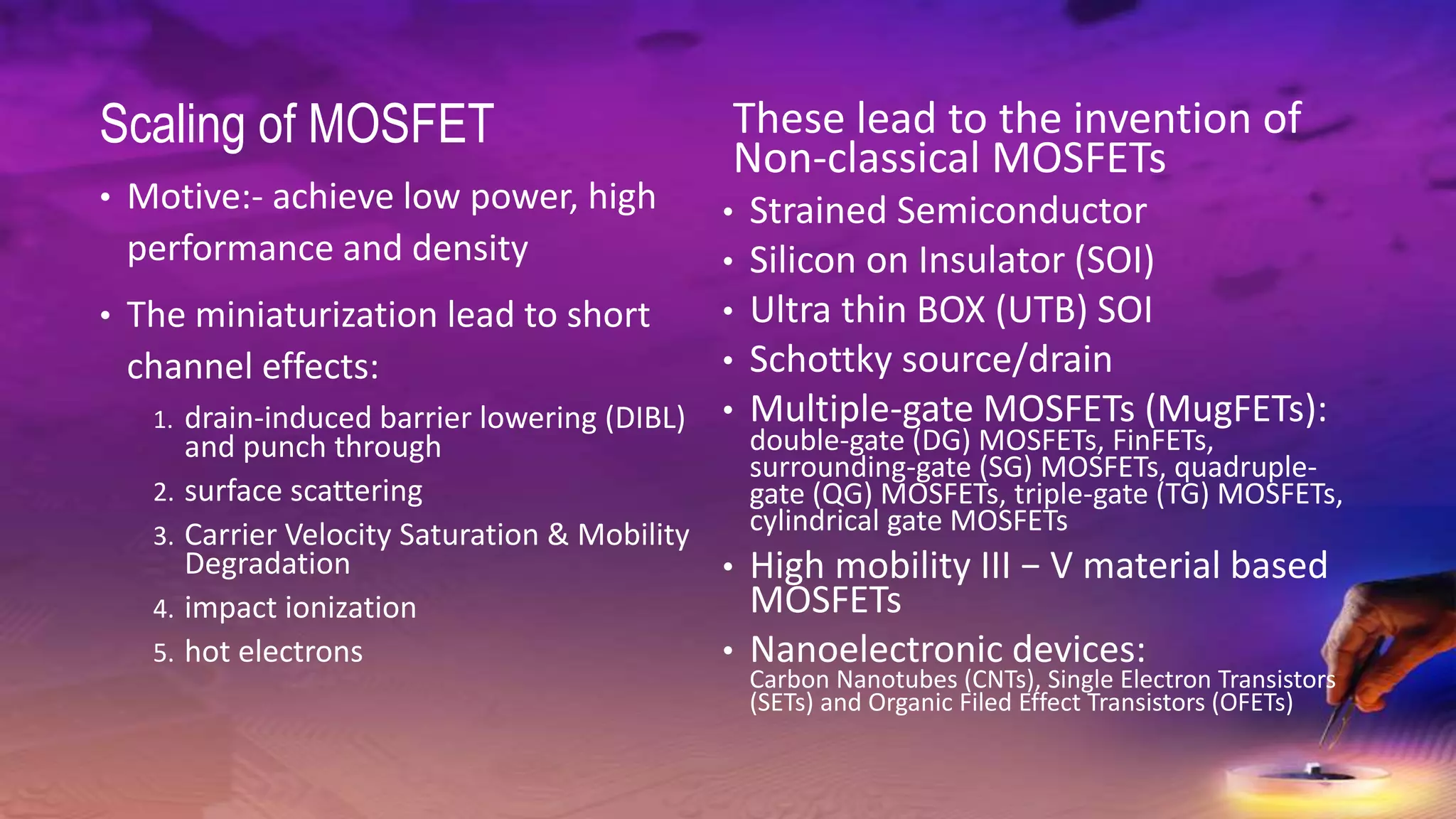
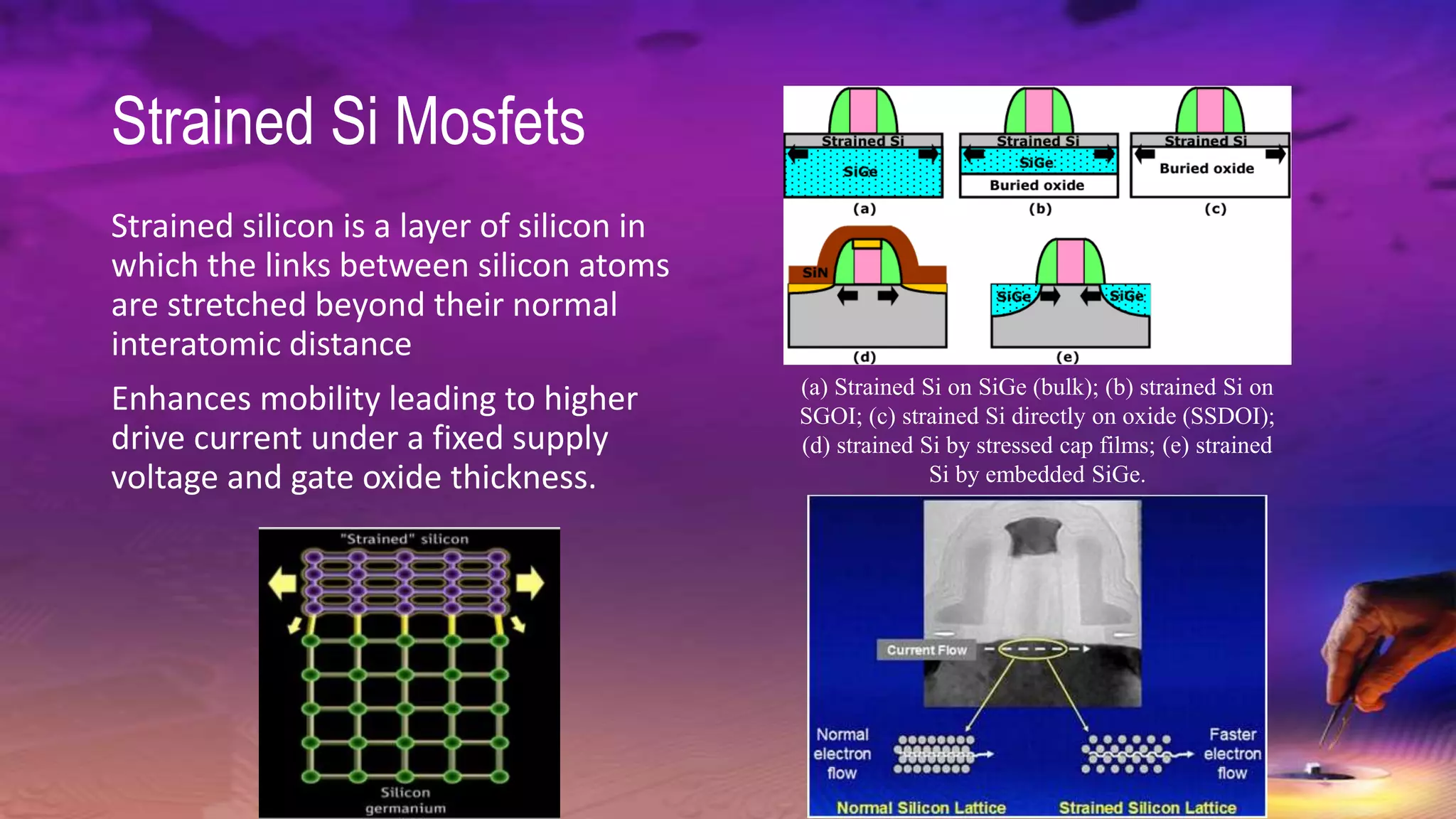
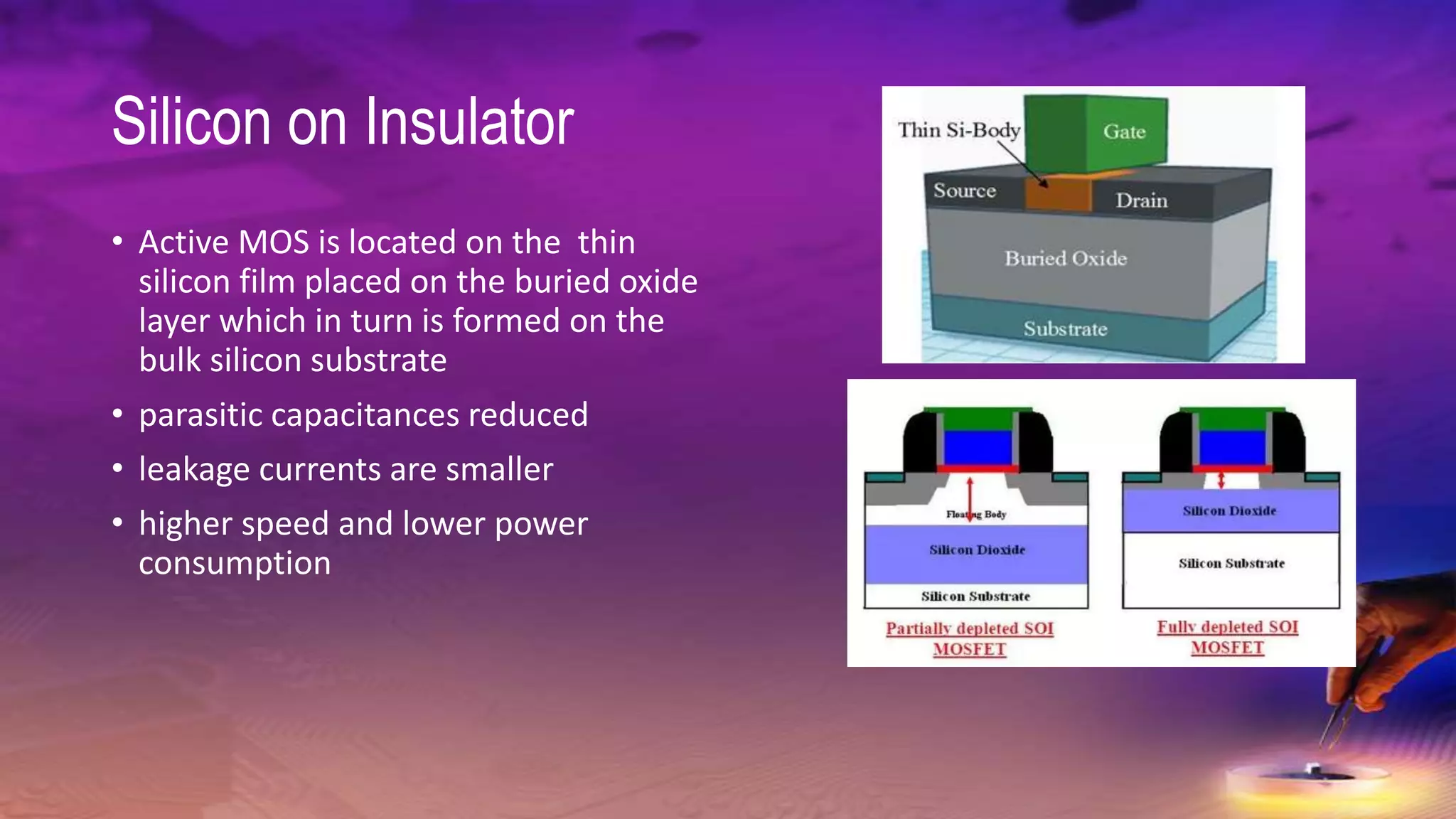
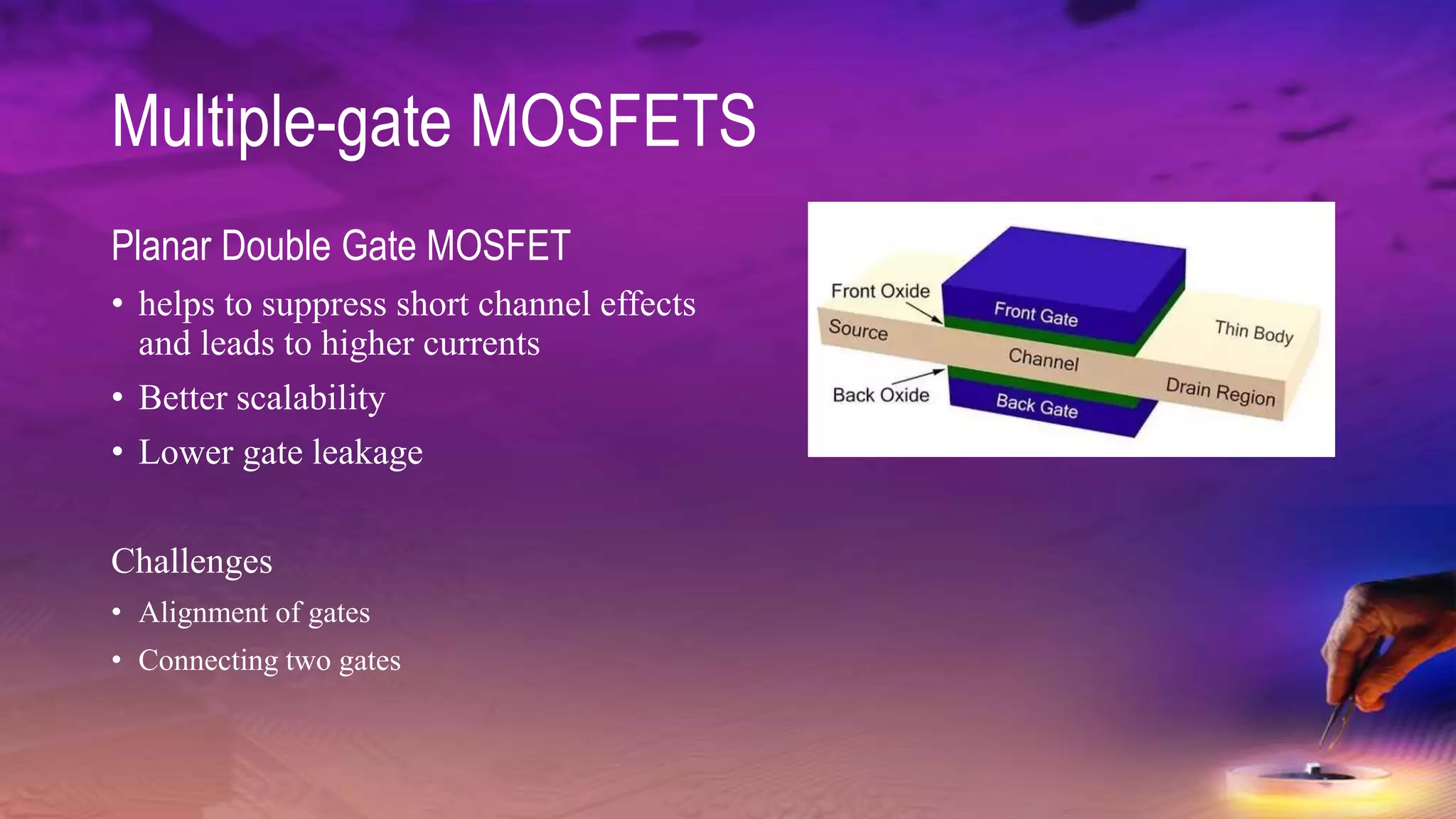
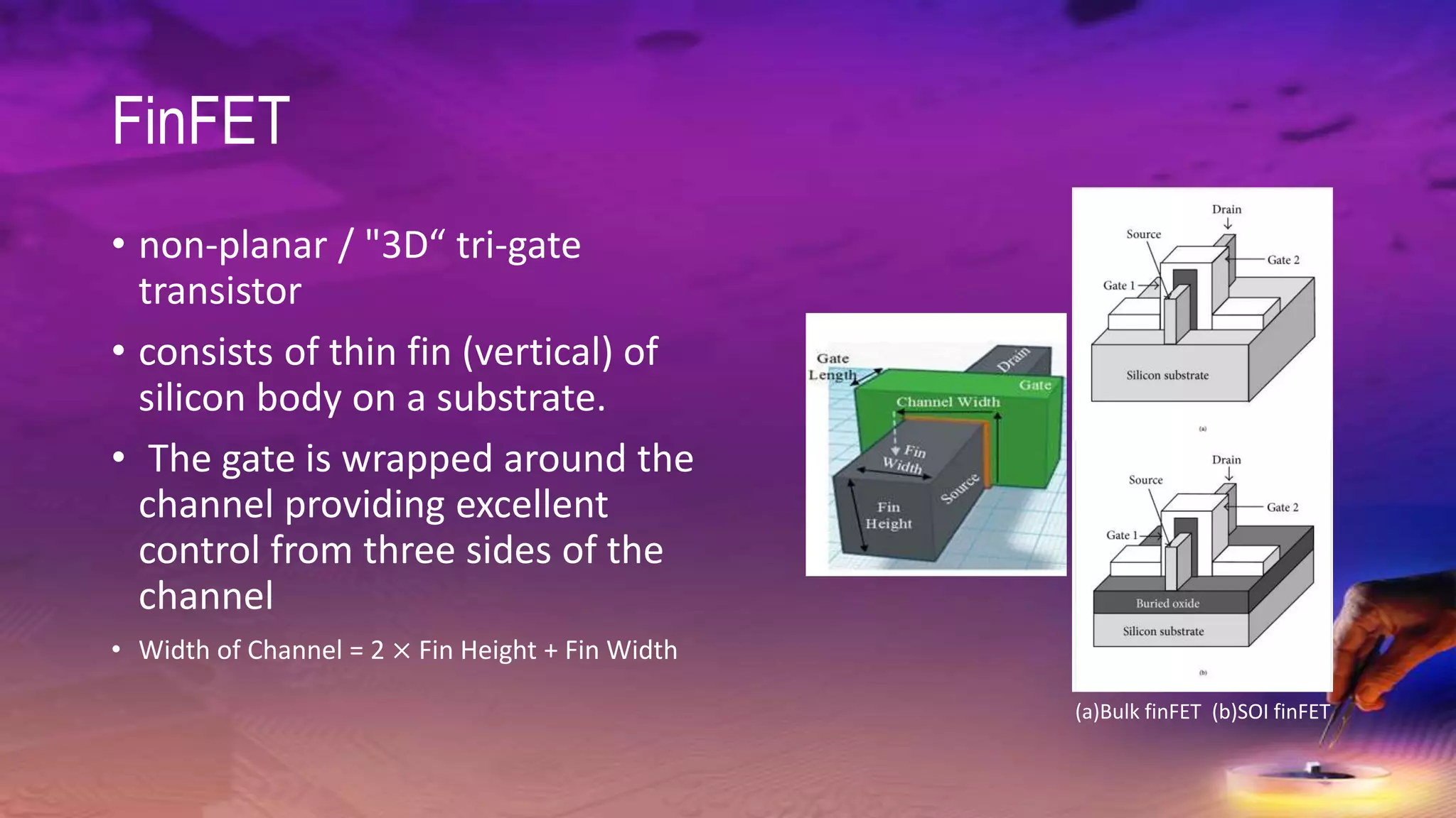
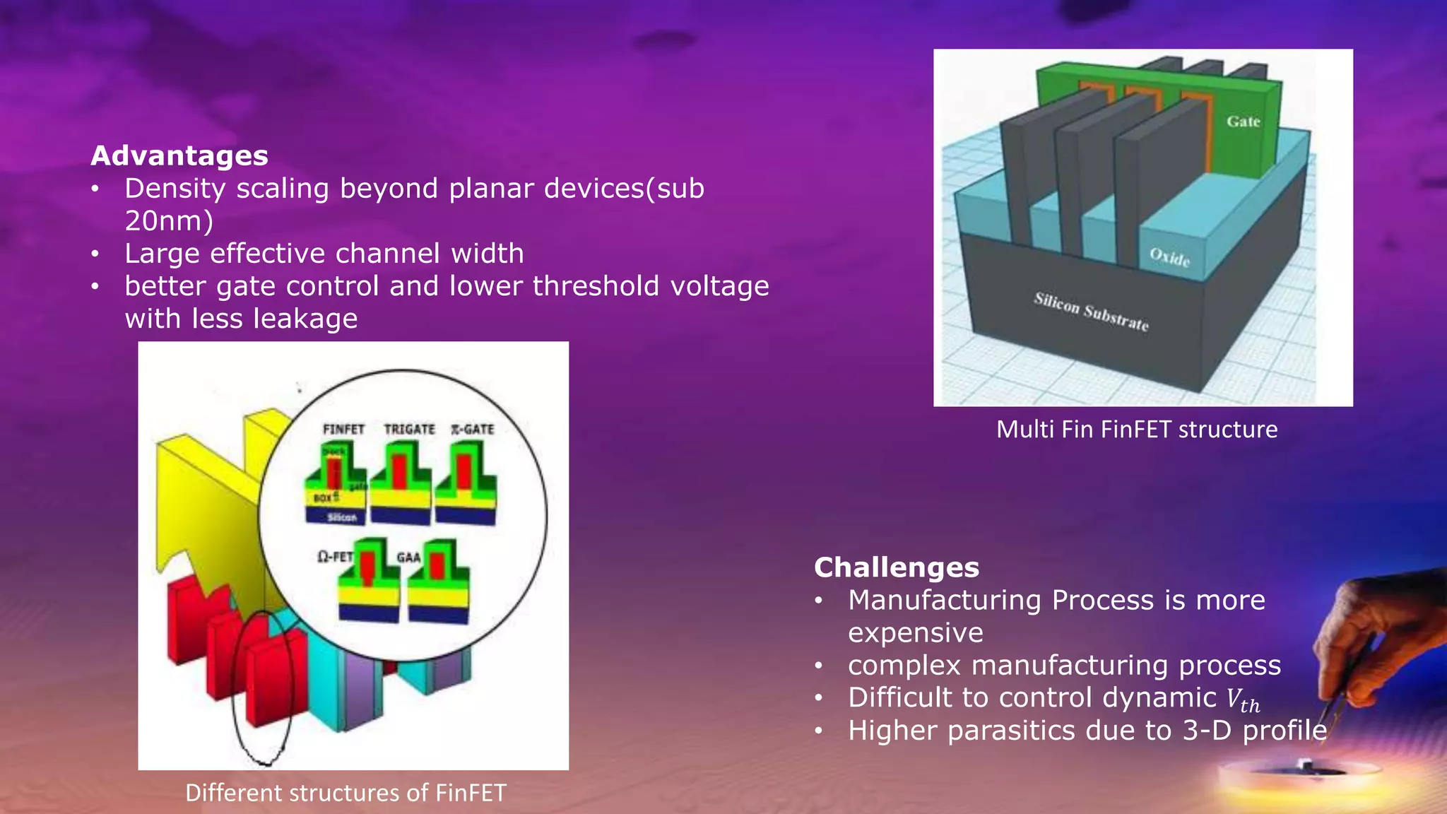
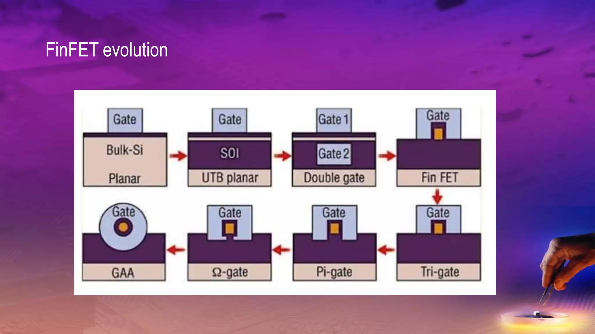
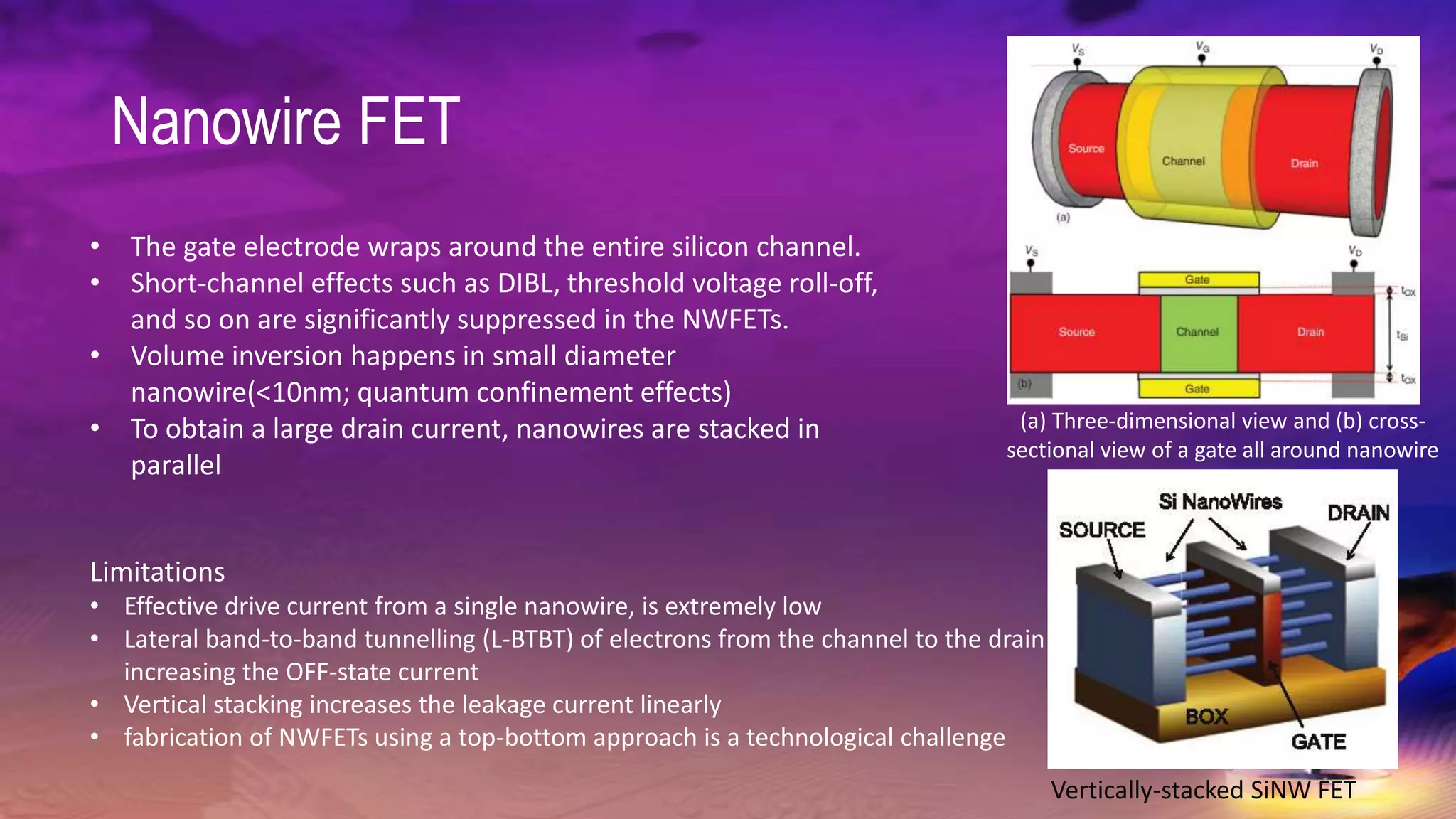
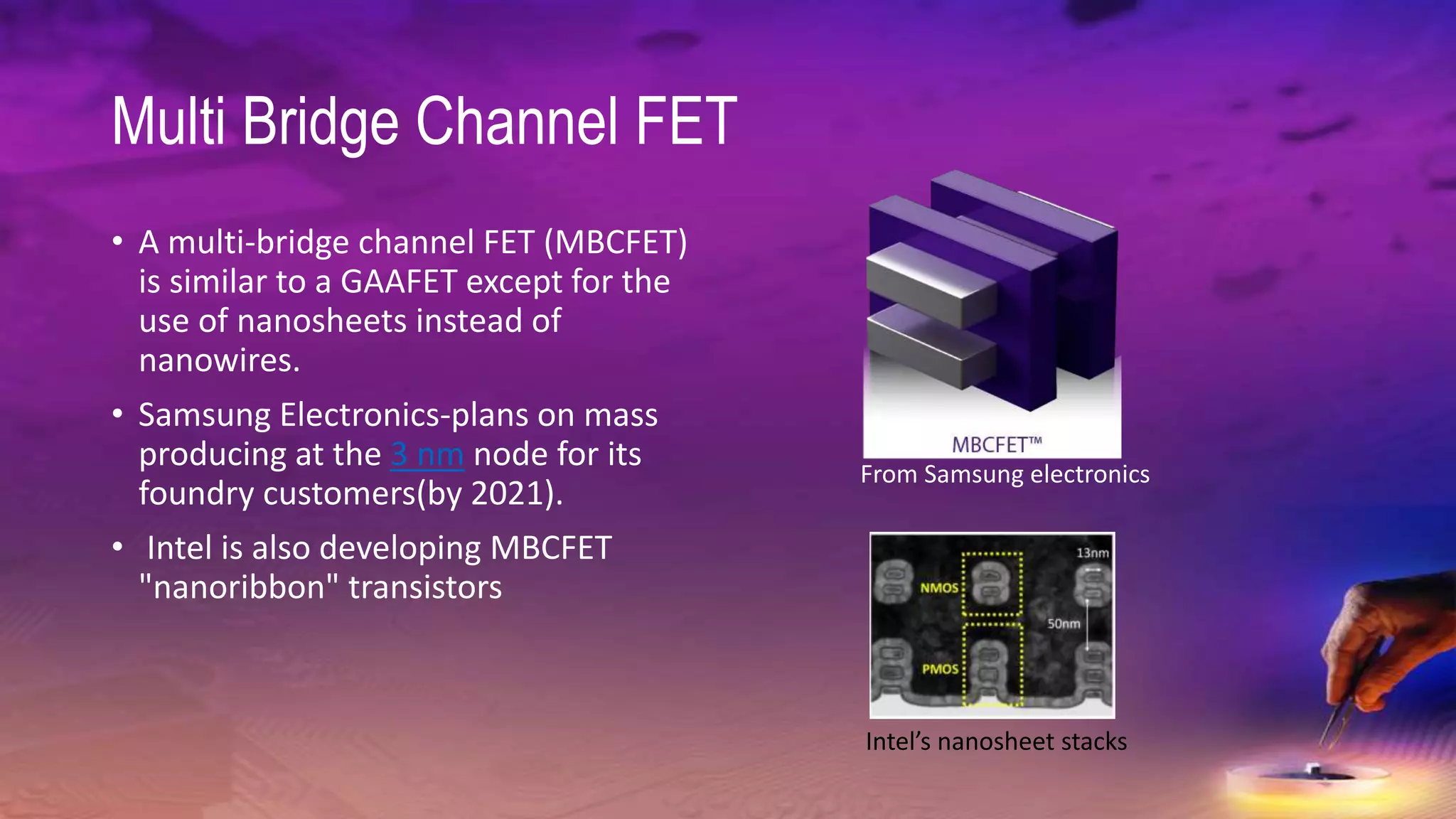
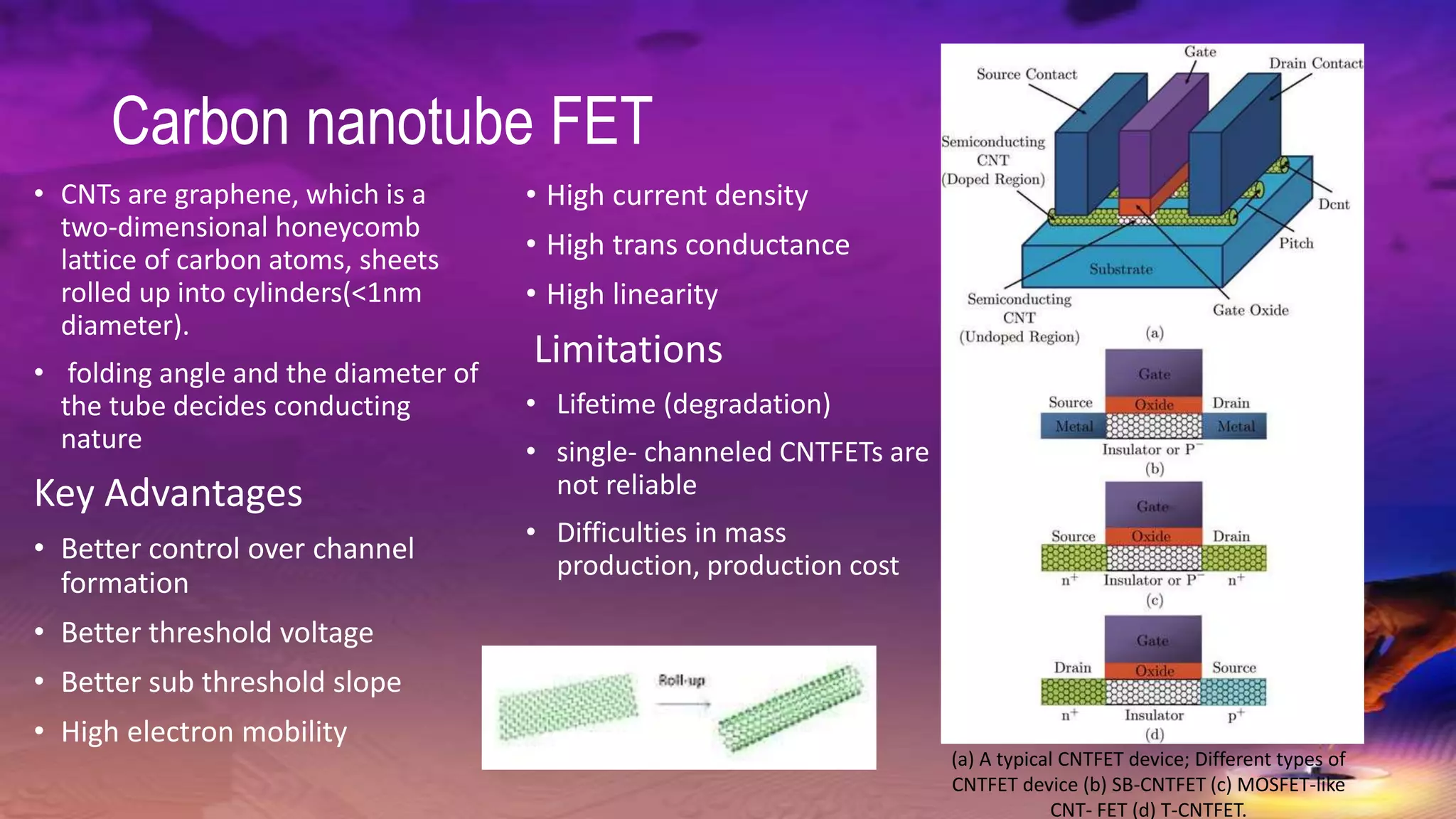
Various MOSFET Structures at a glance
Denita Rose Tom
20304006
Pondicherry University
MOSFET
Metal Oxide Gate electrode is electrically
insulated from the main semiconductor n-channel
or p-channel by a thin layer of Silicon dioxide or
glass.
four-terminal device with a Drain (D), Source (S),
gate (G) and a Body (B) / Substrate terminals
Acts like a voltage controlled resistor where the
current flowing through the main channel
between the Drain and Source is proportional to
the input voltage.
Based on the type of operations :Enhancement
mode MOSFET and Depletion mode MOSFET
Based on the material used for construction : n-
channel and p-channel
Planar structure
Features of MOSFET
 High switching speed.
 Majority carrier devices.
 Better Amplifier efficiency.
 Higher packaging density.
 High linearity
Scaling of MOSFET
• Motive:- achieve low power, high
performance and density
• The miniaturization lead to short
channel effects:
1. drain-induced barrier lowering (DIBL)
and punch through
2. surface scattering
3. Carrier Velocity Saturation & Mobility
Degradation
4. impact ionization
5. hot electrons
These lead to the invention of
Non-classical MOSFETs
• Strained Semiconductor
• Silicon on Insulator (SOI)
• Ultra thin BOX (UTB) SOI
• Schottky source/drain
• Multiple-gate MOSFETs (MugFETs):
double-gate (DG) MOSFETs, FinFETs,
surrounding-gate (SG) MOSFETs, quadruple-
gate (QG) MOSFETs, triple-gate (TG) MOSFETs,
cylindrical gate MOSFETs
• High mobility III − V material based
MOSFETs
• Nanoelectronic devices:
Carbon Nanotubes (CNTs), Single Electron Transistors
(SETs) and Organic Filed Effect Transistors (OFETs)
Strained Si Mosfets
Strained silicon is a layer of silicon in
which the links between silicon atoms
are stretched beyond their normal
interatomic distance
Enhances mobility leading to higher
drive current under a fixed supply
voltage and gate oxide thickness.
(a) Strained Si on SiGe (bulk); (b) strained Si on
SGOI; (c) strained Si directly on oxide (SSDOI);
(d) strained Si by stressed cap films; (e) strained
Si by embedded SiGe.
Silicon on Insulator
• Active MOS is located on the thin
silicon film placed on the buried oxide
layer which in turn is formed on the
bulk silicon substrate
• parasitic capacitances reduced
• leakage currents are smaller
• higher speed and lower power
consumption
Multiple-gate MOSFETS
Planar Double Gate MOSFET
• helps to suppress short channel effects
and leads to higher currents
• Better scalability
• Lower gate leakage
Challenges
• Alignment of gates
• Connecting two gates
FinFET
• non-planar / "3D“ tri-gate
transistor
• consists of thin fin (vertical) of
silicon body on a substrate.
• The gate is wrapped around the
channel providing excellent
control from three sides of the
channel
• Width of Channel = 2 × Fin Height + Fin Width
(a)Bulk finFET (b)SOI finFET
Multi Fin FinFET structure
Advantages
• Density scaling beyond planar devices(sub
20nm)
• Large effective channel width
• better gate control and lower threshold voltage
with less leakage
Challenges
• Manufacturing Process is more
expensive
• complex manufacturing process
• Difficult to control dynamic 𝑉𝑡ℎ
• Higher parasitics due to 3-D profile
Different structures of FinFET
FinFET evolution
Nanowire FET
• The gate electrode wraps around the entire silicon channel.
• Short-channel effects such as DIBL, threshold voltage roll-off,
and so on are significantly suppressed in the NWFETs.
• Volume inversion happens in small diameter
nanowire(<10nm; quantum confinement effects)
• To obtain a large drain current, nanowires are stacked in
parallel
Limitations
• Effective drive current from a single nanowire, is extremely low
• Lateral band-to-band tunnelling (L-BTBT) of electrons from the channel to the drain
increasing the OFF-state current
• Vertical stacking increases the leakage current linearly
• fabrication of NWFETs using a top-bottom approach is a technological challenge
(a) Three-dimensional view and (b) cross-
sectional view of a gate all around nanowire
Vertically-stacked SiNW FET
Multi Bridge Channel FET
• A multi-bridge channel FET (MBCFET)
is similar to a GAAFET except for the
use of nanosheets instead of
nanowires.
• Samsung Electronics-plans on mass
producing at the 3 nm node for its
foundry customers(by 2021).
• Intel is also developing MBCFET
"nanoribbon" transistors
Intel’s nanosheet stacks
From Samsung electronics
Carbon nanotube FET
• CNTs are graphene, which is a
two-dimensional honeycomb
lattice of carbon atoms, sheets
rolled up into cylinders(<1nm
diameter).
• folding angle and the diameter of
the tube decides conducting
nature
Key Advantages
• Better control over channel
formation
• Better threshold voltage
• Better sub threshold slope
• High electron mobility
• High current density
• High trans conductance
• High linearity
Limitations
• Lifetime (degradation)
• single- channeled CNTFETs are
not reliable
• Difficulties in mass
production, production cost
(a) A typical CNTFET device; Different types of
CNTFET device (b) SB-CNTFET (c) MOSFET-like
CNT- FET (d) T-CNTFET.
REFERNCES
• JUNCTIONLESS FIELD-EFFECT TRANSISTORS Design, Modeling, And Simulation SHUBHAM
SAHAY MAMIDALA JAGADESH KUMAR IEEE Press Series on Microelectronic Systems
• https://en.wikipedia.org
• Advanced MOSFET Structures and Processes for Sub-7 nm CMOS Technologies -Peng
Zheng EECS Department University of California, Berkeley Technical Report No.
UCB/EECS-2016-189 December 1, 2016
• https://www.design-reuse.com/articles/41330/cmos-soi-finfet-technology-review-
paper.html
• https://www.researchgate.net/publication/341358172_Low_Power_High_Performance_
Multi-Gate_Mosfet_Structures
• R. A. Donaton et al., "Design and Fabrication of MOSFETs with a Reverse Embedded SiGe
(Rev. e-SiGe) Structure," 2006 International Electron Devices Meeting, San Francisco, CA,
USA, 2006, pp. 1-4, doi: 10.1109/IEDM.2006.346813.

Advanced mosfet architectures

  • 1.
    Various MOSFET Structuresat a glance Denita Rose Tom 20304006 Pondicherry University
  • 2.
    MOSFET Metal Oxide Gateelectrode is electrically insulated from the main semiconductor n-channel or p-channel by a thin layer of Silicon dioxide or glass. four-terminal device with a Drain (D), Source (S), gate (G) and a Body (B) / Substrate terminals Acts like a voltage controlled resistor where the current flowing through the main channel between the Drain and Source is proportional to the input voltage. Based on the type of operations :Enhancement mode MOSFET and Depletion mode MOSFET Based on the material used for construction : n- channel and p-channel Planar structure Features of MOSFET  High switching speed.  Majority carrier devices.  Better Amplifier efficiency.  Higher packaging density.  High linearity
  • 3.
    Scaling of MOSFET •Motive:- achieve low power, high performance and density • The miniaturization lead to short channel effects: 1. drain-induced barrier lowering (DIBL) and punch through 2. surface scattering 3. Carrier Velocity Saturation & Mobility Degradation 4. impact ionization 5. hot electrons These lead to the invention of Non-classical MOSFETs • Strained Semiconductor • Silicon on Insulator (SOI) • Ultra thin BOX (UTB) SOI • Schottky source/drain • Multiple-gate MOSFETs (MugFETs): double-gate (DG) MOSFETs, FinFETs, surrounding-gate (SG) MOSFETs, quadruple- gate (QG) MOSFETs, triple-gate (TG) MOSFETs, cylindrical gate MOSFETs • High mobility III − V material based MOSFETs • Nanoelectronic devices: Carbon Nanotubes (CNTs), Single Electron Transistors (SETs) and Organic Filed Effect Transistors (OFETs)
  • 4.
    Strained Si Mosfets Strainedsilicon is a layer of silicon in which the links between silicon atoms are stretched beyond their normal interatomic distance Enhances mobility leading to higher drive current under a fixed supply voltage and gate oxide thickness. (a) Strained Si on SiGe (bulk); (b) strained Si on SGOI; (c) strained Si directly on oxide (SSDOI); (d) strained Si by stressed cap films; (e) strained Si by embedded SiGe.
  • 5.
    Silicon on Insulator •Active MOS is located on the thin silicon film placed on the buried oxide layer which in turn is formed on the bulk silicon substrate • parasitic capacitances reduced • leakage currents are smaller • higher speed and lower power consumption
  • 6.
    Multiple-gate MOSFETS Planar DoubleGate MOSFET • helps to suppress short channel effects and leads to higher currents • Better scalability • Lower gate leakage Challenges • Alignment of gates • Connecting two gates
  • 7.
    FinFET • non-planar /"3D“ tri-gate transistor • consists of thin fin (vertical) of silicon body on a substrate. • The gate is wrapped around the channel providing excellent control from three sides of the channel • Width of Channel = 2 × Fin Height + Fin Width (a)Bulk finFET (b)SOI finFET
  • 8.
    Multi Fin FinFETstructure Advantages • Density scaling beyond planar devices(sub 20nm) • Large effective channel width • better gate control and lower threshold voltage with less leakage Challenges • Manufacturing Process is more expensive • complex manufacturing process • Difficult to control dynamic 𝑉𝑡ℎ • Higher parasitics due to 3-D profile Different structures of FinFET
  • 9.
  • 10.
    Nanowire FET • Thegate electrode wraps around the entire silicon channel. • Short-channel effects such as DIBL, threshold voltage roll-off, and so on are significantly suppressed in the NWFETs. • Volume inversion happens in small diameter nanowire(<10nm; quantum confinement effects) • To obtain a large drain current, nanowires are stacked in parallel Limitations • Effective drive current from a single nanowire, is extremely low • Lateral band-to-band tunnelling (L-BTBT) of electrons from the channel to the drain increasing the OFF-state current • Vertical stacking increases the leakage current linearly • fabrication of NWFETs using a top-bottom approach is a technological challenge (a) Three-dimensional view and (b) cross- sectional view of a gate all around nanowire Vertically-stacked SiNW FET
  • 11.
    Multi Bridge ChannelFET • A multi-bridge channel FET (MBCFET) is similar to a GAAFET except for the use of nanosheets instead of nanowires. • Samsung Electronics-plans on mass producing at the 3 nm node for its foundry customers(by 2021). • Intel is also developing MBCFET "nanoribbon" transistors Intel’s nanosheet stacks From Samsung electronics
  • 12.
    Carbon nanotube FET •CNTs are graphene, which is a two-dimensional honeycomb lattice of carbon atoms, sheets rolled up into cylinders(<1nm diameter). • folding angle and the diameter of the tube decides conducting nature Key Advantages • Better control over channel formation • Better threshold voltage • Better sub threshold slope • High electron mobility • High current density • High trans conductance • High linearity Limitations • Lifetime (degradation) • single- channeled CNTFETs are not reliable • Difficulties in mass production, production cost (a) A typical CNTFET device; Different types of CNTFET device (b) SB-CNTFET (c) MOSFET-like CNT- FET (d) T-CNTFET.
  • 13.
    REFERNCES • JUNCTIONLESS FIELD-EFFECTTRANSISTORS Design, Modeling, And Simulation SHUBHAM SAHAY MAMIDALA JAGADESH KUMAR IEEE Press Series on Microelectronic Systems • https://en.wikipedia.org • Advanced MOSFET Structures and Processes for Sub-7 nm CMOS Technologies -Peng Zheng EECS Department University of California, Berkeley Technical Report No. UCB/EECS-2016-189 December 1, 2016 • https://www.design-reuse.com/articles/41330/cmos-soi-finfet-technology-review- paper.html • https://www.researchgate.net/publication/341358172_Low_Power_High_Performance_ Multi-Gate_Mosfet_Structures • R. A. Donaton et al., "Design and Fabrication of MOSFETs with a Reverse Embedded SiGe (Rev. e-SiGe) Structure," 2006 International Electron Devices Meeting, San Francisco, CA, USA, 2006, pp. 1-4, doi: 10.1109/IEDM.2006.346813.