Download as PDF, PPTX

![What is SOI? Why it is used?[1]
Silicon on insulator (SOI) technology refers to
the use of a layered silicon–insulator–silicon
substrate in place of conventional silicon substrates
in semiconductor manufacturing, especially
microelectronics,
SOI-based devices differ from conventional silicon-
built devices in that the silicon junction is above an
electrical insulator, typically silicon dioxide or
sapphire .](https://image.slidesharecdn.com/aa8e72c0-f6e3-495b-a898-b32d4772b0b8-160423091329/85/SOI-2-320.jpg)
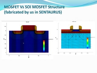
![Bulk Silicon and SOI MOSFET[2]
Bulk Silicon MOSFET &
Bulk Silicon wafer (cross section)
SOI MOSFET &
SOI wafer (cross section)](https://image.slidesharecdn.com/aa8e72c0-f6e3-495b-a898-b32d4772b0b8-160423091329/85/SOI-3-320.jpg)
![FLOW CHART[1]](https://image.slidesharecdn.com/aa8e72c0-f6e3-495b-a898-b32d4772b0b8-160423091329/85/SOI-4-320.jpg)
![SOI MOSFET STRUCTURE[2]](https://image.slidesharecdn.com/aa8e72c0-f6e3-495b-a898-b32d4772b0b8-160423091329/85/SOI-5-320.jpg)
![Disadvantage of SOI as Compared To
Conventional Silicon Substrate Device[1]
The primary barrier to SOI implementation is the
drastic increase in substrate cost, which
contributes an estimated 10–15% increase to total
manufacturing costs.
The buried oxide layer and concerns about
differential stress in the topmost silicon layer.](https://image.slidesharecdn.com/aa8e72c0-f6e3-495b-a898-b32d4772b0b8-160423091329/85/SOI-6-320.jpg)
![Different Manufacturing Methods of SOI[1]
Seed methods - wherein the topmost Si layer is grown directly on
the insulator. Seed methods require some sort of template for
homoepitaxy.
SIMOX - Separation by IMplantation of OXygen – uses an
oxygen ion beam implantation process followed by high temperature
annealing to create a buried SiO2 layer.
Wafer bonding – the insulating layer is formed by directly bonding
oxidized silicon with a second substrate.
One prominent example of a wafer bonding process is the Smart
Cut method
Nano Cleave that separates the silicon via stress at the interface
of silicon and silicon-germanium alloy.
ELTRAN is based on porous silicon and water cut.](https://image.slidesharecdn.com/aa8e72c0-f6e3-495b-a898-b32d4772b0b8-160423091329/85/SOI-7-320.jpg)
![Silicon-On-Insulator (SOI) Structures[2]
1. Silicon-On-Sapphire (SOS)
Low channel electron mobility is observed in SOS
MOSFETs ( ≈ 230-250 cm 2/V-sec)](https://image.slidesharecdn.com/aa8e72c0-f6e3-495b-a898-b32d4772b0b8-160423091329/85/SOI-8-320.jpg)
![2. Separation by Implanted Oxygen (SIMOX) Wafer Process[2]
Oxygen implant at:
-Energy 120-200 keV
-Dose ~0.3-1.8e18 cm-2
Anneal in inert ambient
above 1300°C, 3-6 hours
Multiple implants often reduce defect density
• Typical BOX thickness: 100, 200, 400 nm
• SOI film thickness varies from ~50 - 240 nm](https://image.slidesharecdn.com/aa8e72c0-f6e3-495b-a898-b32d4772b0b8-160423091329/85/SOI-9-320.jpg)
![3. Smart- Cut process[2]
Handle wafer B is bonded
Hydrogen implantation
through thermal oxide
dose ~1-5e16 cm-2
At ~400-600°C wafer
A separates from B
at H2 peak
After low temperature splitting, SOI wafer (B) is annealed ~1100°C to
strengthen the bond, whereas wafer A is reused. SOI film thickness
set by H2 implant energy and BOX thickness](https://image.slidesharecdn.com/aa8e72c0-f6e3-495b-a898-b32d4772b0b8-160423091329/85/SOI-10-320.jpg)
![Smart CUT Method[1]](https://image.slidesharecdn.com/aa8e72c0-f6e3-495b-a898-b32d4772b0b8-160423091329/85/SOI-11-320.jpg)
![4. ELTRAN Fabrication Process[2]](https://image.slidesharecdn.com/aa8e72c0-f6e3-495b-a898-b32d4772b0b8-160423091329/85/SOI-12-320.jpg)
![Benefits Of SOI Relative To Conventional
Silicon[1]
Lower parasitic capacitance due to isolation from the
bulk silicon, which improves power consumption at
matched performance.
Higher performance at equivalent VDD. Can work at
low VDD's.
Resistance to latch up due to complete isolation of
the n- and p-well structures.
Lower leakage currents due to isolation thus higher
power efficiency.
Reduced temperature dependency due to no doping.](https://image.slidesharecdn.com/aa8e72c0-f6e3-495b-a898-b32d4772b0b8-160423091329/85/SOI-13-320.jpg)
![SOI CMOS: Capacitance Advantage[2]
Junction capacitance: smaller than in bulk](https://image.slidesharecdn.com/aa8e72c0-f6e3-495b-a898-b32d4772b0b8-160423091329/85/SOI-14-320.jpg)
![SOI CMOS: Latch-up advantage[2]
Bulk CMOS SOI CMOS
latch-up free operation](https://image.slidesharecdn.com/aa8e72c0-f6e3-495b-a898-b32d4772b0b8-160423091329/85/SOI-15-320.jpg)
![Types of SOI Devices[1]
Partially Depleted SOI (PDSOI) Fully Depleted SOI (FDSOI)
For a n-type PDSOI MOSFET the
sandwiched p-type film between the
gate oxide (GOX) and buried oxide
(BOX) is large, so the depletion region
can't cover the whole p region. So to
some extent PDSOI behaves like bulk
MOSFET.
The film is very thin in FDSOI
devices so that the depletion region
covers the whole film. In FDSOI the
front gate (GOX) supports less
depletion charges than the bulk so
an increase in inversion charges
occurs resulting in higher switching
speeds.](https://image.slidesharecdn.com/aa8e72c0-f6e3-495b-a898-b32d4772b0b8-160423091329/85/SOI-16-320.jpg)
![Partially Depleted SOI MOSFET [2]
The basic device equations of PD SOI MOSFETs are the
same as for bulk devices, except of course from the
complications arising from the floating body (FBE)](https://image.slidesharecdn.com/aa8e72c0-f6e3-495b-a898-b32d4772b0b8-160423091329/85/SOI-17-320.jpg)
![Fully Depleted SOI MOSFET (thin SOI film )[2]
This electrostatic coupling, makes the front channel FD device
parameters dependent on the back gate voltage, including drain
current, threshold voltage, sub-threshold slope etc
In FDSOI case,
the front and
back channels are
electro-statically
coupled during
device operation](https://image.slidesharecdn.com/aa8e72c0-f6e3-495b-a898-b32d4772b0b8-160423091329/85/SOI-18-320.jpg)
![Relationship Between Threshold Voltage and
Capacitance[3]
Generally the threshold voltage (Vth) of the SOI
device can be expressed as follows:
V th =V FB +Q B /C OX,
where Vth represents a threshold voltage,
VFB represents a flat band voltage, QB represents
bulk charge, and COX represents capacitance of the
dielectric layer](https://image.slidesharecdn.com/aa8e72c0-f6e3-495b-a898-b32d4772b0b8-160423091329/85/SOI-19-320.jpg)
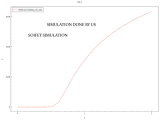
![SOIFET Characteristics[4]](https://image.slidesharecdn.com/aa8e72c0-f6e3-495b-a898-b32d4772b0b8-160423091329/85/SOI-22-320.jpg)
![Reference
[1] https://en.wikipedia.org/wiki/Silicon_on_insulator
[2] http://ece.iisc.ernet.in/~navakant/nano/2007/Lecture23.pdf
[3] https://www.google.com/patents/US6228691
[5] https://en.wikipedia.org/wiki/Silicon_on_sapphire
[6] https://en.wikipedia.org/wiki/Smart_cut
Research Papers
[4]
http://www.eecs.berkeley.edu/~hu/PUBLICATIONS/Hu_papers/Hu_
JNL/HuC_JNL_113.pdf
[4]
http://ieeexplore.ieee.org/stamp/stamp.jsp?tp=&arnumber=1626464
&tag=1](https://image.slidesharecdn.com/aa8e72c0-f6e3-495b-a898-b32d4772b0b8-160423091329/85/SOI-23-320.jpg)


This document discusses silicon on insulator (SOI) technology. It begins by defining SOI as using a layered silicon-insulator-silicon substrate instead of conventional silicon substrates in semiconductor manufacturing. It then explains the differences between bulk silicon MOSFETs and SOI MOSFETs. The document discusses several manufacturing methods for SOI, including SIMOX, wafer bonding, and Smart Cut. It also covers the benefits of SOI such as lower parasitic capacitance and resistance to latch-up. Finally, it distinguishes between partially depleted SOI and fully depleted SOI devices.


![workjnuuuuuuuuuuuooooooooooooooooooouuuuuuuuuuuuuuuuuuuuuuuuuu]]](https://cdn.slidesharecdn.com/ss_thumbnails/baippdtcblop01fie-251222045342-5aabffab-thumbnail.jpg?width=640&height=640&fit=bounds)


