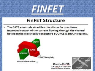
FINFET is a type of non-planar transistor with a conducting channel that is wrapped by a thin silicon fin. It was developed to overcome short channel effects seen in planar MOSFETs as transistors continue to shrink. Key aspects of FINFETs include the fin structure which allows gate control of the channel from both sides and the top, reducing leakage currents. Fabrication involves depositing fins and wrapping a gate material around them. FINFETs have been shown to effectively suppress short channel effects even at very small gate lengths, but come with increased manufacturing complexity and potential reliability issues compared to planar transistors.
In MOS, source-drain regions of adjacent MOS transistors together with interconnection metal lines may constitute parasitic MOS transistors unless they are isolated from each other. Hence, each MOSFET must be electrically isolated from each other. Device Isolation Techniques in VLSI microfabrication of MOS are discussed.
Multiple patterning is a class of technologies for manufacturing integrated circuits (ICs), developed for photolithography to enhance the feature density. The simplest case of multiple patterning is double patterning, where a conventional lithography process is enhanced to produce double the expected number of features. The resolution of a photoresist pattern is believed to blur at around 45 nm half-pitch. For the semiconductor industry, therefore, double patterning was introduced for the 32 nm half-pitch node and below. This presentation gives us an insight of why multiple patterning is an important to give us a better resolution below 32nm.
Securing your Kubernetes cluster_ a step-by-step guide to success !KatiaHIMEUR1
Today, after several years of existence, an extremely active community and an ultra-dynamic ecosystem, Kubernetes has established itself as the de facto standard in container orchestration. Thanks to a wide range of managed services, it has never been so easy to set up a ready-to-use Kubernetes cluster.
However, this ease of use means that the subject of security in Kubernetes is often left for later, or even neglected. This exposes companies to significant risks.
In this talk, I'll show you step-by-step how to secure your Kubernetes cluster for greater peace of mind and reliability.
Slack (or Teams) Automation for Bonterra Impact Management (fka Social Soluti...Jeffrey Haguewood
Sidekick Solutions uses Bonterra Impact Management (fka Social Solutions Apricot) and automation solutions to integrate data for business workflows.
We believe integration and automation are essential to user experience and the promise of efficient work through technology. Automation is the critical ingredient to realizing that full vision. We develop integration products and services for Bonterra Case Management software to support the deployment of automations for a variety of use cases.
This video focuses on the notifications, alerts, and approval requests using Slack for Bonterra Impact Management. The solutions covered in this webinar can also be deployed for Microsoft Teams.
Interested in deploying notification automations for Bonterra Impact Management? Contact us at sales@sidekicksolutionsllc.com to discuss next steps.
The Art of the Pitch: WordPress Relationships and SalesLaura Byrne
Clients don’t know what they don’t know. What web solutions are right for them? How does WordPress come into the picture? How do you make sure you understand scope and timeline? What do you do if sometime changes?
All these questions and more will be explored as we talk about matching clients’ needs with what your agency offers without pulling teeth or pulling your hair out. Practical tips, and strategies for successful relationship building that leads to closing the deal.
Neuro-symbolic is not enough, we need neuro-*semantic*Frank van Harmelen
Neuro-symbolic (NeSy) AI is on the rise. However, simply machine learning on just any symbolic structure is not sufficient to really harvest the gains of NeSy. These will only be gained when the symbolic structures have an actual semantics. I give an operational definition of semantics as “predictable inference”.
All of this illustrated with link prediction over knowledge graphs, but the argument is general.
State of ICS and IoT Cyber Threat Landscape Report 2024 previewPrayukth K V
The IoT and OT threat landscape report has been prepared by the Threat Research Team at Sectrio using data from Sectrio, cyber threat intelligence farming facilities spread across over 85 cities around the world. In addition, Sectrio also runs AI-based advanced threat and payload engagement facilities that serve as sinks to attract and engage sophisticated threat actors, and newer malware including new variants and latent threats that are at an earlier stage of development.
The latest edition of the OT/ICS and IoT security Threat Landscape Report 2024 also covers:
State of global ICS asset and network exposure
Sectoral targets and attacks as well as the cost of ransom
Global APT activity, AI usage, actor and tactic profiles, and implications
Rise in volumes of AI-powered cyberattacks
Major cyber events in 2024
Malware and malicious payload trends
Cyberattack types and targets
Vulnerability exploit attempts on CVEs
Attacks on counties – USA
Expansion of bot farms – how, where, and why
In-depth analysis of the cyber threat landscape across North America, South America, Europe, APAC, and the Middle East
Why are attacks on smart factories rising?
Cyber risk predictions
Axis of attacks – Europe
Systemic attacks in the Middle East
Download the full report from here:
https://sectrio.com/resources/ot-threat-landscape-reports/sectrio-releases-ot-ics-and-iot-security-threat-landscape-report-2024/
JMeter webinar - integration with InfluxDB and GrafanaRTTS
Watch this recorded webinar about real-time monitoring of application performance. See how to integrate Apache JMeter, the open-source leader in performance testing, with InfluxDB, the open-source time-series database, and Grafana, the open-source analytics and visualization application.
In this webinar, we will review the benefits of leveraging InfluxDB and Grafana when executing load tests and demonstrate how these tools are used to visualize performance metrics.
Length: 30 minutes
Session Overview
-------------------------------------------
During this webinar, we will cover the following topics while demonstrating the integrations of JMeter, InfluxDB and Grafana:
- What out-of-the-box solutions are available for real-time monitoring JMeter tests?
- What are the benefits of integrating InfluxDB and Grafana into the load testing stack?
- Which features are provided by Grafana?
- Demonstration of InfluxDB and Grafana using a practice web application
To view the webinar recording, go to:
https://www.rttsweb.com/jmeter-integration-webinar
Epistemic Interaction - tuning interfaces to provide information for AI supportAlan Dix
Paper presented at SYNERGY workshop at AVI 2024, Genoa, Italy. 3rd June 2024
https://alandix.com/academic/papers/synergy2024-epistemic/
As machine learning integrates deeper into human-computer interactions, the concept of epistemic interaction emerges, aiming to refine these interactions to enhance system adaptability. This approach encourages minor, intentional adjustments in user behaviour to enrich the data available for system learning. This paper introduces epistemic interaction within the context of human-system communication, illustrating how deliberate interaction design can improve system understanding and adaptation. Through concrete examples, we demonstrate the potential of epistemic interaction to significantly advance human-computer interaction by leveraging intuitive human communication strategies to inform system design and functionality, offering a novel pathway for enriching user-system engagements.
Key Trends Shaping the Future of Infrastructure.pdfCheryl Hung
Keynote at DIGIT West Expo, Glasgow on 29 May 2024.
Cheryl Hung, ochery.com
Sr Director, Infrastructure Ecosystem, Arm.
The key trends across hardware, cloud and open-source; exploring how these areas are likely to mature and develop over the short and long-term, and then considering how organisations can position themselves to adapt and thrive.
Kubernetes & AI - Beauty and the Beast !?! @KCD Istanbul 2024Tobias Schneck
As AI technology is pushing into IT I was wondering myself, as an “infrastructure container kubernetes guy”, how get this fancy AI technology get managed from an infrastructure operational view? Is it possible to apply our lovely cloud native principals as well? What benefit’s both technologies could bring to each other?
Let me take this questions and provide you a short journey through existing deployment models and use cases for AI software. On practical examples, we discuss what cloud/on-premise strategy we may need for applying it to our own infrastructure to get it to work from an enterprise perspective. I want to give an overview about infrastructure requirements and technologies, what could be beneficial or limiting your AI use cases in an enterprise environment. An interactive Demo will give you some insides, what approaches I got already working for real.
UiPath Test Automation using UiPath Test Suite series, part 3DianaGray10
Welcome to UiPath Test Automation using UiPath Test Suite series part 3. In this session, we will cover desktop automation along with UI automation.
Topics covered:
UI automation Introduction,
UI automation Sample
Desktop automation flow
Pradeep Chinnala, Senior Consultant Automation Developer @WonderBotz and UiPath MVP
Deepak Rai, Automation Practice Lead, Boundaryless Group and UiPath MVP
Accelerate your Kubernetes clusters with Varnish CachingThijs Feryn
A presentation about the usage and availability of Varnish on Kubernetes. This talk explores the capabilities of Varnish caching and shows how to use the Varnish Helm chart to deploy it to Kubernetes.
This presentation was delivered at K8SUG Singapore. See https://feryn.eu/presentations/accelerate-your-kubernetes-clusters-with-varnish-caching-k8sug-singapore-28-2024 for more details.
2. INTRODUCTION TO FINFET
• The term “FINFET” describes a nonplanar, double gate transistor built on an SOI
substrate, based on the single gate transistor
design.
• The important characteristics of FINFET is that
the conducting channel is wrapped by a thin Si
“fin”, which forms the body of the device.
• The thickness of the fin determines the
effective channel length of the device.
3. HISTORY OF FINFET
• FINFET is a transistor design first developed by
Chenming Hu and his colleagues at the
University of California at Berkeley, which tries
to overcome the worst types of SCE(Short
Channel Effect).
• Originally, FINFET was developed for use on
Silicon-On-Insulator(SOI).
• SOI FINFET with thick oxide on top of fin are
called “Double-Gate” and those with thin
oxide on top as well as on sides are called
“Triple-Gate” FINFETs
4. REASON FOR EVOLUTION OF
FINFET
• For the double gate SOI MOSFETs, the gates
control the energy barrier b/w source and
drain effectively.
• Therefore, the Short Channel Effect(SCE) can
be suppressed without increasing the
channel impurity concentration.
5. GENERAL LAYOUT & MODE OF
OPERATION
• The basic electrical layout and mode of
operation of a FINFET does not differ from a
traditional FET.
• There is one source and one drain contact as
well as a gate to control the current flow.
• In contrast to planar MOSFET, the channel b/w
source and drain is build as 3D bar on top of
the Si substrate and are called fin.
6. CONTINUED………
The gate electrode is then wrapped around the channel, so that
there can be formed several gate electrodes on each side which
leads to the reduction in the leakage currents and an enhanced
drive current.
7. “FINS”
• The fin is used to form the raised channel.
• As the channel is very thin the gate has a great
control over carriers within it, but, when the
device is switched on, the shape limits the
current through it to a low level.
• The thickness of the fin (measured in the
direction from source to drain) determines the
effective length of the device.
8. FABRICATION OF FINFET
• The heart of the FINFET is a thin Si fin, which
serves as a body of the MOSFET.
• A heavily doped poly Si film wraps around the
fin and makes the electrical contact to the
vertical faces of the fin.
• A gap is etched through the poly Si film to
separate the source and drain.
The various steps in the fabrication of FINFETs
are discussed as follows.
9. CHEMICAL VAPOUR DEPOSITION(CVD)
• SiN and SiO layers are deposited on Si film to
make a hard mask or a cover layer.
• The cover layer will protect the Si fin
throughout the fabrication process.
• Then, a layer of SiO2 is developed by the
process of dry etching.
• The layer of SiO2 is used to relieve the stress.
10. ELECTRON BEAM LITHOGRAPHY
• The fine Si fin is patterned by EB Lithography
with 100keV acceleration energy.
• The resist pattern is slightly ashed at 5W and
30 sec to reduce the Si fin width.
• Then using top SiO layer as a hard etching
mask, the SiO layer is etched.
• By this process, the silicon fin is patterned.
11. NEXT PROCESSES
• A thin layer of sacrificial layer of SiO2 is grown.
• Then, the sacrificial oxide is stripped completely
to remove etch damage.
• While the cover layer protects the Si fin, the
amorphous Si is completely removed from the
side of the Si fin.
• The amorphous Si is in contact with the Si fin at
its side surfaces becomes the impurity diffusion
source that forms the transistor source and drain.
12. OXIDATION
• The gate oxidation should thin the Si fin width
slightly.
• By oxidizing the Si surface, gate oxide as thin
as 2.5nm is grown.
• Because the area of Si fin inside the surface is
too small, we use dummy wafers to measure
the oxide thickness.
• Hence the gate oxide is grown.
13. FORMATION OF POLY-Si GATE
• The boron doped Si is deposited at 475`C as
the gate material.
• Because the source and drain extension is
already formed and covered by thick SiO
layer, no high temperature steps are required
after the gate deposition.
• The total parasitic resistance due to probing is
about 3000.
14. HOW TO REDUCE COMPLEXITY OF
FABRICATION???
– Due to the complexity of fabrication process, the
FINFET design was proposed to have a delta
structure, so that after the reduction of vertical
feature height, the gate channel-Gate stacked
structure is realized by a Quasi-Planar technology.
16. REASON FOR POOR PERFORMANCE:
• Large bits and holes in the Si fin and the
source drain areas.
• In fabrication, photo resist alone is not a
sufficient task.
17. PARASITIC CAPACITANCE
• It is also known as stray capacitance.
• In electrical circuits, Parasitic capacitance is an
unavoidable and usually wanted capacitance
that exists b/w parts of an electronic
component or circuit simply because of their
proximity (relationship) to each other.
• Circuit elements such as inductors, diodes and
transistors have internal capacitance and
derivate from the circuit elements.
18. HOW TO AVOID PARASITIC
CAPACITANCE
• Additional process steps are required to
induce impurities (appropriate type) below
the fin to provide a Punch-Through
Stop(PTS), ensuring there is no direct current
path b/w gate and source and are electrically
controlled by gate input.
19. SHORT CHANNEL EFFECT
• It is an effect whereby a MOSFET in which the
channel length is the same order of
magnitude as the depletion layer widths of
source & drain junctions, behaves differently
from the other MOSFETs.
• As the channel length ‘l’ is reduced to increase
both the operation speed and the number of
components per chip, the so called SCE
occurs.
20. ATTRIBUTES OF THE SHORT CHANNEL
EFFECT
1. Limitation imposed on the electron drift
characteristics in the channel.
2. Modification of threshold voltage (Short
Channel Effect(SCE))
22. ADVANTAGES OF FINFET
• Higher technological maturity than planar DG.
• Suppressed Short Channel Effect(SCE)
• Better in driving current
• More compact
• Low cost
23. DISADVANTAGES OF FINFET
• Reduced mobility for electrons
• Higher source and drain resistances
• Poor reliability
24. LATEST UPDATES ABOUT FINFET
• In the New York Times, On may 4 2011, it was
published that INTEL will use FINFET for about
22nm.
• According to various sources, INTEL’s FINFET
shape has an unusual shape of a triangle
rather than rectangle because triangle has a
high structural strength, higher area to volume
ratio thus increasing the switching
performance.
25. CONCLUSION
The following key features are
experimentally verified.
• The self aligned double gate effectively
suppresses Short Channel Effect even in 17nm
gate length.
• Gate is self-aligned, which is raised to reduce
the parasitic capacitance.