Download as PDF, PPTX


![Let
C1/ C2 = 3.4 = 2+1.4
= [6/3] + [1.4/1][6/3] [1.4/1]
[6/3]---can be implemented by using unit[6/3]---can be implemented by using unit
capacitors
[1 4/1]---we require non unit capacitor[1.4/1]---we require non unit capacitor
Mismatch can occur due to second term
BITS Pilani, Pilani Campus](https://image.slidesharecdn.com/aicdcmoslayouts-130903111747-/75/Aicd-cmos-layouts-32-2048.jpg)


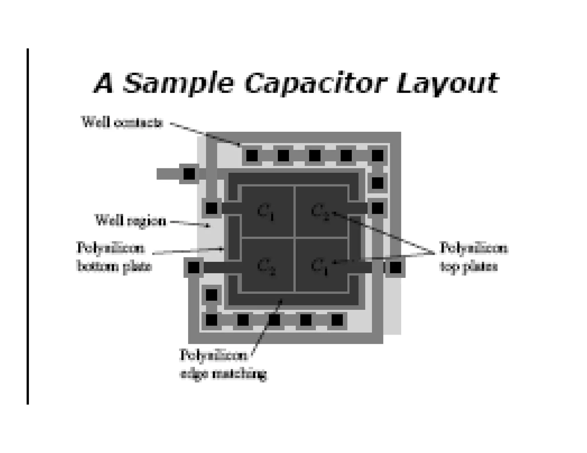


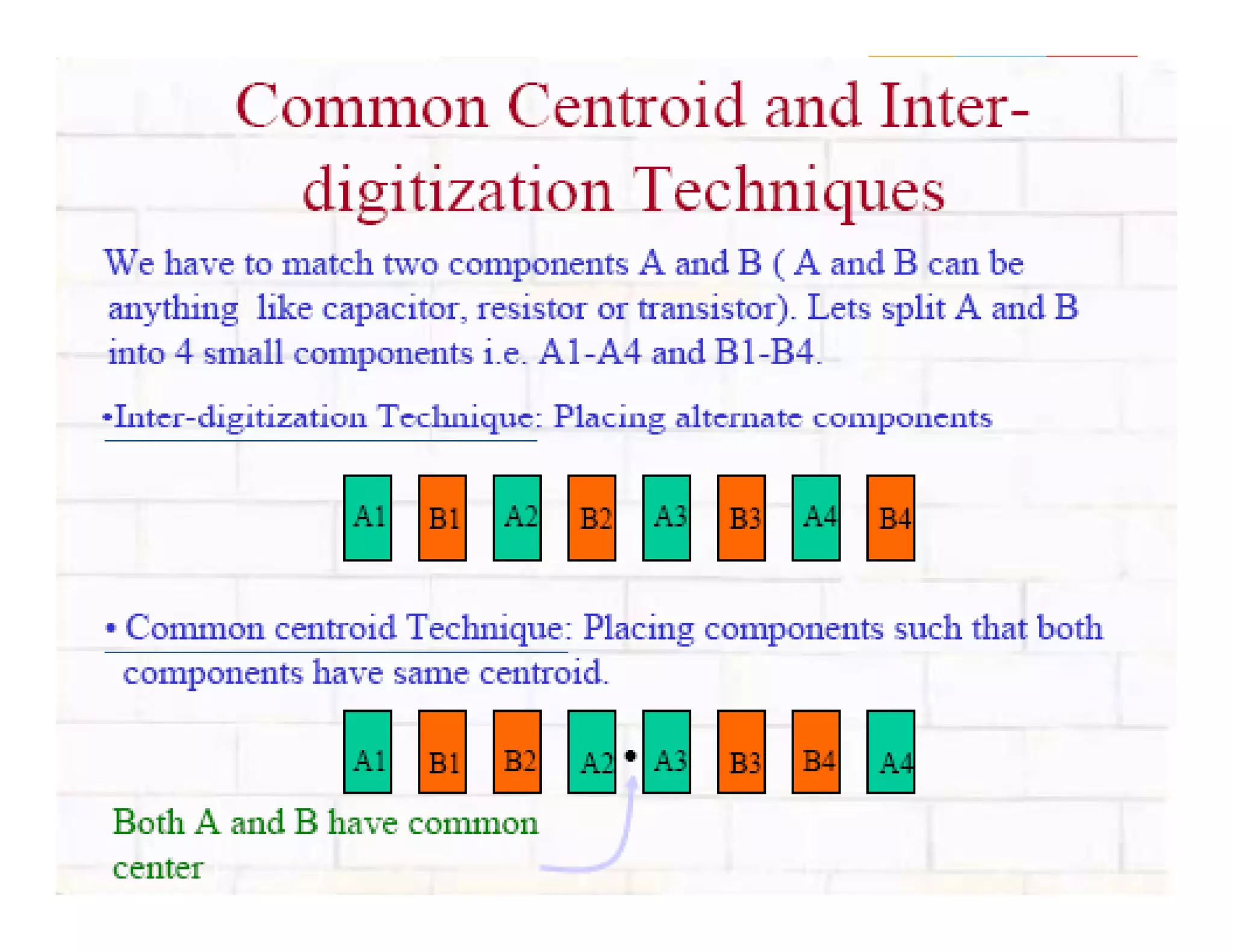


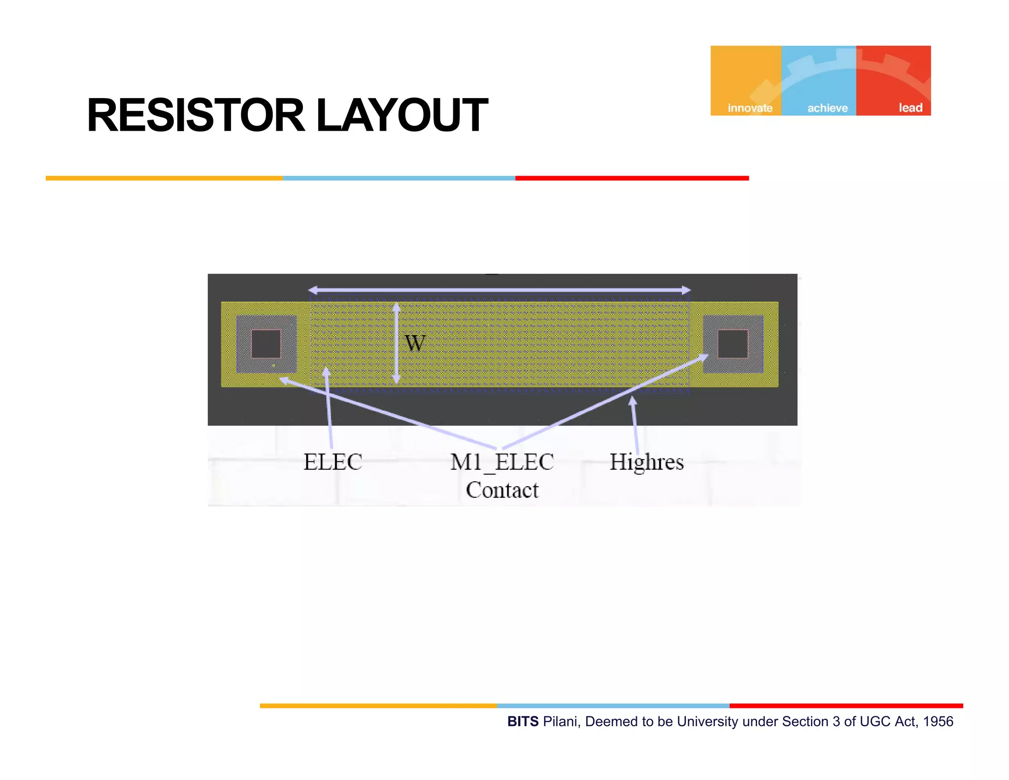
This document discusses analog integrated circuit layout techniques. It covers topics like design rules, unit component design, boundary condition matching using common centroid layout, and reducing mismatches. Specific circuit elements discussed include MOS transistors, capacitors, and resistors. Layout techniques to reduce parasitic capacitances and handle over-etching errors are presented. Fingered device layouts and calculating parasitic capacitances of MOS devices are also summarized.