Downloaded 364 times


![Thapar University , PatialaSunday, March 12, 2017 3
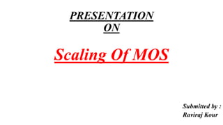
Moore’s Law[1]
No. of transistors on a chip doubled every 18 to 24 months.
Semiconductor technology will double its effectiveness every 18 months.
Fig. 1 : No. of transistors with years](https://image.slidesharecdn.com/presentation-copy-170312125047/85/Presentation-on-Scaling-3-320.jpg)
![Why Scaling?[2]
Thapar University , PatialaSunday, March 12, 2017 6
Design of high density chips in MOS VLSI technology requires:
High packing density of MOSFETS
Small transistor size
This reduction of size is k/a Scaling.
S>1 has been introduced leading to reduction of area by a factor S².
Disadvantage : Electric fields within the Gate Oxide grow larger.](https://image.slidesharecdn.com/presentation-copy-170312125047/85/Presentation-on-Scaling-6-320.jpg)
![Statistics[3]
Thapar University , PatialaSunday, March 12, 2017 7
Fig. 4 : Data showing no. of transistors on processors of Intel Corporation
with Years](https://image.slidesharecdn.com/presentation-copy-170312125047/85/Presentation-on-Scaling-7-320.jpg)

![Thapar University , PatialaSunday, March 12, 2017 14
When channel length Leff approx. equals source and junction depth xj.
Why Short Channel MOS , even if it has degraded performance ?
Threshold voltage is less. Why ?
Effects :
Drain- Induced Barrier Lowering
Surface Scattering
Velocity Saturation
Impact Ionization
Hot Carrier Effect
Short Channel Effects[4]](https://image.slidesharecdn.com/presentation-copy-170312125047/85/Presentation-on-Scaling-14-320.jpg)
![ Potential barrier is controlled by both VGS and VDS.
If drain voltage increases , barrier in the channel decreases , leading to DIBL.
Allows electron flow between S and D even at VGS < VTO .
A. Drain- Induced Barrier Lowering (DIBL)[5]
Fig. 10 : As channel length decreases, the barrier φB to be surmounted by an electron,
from the source on its way to the drain reduces.
Thapar University , PatialaSunday, March 12, 2017 16](https://image.slidesharecdn.com/presentation-copy-170312125047/85/Presentation-on-Scaling-16-320.jpg)
![Thapar University , PatialaSunday, March 12, 2017 17
B. Surface Scattering
Due to SCE , electric field increases and mobility becomes field dependent.
Surface scattering occurs.
Average surface mobility decreases.
Fig. 11: Pictorial representation of Surface Scattering[6]](https://image.slidesharecdn.com/presentation-copy-170312125047/85/Presentation-on-Scaling-17-320.jpg)
![Thapar University , PatialaSunday, March 12, 2017 20
D. Impact Ionisation[7]
Due to high electric field which causes high velocity of electrons.
Generates Electron - Hole pairs.
Fig. 15 : Impact Ionization](https://image.slidesharecdn.com/presentation-copy-170312125047/85/Presentation-on-Scaling-20-320.jpg)
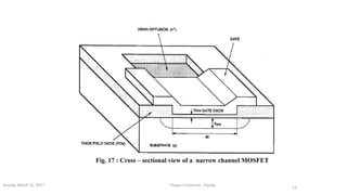
![Narrow Channel Effects[8]
MOS having channel widths (W) approx. equals depletion region
thickness (xdm) is known as Narrow – Channel MOS.
Here , Vto (narrow channel) = Vto + ΔVto (most significant)
Overlapping of Gate Oxide and FOX.
Thapar University , PatialaSunday, March 12, 2017
22](https://image.slidesharecdn.com/presentation-copy-170312125047/85/Presentation-on-Scaling-22-320.jpg)

![References
[1] lect15-scaling.ppt
[2] Cmos Digital Integrated Circuits - Sung-Mo Kang and Yusuf Leblebici.pdf , pg. no. 115 ,
TATA MCGRAW – HILL EDITION
[3] www.intel.com/research/silicon/mooreslaw.htm
[4] Cmos Digital Integrated Circuits - Sung-Mo Kang and Yusuf Leblebici.pdf , pg. no. 119 ,
TATA MCGRAW – HILL EDITION
[5] Cmos Digital Integrated Circuits - Sung-Mo Kang and Yusuf Leblebici.pdf , pg. no. 127 ,
TATA MCGRAW – HILL EDITION
[6] EE327 Lec 30a - Surface scattering
[7] Introduction to VLSI design (EECS 467) Project Short-Channel Effects in MOSFETs
December 11th, 2000 Fabio D’Agostino Daniele Quercia pdf , pg. no. 3.
[8] Cmos Digital Integrated Circuits - Sung-Mo Kang and Yusuf Leblebici.pdf , page no. 125 ,
TATA MCGRAW – HILL EDITION
Sunday, March 12, 2017 Thapar University , Patiala 25](https://image.slidesharecdn.com/presentation-copy-170312125047/85/Presentation-on-Scaling-25-320.jpg)

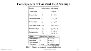
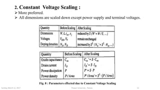
This presentation discusses MOSFET scaling and its challenges. It begins by covering Moore's Law, which states that the number of transistors on a chip doubles every 18 months. As sizes shrink due to scaling, short channel effects like drain-induced barrier lowering and hot carrier effects emerge. The presentation covers two types of scaling: constant field scaling, which keeps electric fields constant but increases power density; and constant voltage scaling, which is preferred as it avoids increased power density but reduces threshold voltage. Narrow width effects also occur when channel widths shrink and depletion regions overlap. Overall, the presentation provides an overview of MOSFET scaling techniques and the short channel effects that emerge as sizes shrink.


