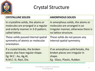
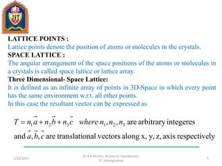
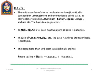
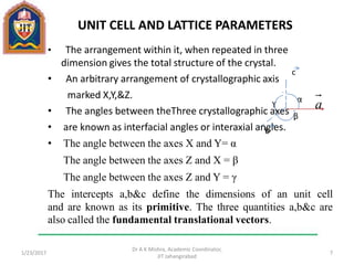
Downloaded 106 times

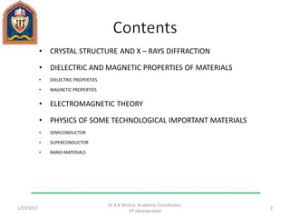
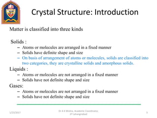
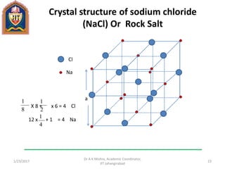
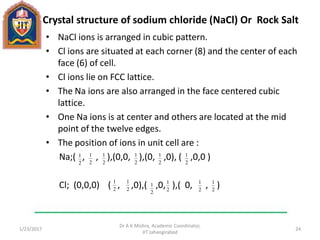
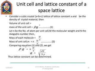
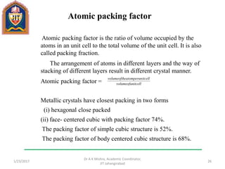
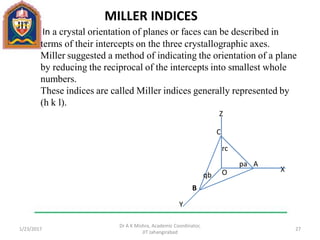

This document contains notes from a lecture on crystal structure and X-ray diffraction taught by Dr. A K Mishra. It discusses the classification of solids as crystalline or amorphous, lattice structures including simple cubic, body centered cubic and face centered cubic, basis, unit cell, Bravais lattices, coordination numbers, atomic packing factors and examples including the crystal structure of sodium chloride. The notes also describe how to calculate atomic radius and lattice constants from structural parameters.