Download as PDF, PPTX
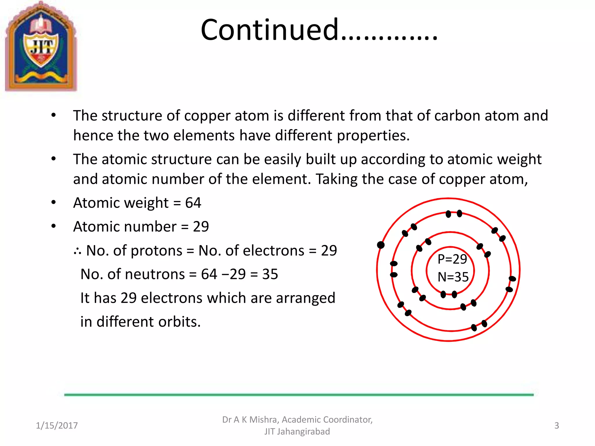
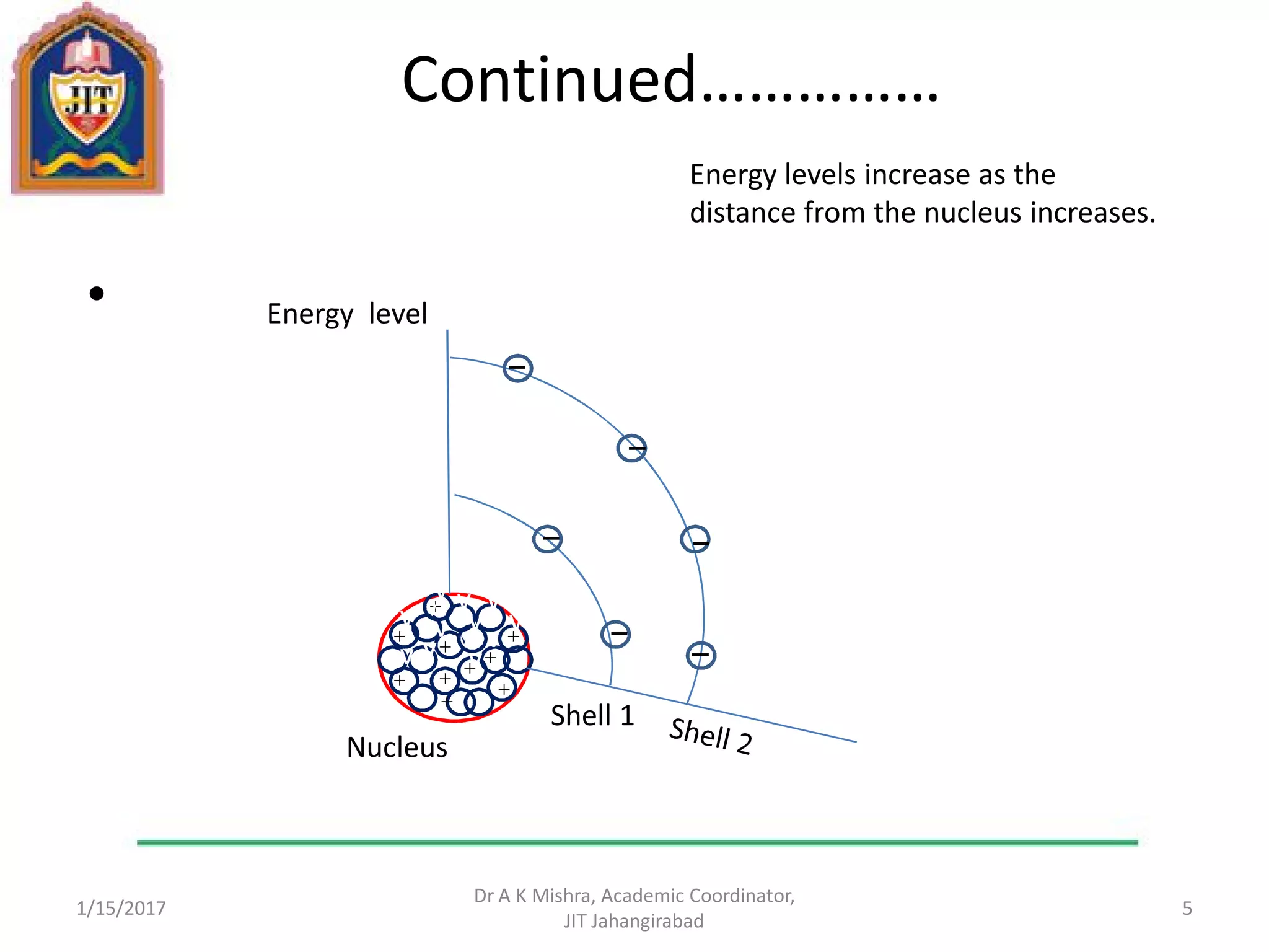
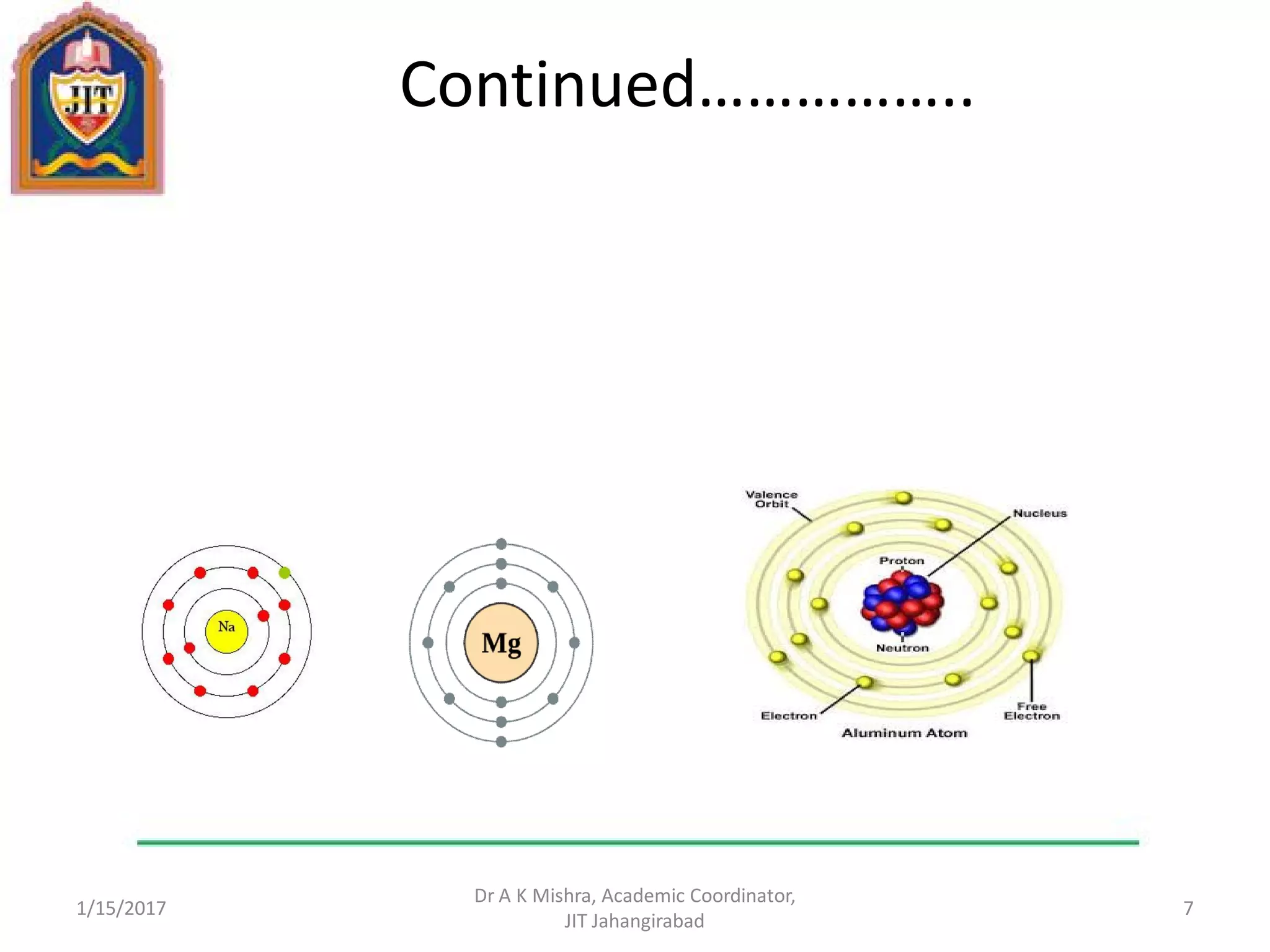
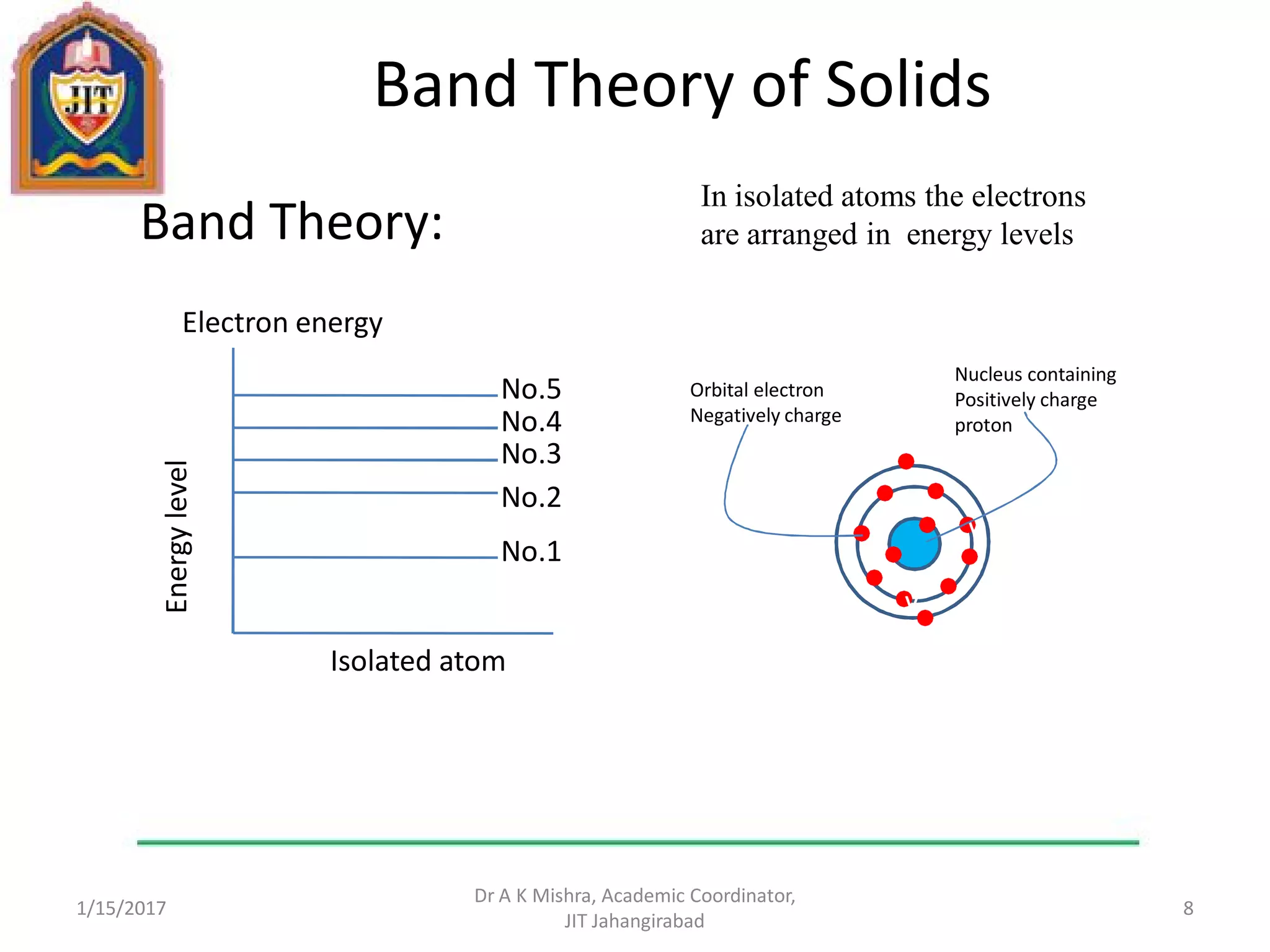
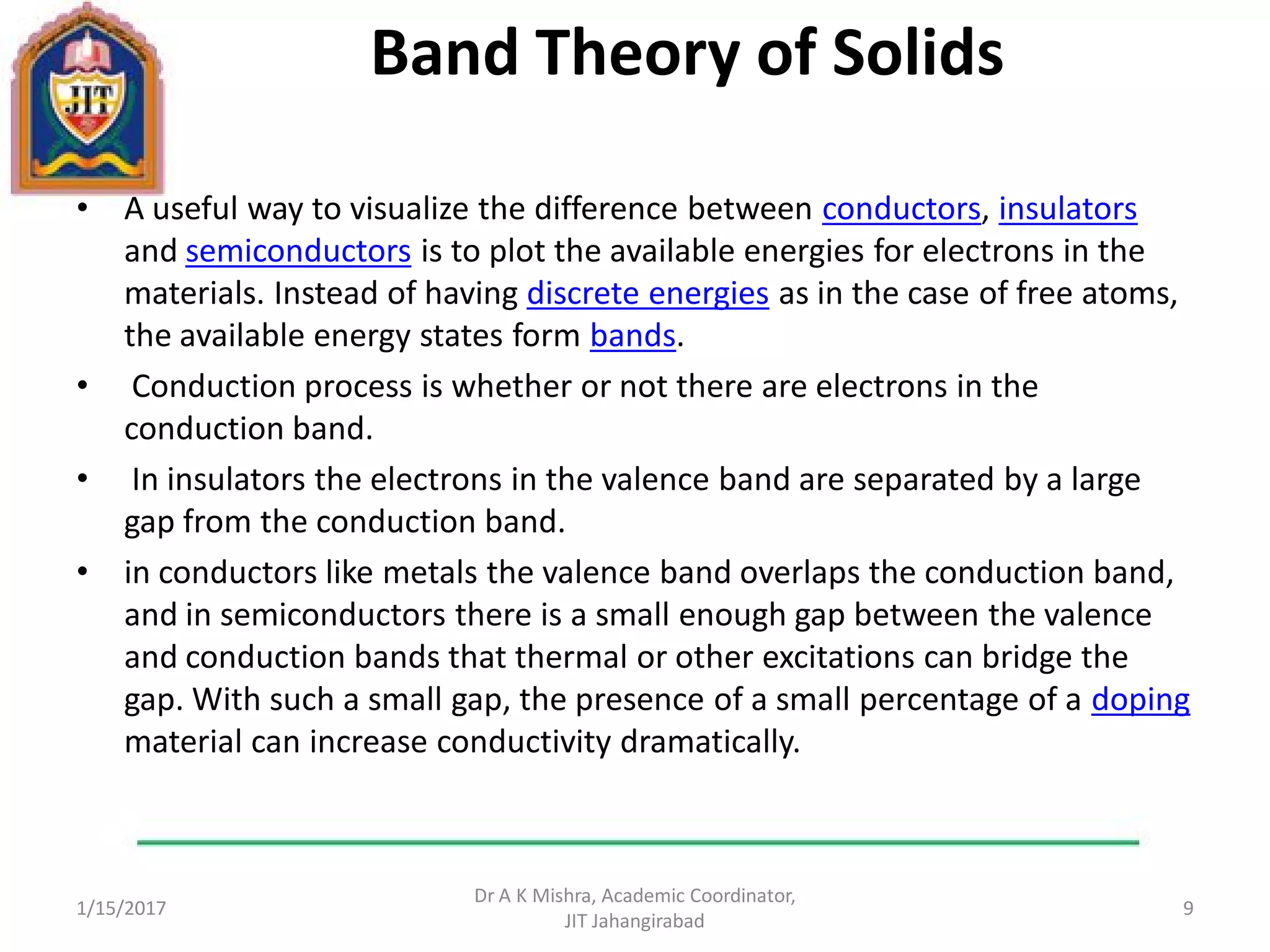
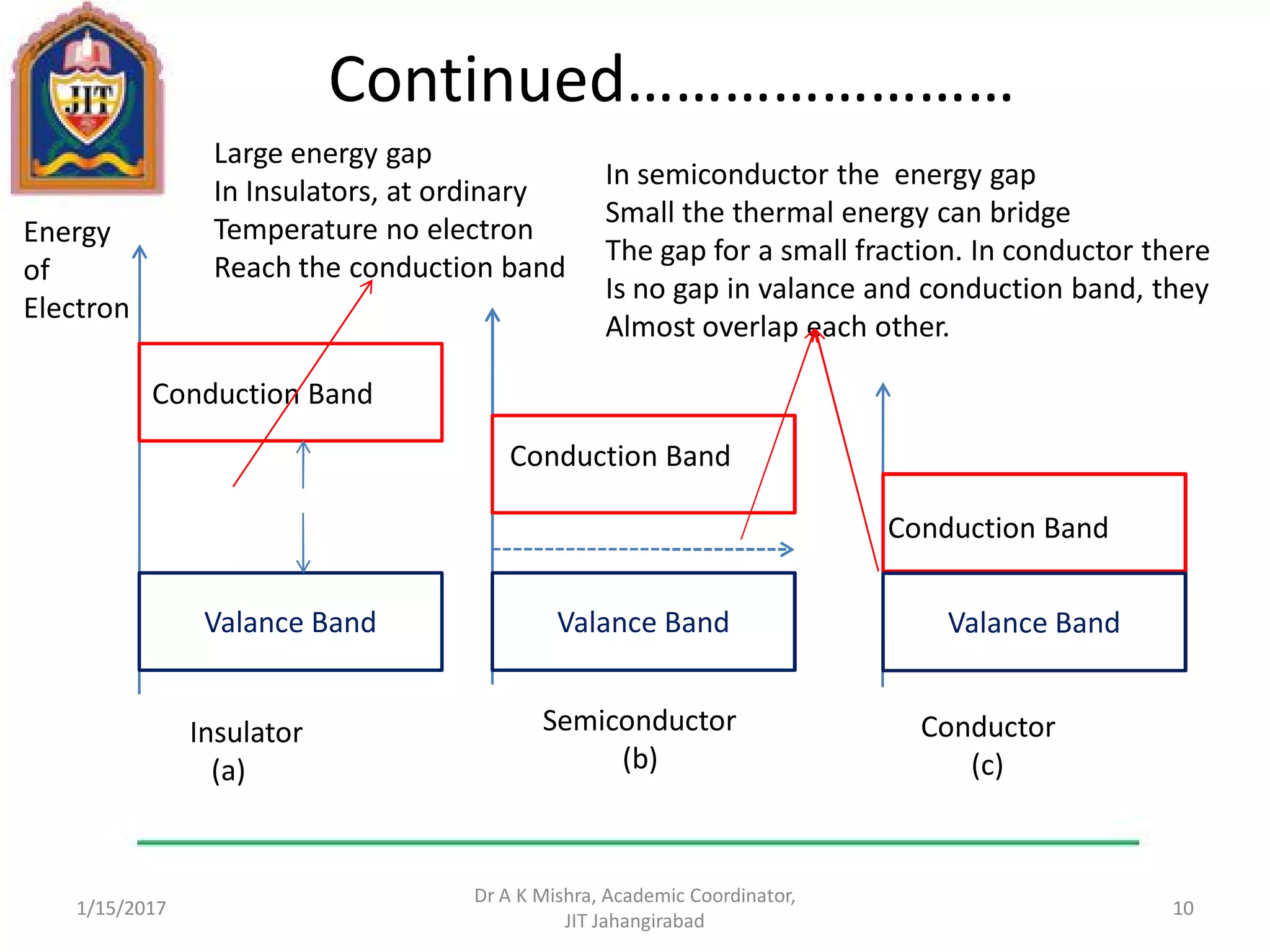
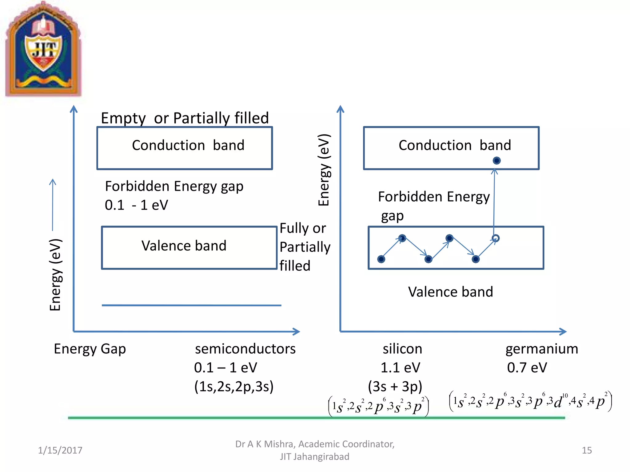

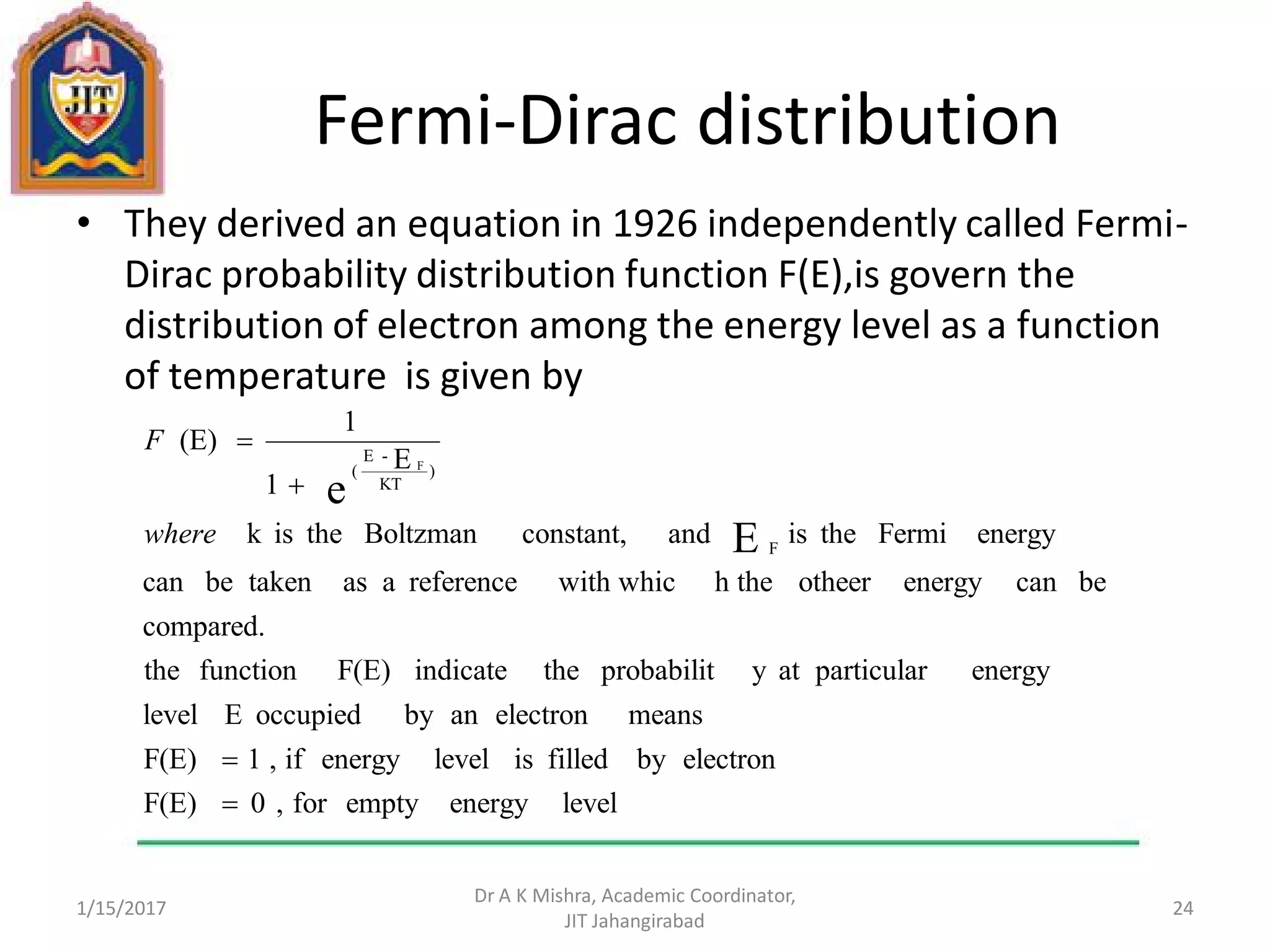
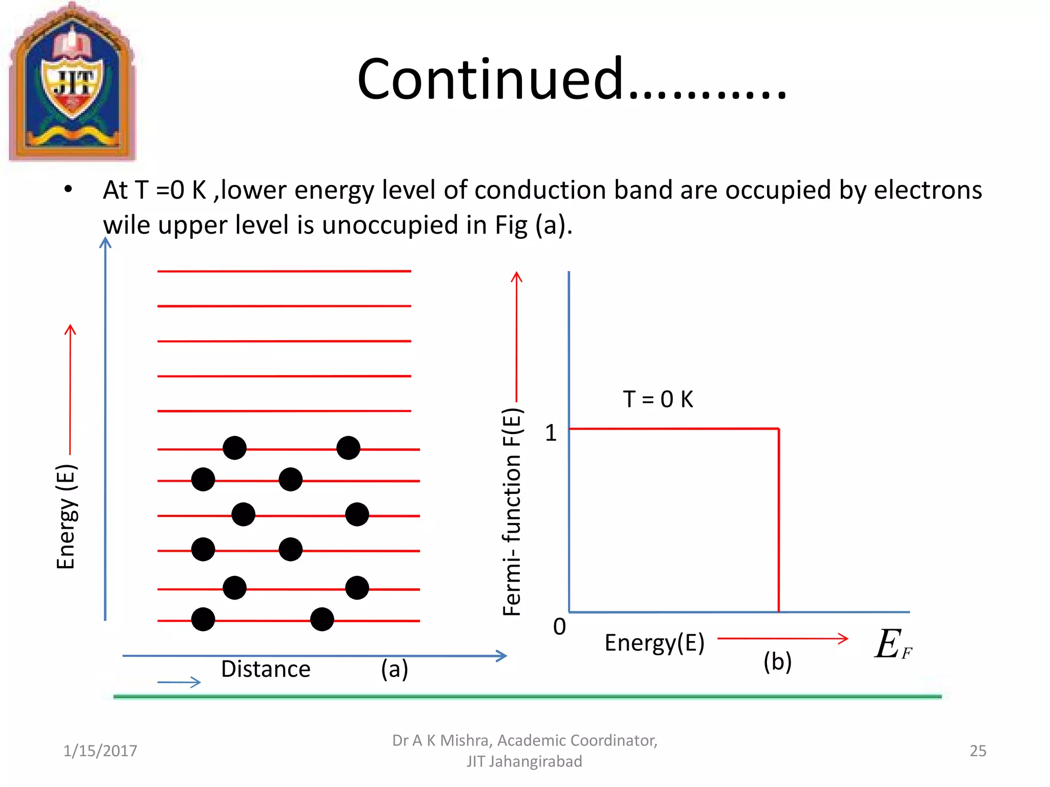
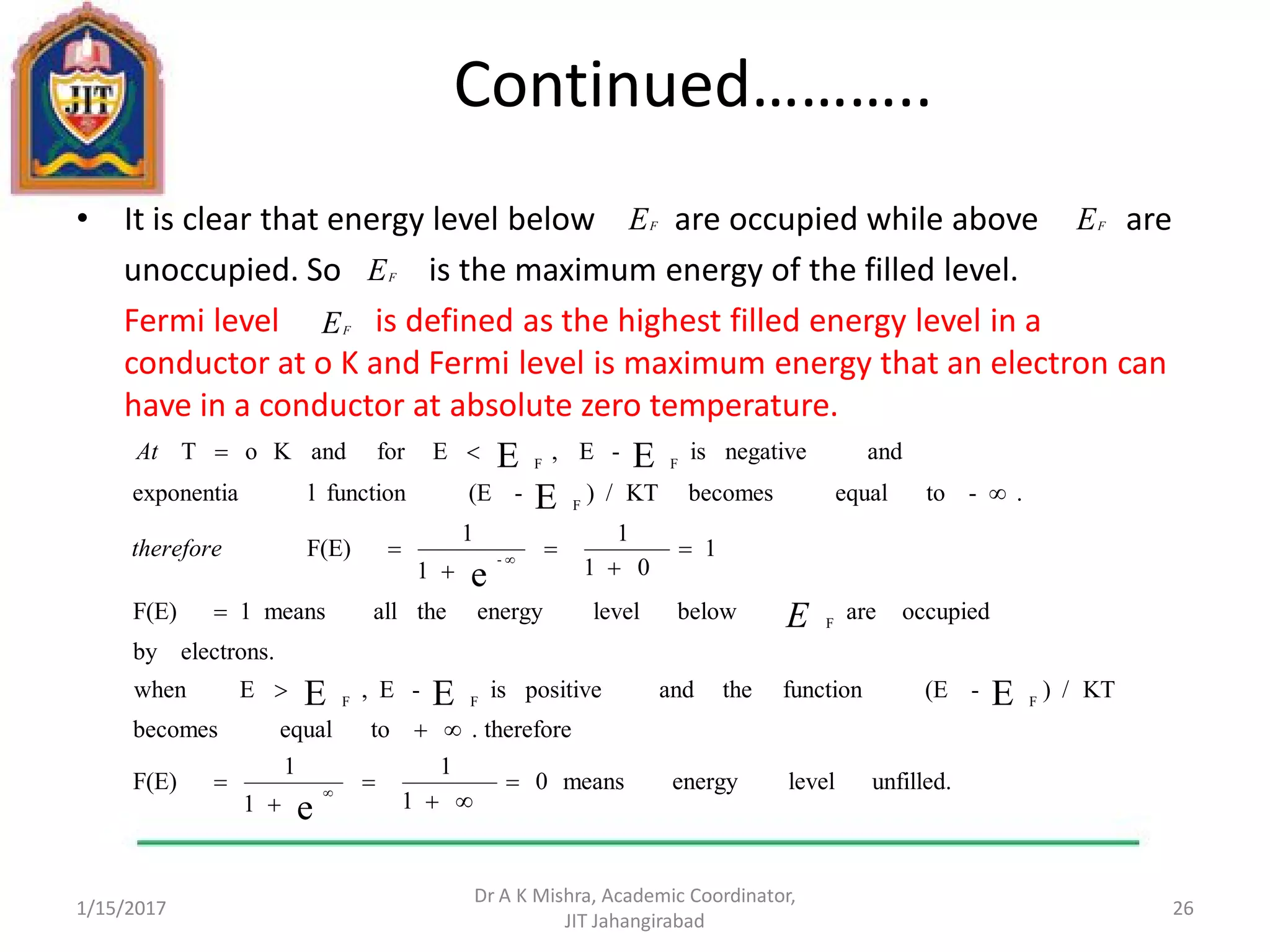
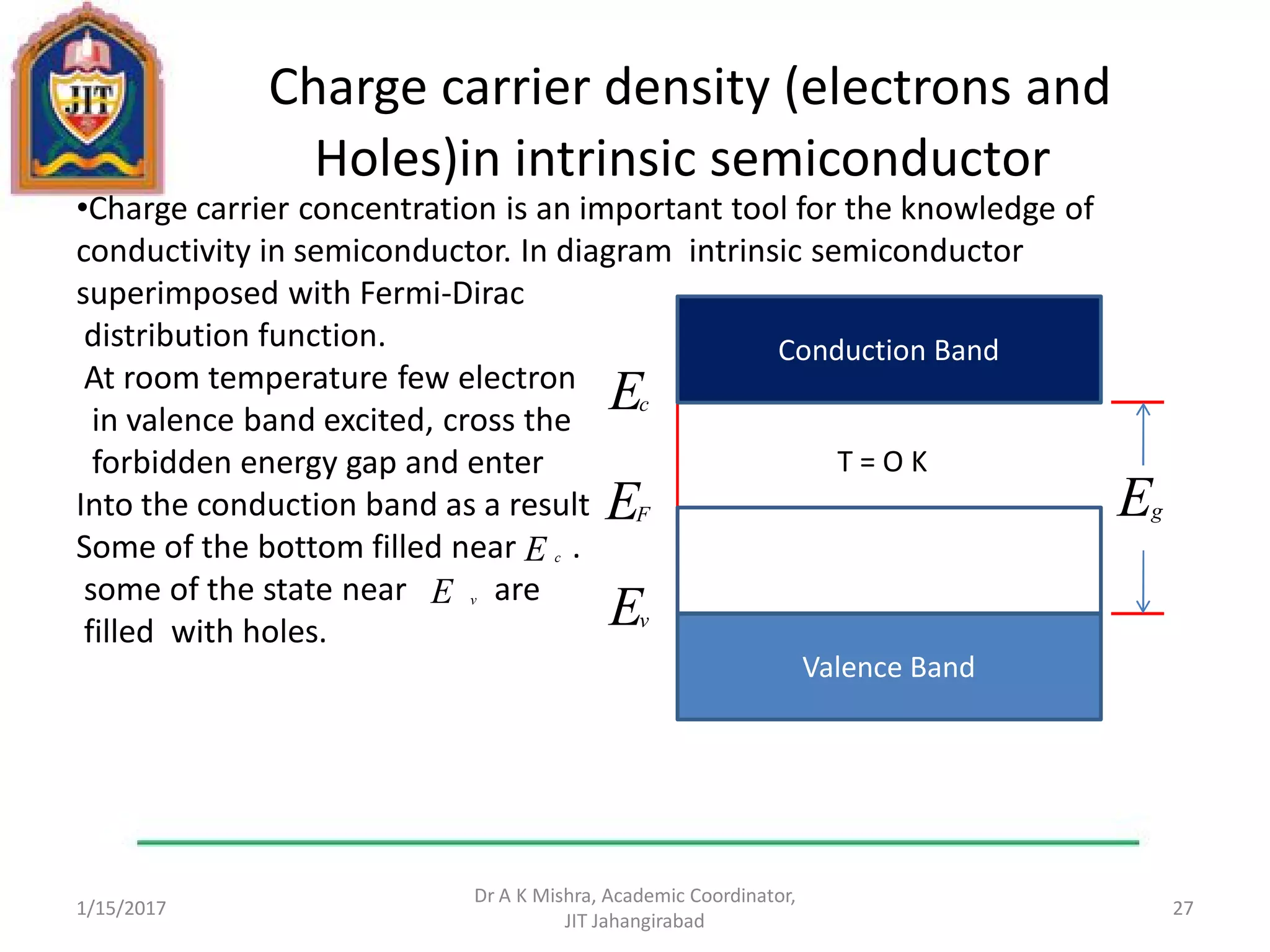
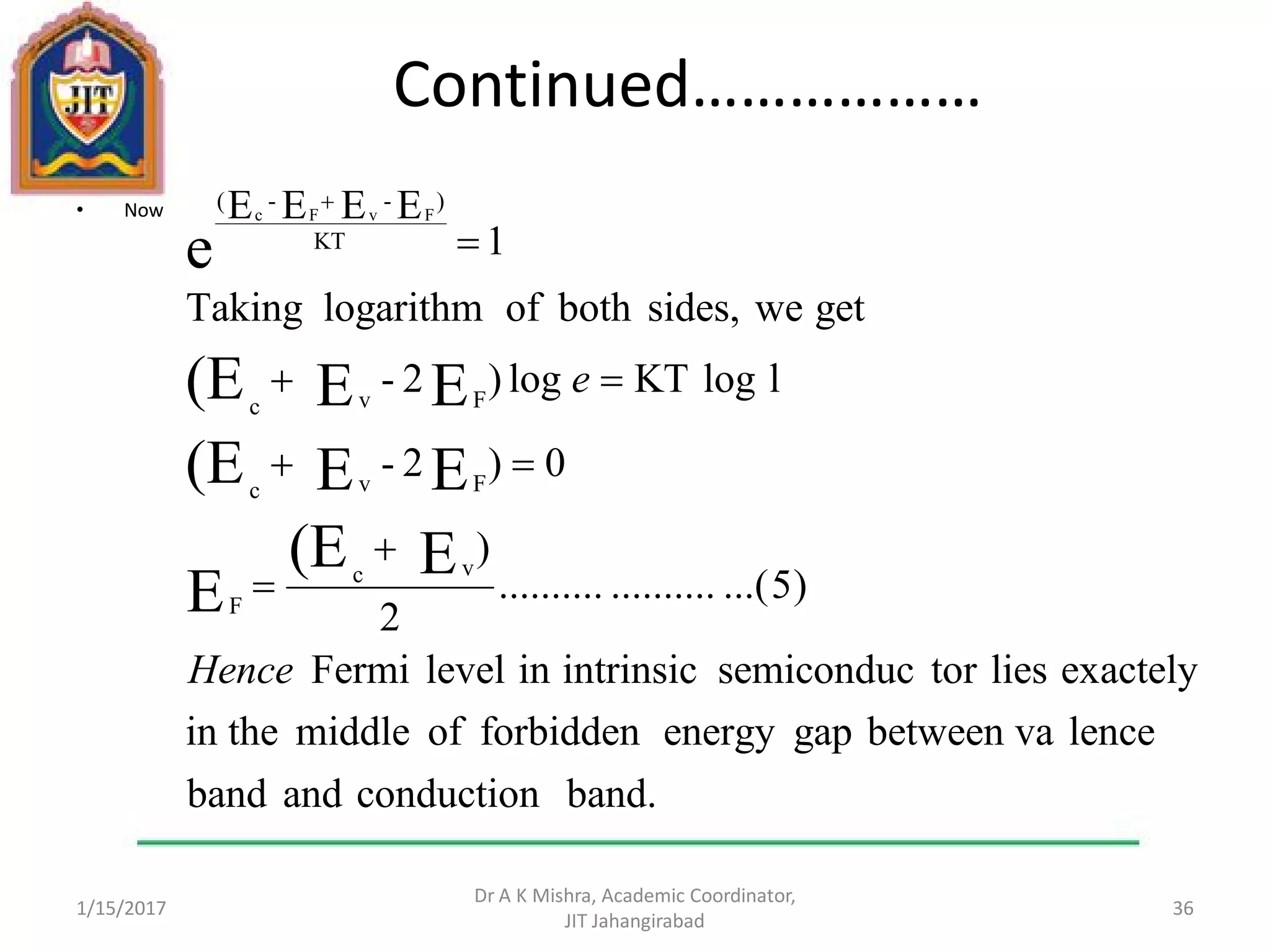
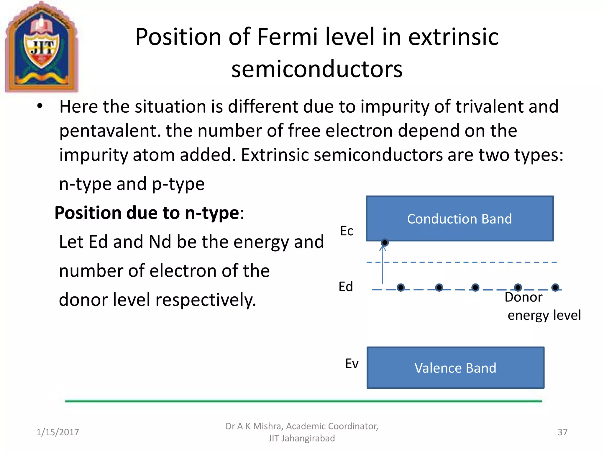
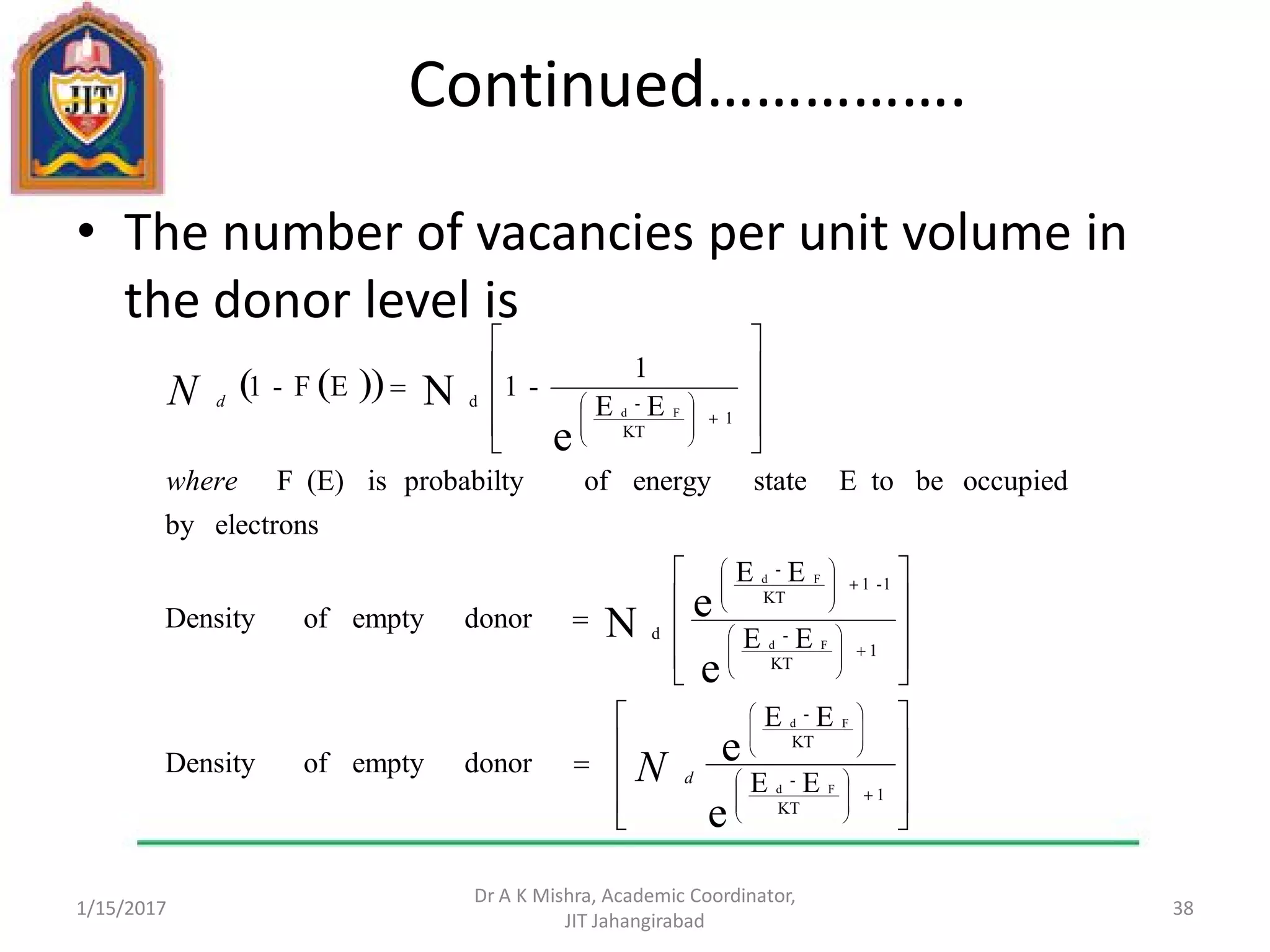
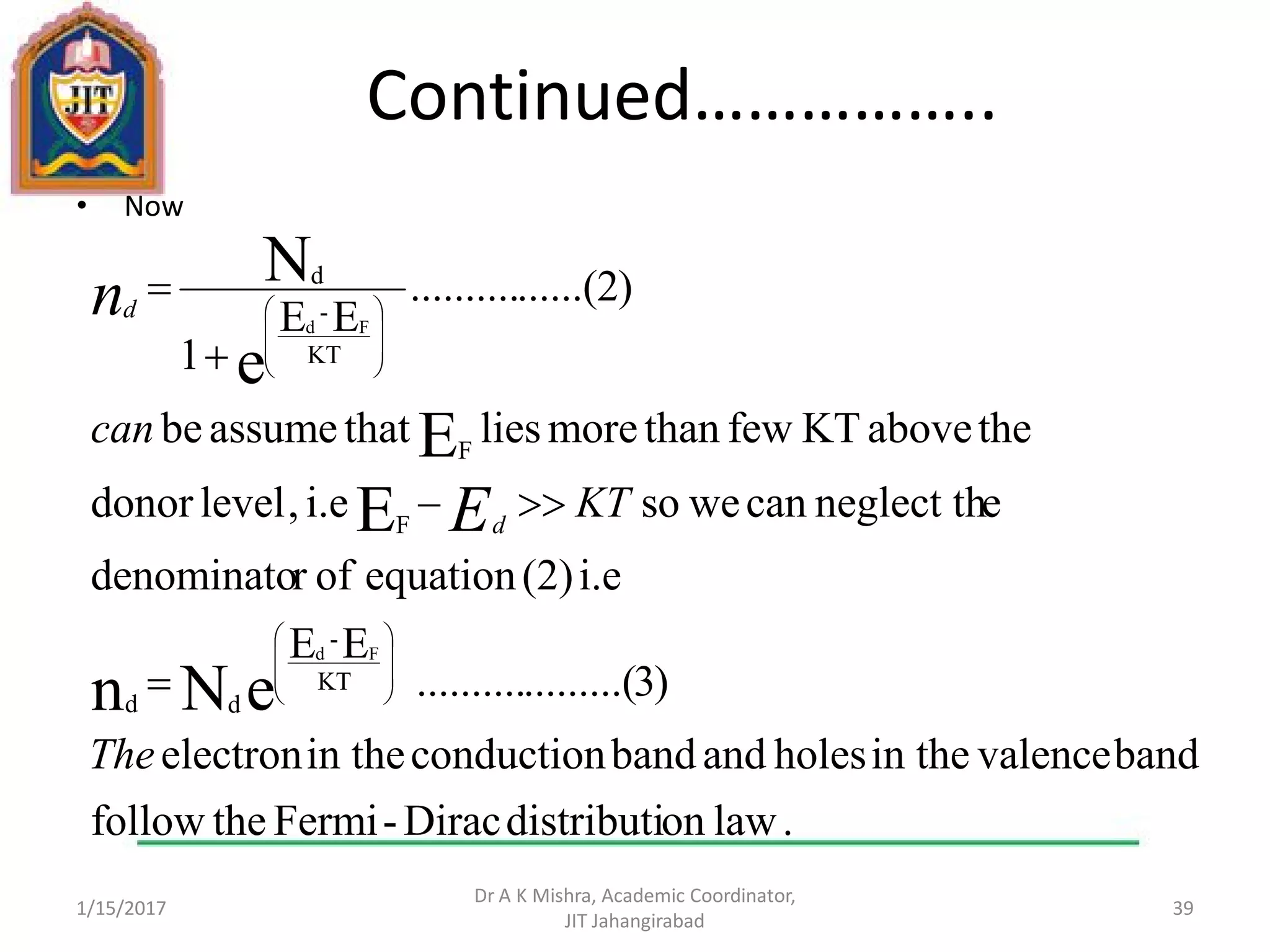

The document discusses key concepts of electronics and semiconductor theory, explaining the atomic structure of elements, electron properties, and the classification of materials as conductors, insulators, and semiconductors based on their electronic properties. It emphasizes the role of valence electrons in determining these properties and introduces the band theory of solids, which explains the energy levels and bands associated with electron conduction. Additionally, it explains the Fermi-Dirac distribution and energy gaps that influence electrical conductivity in different materials.