Downloaded 1,320 times
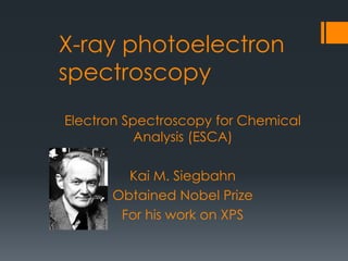
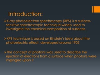
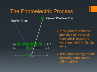
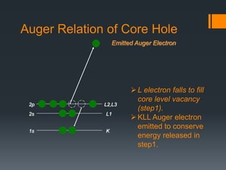
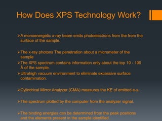


X-ray photoelectron spectroscopy (XPS) is a surface-sensitive technique that uses X-rays to eject electrons from a material's surface and measure their kinetic energy to determine the elemental composition and chemical states. Kai Siegbahn developed XPS in the 1950s and won the Nobel Prize for his work. A study used XPS to analyze the surface chemistry of langasite crystals before and after vacuum annealing, finding that higher-temperature annealing reduced the surface concentration of gallium. XPS provides quantitative and chemical state information from the top 10-100 Angstroms of a surface.


